Note : Les descriptions sont présentées dans la langue officielle dans laquelle elles ont été soumises.
-1- RCA 85,5 1 2
~ ~ 20487~9
MET~OD AND APPARATlJS FOR DEFEATING TT~F. OPERATION OF AN IC BUILT-
IN NOISE INVERTER
BA('K(~O~1ND
The present application concerns a television receiver having an
integrated circuit with a built-in noise inverter circuit and external circuitryfor defeating the operation of the noise inverter, e.g., in order to process a
scrambled television signal.
In subscription television systems premium or pay television
10 signals are tr:ln~mittPd "over the air", or via a cable network, or satellite in
some scrambled form. Such signals are descrambled for viewing by means of
a suitable decoder associated with the television receiver of an authorized
system subscriber. The decoder is usually situated in a converter unit located
external to the television receiver. The television signals may be grouped
15 into several levels, or tiers, each representing a different programming
category such as sporting events, movies, etc. The decoder of a particular
subscriber is authorized to descramble the television signals in selected
categories or channels, with the television signals in remaining unauthorized
categories or channels being coupled to the television receiver in scrambled
20 form.
A horizontal synchronization signal suppression technique is often
used to scramble the television signal. In such a "~u~u~ ,ss~d sync" technique,
scrambling is accomplished by suppressing the horizontal image
~yllc~llui~izillg (sync) pulse C;>lllpO~ltllt of the television signal. This causes the
2 5 horizontal deflection system of the receiver to lock onto random video signal
peaks during the active video line trace interval, rather than locking onto the
actual horizontal sync pulses during the retrace interval, thereby producing
an unstable and thereby unviewable displayed image.
Each system subscriber is provided with a decoder unit having a
3 0 "front end" circuit which includes conventional tuning, intermediate
frequency (IF) and video detection stages. Also, an 1~ n s~i~ gain control
circuit is provided within the decoder for controlling the gain of the tuning
and IF stages in accordance with the output of the video detection stage. A
sync restoration circuit operates during the suppressed sync pulse interval of
3 5 the video signal developed at the output of the video detector stage for
producing standard horizontal sync pulses. These sync pulses are
continuously inserted in the video signal developed at the output of the video
detector stage for producing a "descrambled" video signal suitable for viewing
on a standard television receiver. The descrambled video signal with
40 restored sync pulses is afterwards impressed on a standard television channel ~L
. .
-2- 2~487~9 RCA 85,512
RF carrier signal by means of an RF modulator, and then coupled as a
descrambled RF television signal to an antenna input of the television
receiver.
Each decoder may additionally include a decode authorization
5 circuit storing a unique subscriber code which is compared to a subscriber
authorization code transmitted during a horizontal line of the vertical
blanking interval of the television signal. If the stored subscriber code and
the transmitted subscriber authorization code compare favorably, a decode
authorization signal is developed for enabling the decoder, which is otherwise
1 0 disabled.
Decoder systems for descrambling a ~up~ ,ssed sync video signal
are discussed in U.S. Patent No. 4,408,225 of Ensinger, et al., for example.
Television receivers commonly include a video signal responsive
noise suppression circuit, such as a noise inverter, for suppressing noise
15 pulses which occur during sync pulse intervals of the video signal by means
of a signal inverting or equivalent technique. This action prevents noise
pulses from disrupting the operation of subsequent sync separator circuits,
and also prevents noise pulses from interfering with automatic gain control
(AGC) action of the receiver.
2 0 The presence of a video signal responsive noise suppression
circuit such as a noise inverter in a television receiver may adversely affect
the processing of a scrambled television signal such as a suppressed sync
signal. For example, in a ~u~ ssed sync type of scrambled signal, vertical
blanking interval signal components should not be suppressed when the
2 5 vertical blanking interval contains coded information, typically in digital
(binary) form, for use by the scrambled signal decoder. The coded
information may represent an authorization code for enabling the decoder to
operate, a code which identifies the type of scrambling used, or a code which
assists in the descrambling process in some other way.
3 0 In a video signal processing system which is subject to processing
a scrambled video signal and which includes a noise suppression net~ ork
such as a noise inverter responsive to video signals, it is desirable to includeapparatus for defeating or disabling the operation of the noise suppression
network during a descrambling operation to prevent distortion of coded
3 5 information occurring during prescribed intervals such as vertical bl;~nl~ing
intervals .
The size, cost and comple~.ity of a decoder are increased h~ the
need for the decoder to include an RF tuning stage, IF stage, video ~ tor
stage, AGC stage, and RF modulator, which stages ~except for the mo~ul.l~or)
40 duplicate stages already found in the "front end" of a television r.~ r
2~4~75~RCA 85,512
Thus it is desirable to provide a decoder which does not require such stages.
Accordingly, the Electronic Industry Association (EIA) of the United States has
proposed a decoder-receiver interface standard which simplifies the design of
decoders for use in ~u~ ,sscd sync television signal systems for elimin:l~in~
5 the need for the aforementioned tuning, IF, detector, AGC, and mod~ rf r
stages in a suppressed sync decoder unit. As outlined in EIA Consumer
Products Standard IS-15 "NTSC Television Receiver Audio/Video Baseband
Interface Specification," the EIA decoder standard provides a mutually
agreeable convention, to both television receiver manufacturers and the
10 subscription TV industry, for the implementation of a standardized sync
suppressed video decoder system.
One of the major impediments to implementation of the multiport
standard has been the difficulty of disabling or defeating the operation of the
noise inverter internally built into integrated circuits (ICs) commonly used in
15 processing video signals in television receivers. Heretofore, specially
designed integrated circuits had to be used which were designed for
permitting the noise inverter to be selectively disabled or defeated.
Approaches using such specially designed integrated circuits are described in
U.S. Patent No. 4,670,904 of the same inventor and is assigned to the
20 predecessor of interest of the present assignee. In the arrangement describedin the '904 patent, the operation of the noise inverter is selectively controlled
by a comparator on the integrated circuit having a terminal accessible
external to the IC for activation of the comparator in order to disable the
noise inverter when the decoder is operating. Additionally, the magnitude of
2 5 the AGC voltage is changed when the decoder is operative for activation of the
comparator. However, this arrangement employs an IC specifically designed
to provide for such selective disablement.
There are many video signal processing ICs which are
commonly available for utilization in television receivers which do not have
3 0 provisions for defeating the operation of the noise inverter and therefore do
not lend themselves for use with a decoder.
Accordingly, it is desirable to be able to defeat the operation of
the built-in noise inverter of a "standard" or "off-the-shelf" IC designed for
video signal processing so that a receiver/decoder according to the EIA
3 5 multiport standard can be implemented with such standard ICs.
SUMMARY QF THE INVENTION
Briefly. the present invention relates to apparatus for defeating a
particular signal processing circuit of a standard signal processing integrated
40 circuit which does not have an external access terminal or pin for defeating
~ 2 ~ ~ ~ 7 ~ ~
the signal processing circuit by modifying a feedback signal produced after
the signal processing circuit and available via an external accessible terminal.In the exemplary embodiment, the signal processing circuit is a noise inverter
and the IC does not include apparatus for controlling the noise inverter via an
S access terminal. However, the operation of the noise inverter is defeated by
modifying an automatic gain control (AGC) signal fedback to a gain control
stage via an AGC filter terminal. Specifically, the operation of the noise
inverter is defeated by changing the amplitude of the feedback AGC signal for
changing the gain of amplifier stages preceding the noise inverter so that the
10 signal fed to the noise inverter does not exceed a threshold level required for
operation of the noise inverter. This enables use of an EIA multiport
standard decoder with a standard IC in which the noise inverter is not
directly defeatable.
1~ BRIEF DESCRIPTION OF THE DRAWINGS:
FIGURE I shows a portion of a television receiver with apparatus
according to the present invention coupled to a decoder including ~up~ ,s~d
sync restoration apparatus;
FIGURE 2 is a block diagram representation showing the normal
20 operation of an exemplary noise suppression or inverter circuit commonly
employed within a standard integrated circuit;
Figure 3 is a block diagram representation showing apparatus
according to aspects of the present invention for defeating the operation of a
noise inverter incorporated in an IC;
2 5 Figure 4 is a schematic representation showing the internal
circuitry of portions of the apparatus of Figure 3, and
Figure 5 is a block diagram .t;~lese..l~tion showing an alternate
embodiment of a portion of the apparatus shown in Figure 3.
3 0 DETAn .F.n DESCRIPI~ON OF THF. PREFFI~RED EMRODIMENT
Referring now to FIGURE 1, a source 40 is a source of RF television
(TV) signals which can include suppressed sync scrambled RF TV signals such
as may be provided by a cable TV subscription service. In some systems the
television signal may contain digital information in reference portions of, e.g.,
3 5 vertical blanking intervals. The digital information represents coded data
which may be used by a scrambled signal decoder as previously discussed.
Briefly, the RF signals from source 40 are coupled to a television
receiver having, e.g., including a tuner 42, surface acoustic wave (SAW) filter
44, and other units as will be discussed more fully hereinafter, where the
4 0 television signal is demodulated to produce scrambled video and sound
,
` 2~7~9
- 5 - RCA 85,512
.
representative signals. A decoder unit 100, external to the receiver, restores
the sync component of the scrambled video signal, and the restored sync
(unscrambled) video signal is processed by the receiver in a conventional
fashion to produce an image on a CRT.
More specifically in FIGURE 1, tuner 42 receives the RF signals
from source 40 and in a mixer (not shown) translates the RF signal of a
selected TV channel to an intermediate frequency (IF) signal including video
and sound carriers at, e.g., in the United States, 45.75 MHz and 41.25 MHz,
respectively. The IF signal includes an amplitude modulated (AM) video
10 carrier of the vestigial sideband type representing the composite video
information, and a frequency modulated (FM) sound carrier containing the
sound information.
In the exemplary embodiment, the IF input signal received from
tuner 42 is coupled via a preamplifier (not shown) and an adjacent channel
15 sound trap (not shown) into two separate channels for sound and video
information demodulation according to quasi-parallel practices via the dual
channels of SAW filter 44. Additionally, in the exemplary embodiment, the
integrated circuit (IC) discussed is an integrated circuit No. TA8360
manufactured by the Toshiba company of Japan.
A first differential output 44a of the SAW filter 44 associated with
the video channel is coupled to signal input terminals 4 and 5 of an integrated
circuit network 45 via an in~ c~lnre-resistance circuit 46 which tunes out the
capacitance normally associated with the SAW filter output, and via an AC
coupling capacitor 47. The video channel portion of SAW filter 44 associated
2 5 with output 44a exhibits a response which matches the vestigial sideband
video component of the IF signal and which alt~ .altis the 41.25 MHz sound
carrier signal.
The quasi-parallel sound channel portion of SAW filter 44
associated with a sound output 44b is coupled to signal input terminals 8 and
3 0 9 of integrated circuit network 45 in the same manner as the video
component via an inductance-resistance circuit 48 and via an AC coupling
capacitor 49. The sound channel portion of SAW filter 44 at sound output
44b exhibits a double humped response with a first peak amplitude response
at the sound carrier frequency and a second peak amplitude response at the
3 5 video carrier frequency for providing a video carrier stripped of video
modulation to the sound demodulator for providing a relatively buzz free 4.5
sound intercarrier frequency signal after the first sound detector.
In the video IF channel, the video COlllpOL~ of the IF sign~l at
input terminals 4 and 5 of integrated circuit network 45 is coupled to ~n IF
40 amplifier stage 50 which includes a plurality of gain controllable IF ampli~iers
-6- 20~87~ RCA 85,512
(not shown). The amplified video component from stage 50 is AC coupled to a
limiter 52 and to a video detector 54 (e.g., a four quadrant multiplier). A
bandpass filter tank circuit 59 coupled via terminals 26 and 27 to the output
of limiter 52 is tuned to the video carrier frequency of 45.75 MHz. Limiter
5 52, filter 59, and video detector 54 form a quasi-synchronous video detector
for producing a baseband composite video signal at the output of detector 54.
The composite detected video signal is coupled via an amplifier 55 to a noise
inverter (NI) 56 which in this case normally alters black-going blanking
interval noise pulses below a given threshold level to prevent the noise
10 pulses from disrupting the operation of subsequent sync separator circuits
(not shown) and to prevent the noise pulses from interfering with automatic
gain control (AGC) action. The operation of noise inverter 56 will be
described in detail with reference to Figure 2.
Briefly, as will be discussed more fully hereinafter, the baseband
15 video signal output of noise inverter 56 is coupled via a terminal 25, to a
buffer amplifier 57, switch 58, and a video signal processor 60 including, e.g.,sync separator, luminance and chrominance frequency selection, and
Iuminance and chrominance processing circuits for developing R, G, and B
color image representative signals for forming an image on a CRT. A signal
20 derived from the output signal of noise inverter 56 is also coupled to an
external AGC detector 61 and from there to an internal AGC detector 62. In
the exemplary embodiment, internal AGC detector 62 detects the peak of the
horizontal sync component of the baseband video signal after noise inversion
(suppression) to develop an AGC control voltage related to the magnitude of
2 5 the sync component. The AGC voltage is normally directly coupled at
terminal 30 via an AGC filter network, capacitor 63. AGC amplifier 66 is
coupled to a gain control input of IF amplifier stage 50 for controlling the gain
of the amplifiers within stage 50 in accordance with the level of the AGC
detected sync pulse to maintain a desired nominal signal gain for the video IF
30 channel. The AGC output voltage from AGC amplifier 66 is also applied to an
RF AGC comparator amplifier 70, which provides an amplified AGC voltage to
a gain control input of tuner 42 via an RF AGC circuit 72. RF AGC circuit 72 is
of conventional design and includes a comparator responsive to a reference
voltage and to the AGC voltage derived from terminal 30 for providing an
3 5 output gain control signal which determines the gain status of tuner 42. A
potentiometer 74 coupled via a terminal 2 to a reference input of comparator
70 establishes the operating threshold of RF AGC comparator 70 to determine
the point at which comparator 70 conveys the AGC control voltage to circuit
72.
-7- 2~4~75~ RCA 85,512
An automatic fine tuning (AFT) detector 75, operatively associated
with a bandpass filter tank 76 tuned to the 45.75 MHz video carrier, responds
to the amplitude limited video IF carrier signal from limiter 52 for developing
an AFT voltage which is coupled via a buffer amplifier 77 and a terminal 29
5 to an AFT control input of tuner 42 to maintain proper tuning.
In the sound IF channel, the IF signals at terminals 8 and 9
including sound and video components is coupled to an IF amplifier stage 80
which includes plural gain controllable amplifiers. An amplified IF signal
from stage 80 is AC coupled to a limiter 82, to a video IF detector 84, and to a10 sound IF detector 86 via a capacitive phase shifting network 87. Detectors 84and 86 illustratively comprise four quadrant multipliers. A bandpass filter
tank 85 coupled via terminals 22 and 23 to the output of limiter 82 is tuned
to the video IF carrier. Limiter 82, detector 86 and tank 85 form a mixer for
providing a 4.5 MHz FM intercarrier sound signal from the sound and video
15 carrier components of the IF signal. The intercarrier sound signal from
detector 86 is coupled via an amplifier 88, a terminal 21, a buffer 89, a 4.5
MHz bandpass filter 90 and terminals 18 and 19 to a network comprising
cascaded, progressive limiting stages 91, 92 and 93 which provide an
amplitude limited FM intercarrier sound signal to an FM detector 95. Delector
20 95 operates together with a discriminator tank circuit 96 coupled to terminals
15 and 16 for generating a demodulated baseband audio signal. The audio
signal is applied to an audio signal processor stage (not shown) including
power output audio amplifiers and loudspeakers.
Automatic gain control of the sound IF channel is achieved in
25 response to a control voltage derived from the output of video IF detector 84.
The detected output signal of detector 84 is coupled via an amplifier 78, a low
pass AGC filter including a resistor 79 and a capacitor 81, coupled to a
terminal 10, and an AGC amplifier 83 to a gain control input of sound IF
amplifier stage 80.
3 0 The system of FIGURE 1 also includes a ~u~ s~d sync decoder
100 designed in accordance with the EIA multiport standard. The baseb~nd
composite video signal developed at terminal 25 of circuit 45 is applied to a
signal input of decoder 100 via buffer 57, which exhibits a suitable output
driving impedance as specified by the EIA standard, e.g., 75 ohm~. A
3 5 baseband video signal with a restored horizontal sync component is pro~ idedat the output of decoder 100. The output signal of decoder 100 is f~.~ to
external AGC detector 61 via input DRS (decoder restored sync) of s~it~h 58
when decoder 100 is in use.
Switch 58 can be a manual viewer controlled switch. ,Ir a
40 microprocessor controlled electronic switch responsive to both user ~ on
,
-8- 2~4~7~9 RCA 85,512
signals and automatic control signals received from the decoder, depending on
the characteristics of a particular decoder system. Switch 58 is placed in a
DRS position when decoder 100 is present and operative to decode a received
~u~ s~d sync television signal. Switch 58 is placed in a "NORM" (normal)
5 position when decoder 100 is either absent or inoperative in the presence of a received television signal with proper (non-~upp,~,ss~d) sync.
The operation of noise inverter 56 is defeated, as discussed more
fully hereinafter, when decoder 100 is operative to descramble a suppressed
sync video signal by restoring the sync component to the video signal. Thus
10 noise inverter 56 is prevented from distorting or destroying information suchas coded digital information which may be contained in the vertical blanking
interval of the scrambled television signal as discussed hereinabove. In this
regard the scrambled suppressed sync signal containing such digital
information, as applied to the input of decoder 100, may exhibit the form
15 indicated by the waveform illustrated adjacent to the input of decoder 100.
In the illustrated waveform, digital (binary) signal information is contained ina reference portion of a vertical blanking interval V, and suppressed
horizontal sync components are respectively included in horizontal blanking
interval portions of horizontal line intervals H.
2 0 The EIA multiport standard requires that the sync tip voltage of
the restored sync video signal developed by decoder 100 be substantially
equal to +1.0 volt under correct normal signal gain conditions. The more
positive the sync tip voltage is, the higher the signal gain is under AGC
control. Conversely, the less positive the sync tip voltage, the lower the signal
2 5 gain is under AGC control. Thus, the AGC circuits adjust the gain of the
receiver amplifiers to produce a correct video signal gain. The operation of
amplifier 57 and external AGC detector 61 are used to modify this "normal"
AGC operation to defeat the operation of noise inverter 56 which will now be
discussed.
3 0 The normal operation of a noise inverter 56 is shown in Figure 2,
wherein it is assumed an unscrambled video signal 128 is fed to input
terminal 130 of noise inverter 56. Signal 128 has negative going blanking
and sync pulses with a trace portion 132 having an exemplary 100 IRE
voltage level of +2.0 volts, a blanking porch level 134, and a sync level 136
3 5 having an exemplary voltage level of 1.0 volts. Video signal 128 contains
exemplary positive and negative noise pulses 138.
Noise inverter 56 has an exemplary threshold of +0.7 volts.
Signals less positive than the threshold level are clipped or clamped. Thus,
only noise pulses exceeding this threshold in the negative di}ection are
40 effected. The signal at 130 is fed to a comparator 140 and an electronic
- 9 - RCA 85,512
` 2048759
switch 142. Comparator 140 is provided with an exemplary reference of 0.7
volts and switch 142 is provided with a +1.3 clamp voltage. The output from
COIllp~la~Ol 140 is fed to switch 142 as a switch control signal. Switch 142
normally conducts the signal appearing at input terminal 130 to output
5 terminal 144. When a negative noise spike more negative than +0.7 volts
occurs, switch 142, responsive to an output from comparator 140, will
momentarily switch to the "noise" position and clamp the noise spike to + 1.3
volts. Thus, in a sense, noise spikes more negative than +0.7 volts are
inverted. This has the effect of ~u~ ssi~lg any negative going spikes more
10 negative than +0.7 volts which might otherwise appear in the signal
appearing at output terminal 144. The waveform of the signal at output
terminal 144 is shown at 146.
While there are no terminals provided for directly defeating the
operation of noise inverter 56, according to an aspect of the invention, the
15 operation of noise inverter 56 is defeated by reduction of the amplitude of
the video signal at 130 by action of the AGC circuitry modifying the feedback
by moving the sync tip 136 of signal 128 shown in Figure 2 above and away
from the noise inverter threshold voltage. Since the video amplitude is
reduced below the normal amplitude before application to noise inverter 56,
2 0 the amplitude of the video signal is restored to the desired level after the noise inverter external to IC 45 before application to decoder 100.
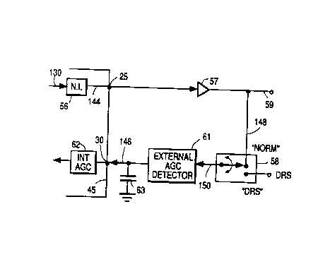
Circuitry for defeating the operation of noise inverter 56 is shown
in the block diagram of Figure 3. Internal AGC detector 62 of integrated
circuit 45 is designed so that a desired, correct signal level will be produced
25 at signal output 144 of noise inverter 56 for a predetermined level of AGC
feedback voltage developed across AGC filter capacitor 63 normally coupled
to terminal pin 30. If the AGC feedback voltage developed at input pin 146 is
lower than the predetermined amount, the amplification within IC 45 is
decreased. As a result, the signal level at the input of noise inverter 56 is
30 decreased with a corresponding decrease at output terminal 144. In accord
with aspects of the present invention, the AGC feedback voltage at terminal
pin 30 is intentionally modified to, in a manner of speaking, "trick" or "fool"
the circuit into thinking that the signal level at 144 and amplification
subsequent thereto is higher than nominal. This causes the amplification
3 5 provided by the IC network 45 prior to noise inverter 56 to be lowered.
Thus, in turn, reduces the signal level at input 130 of noise inverter 56 by 2-
3 db. As a result, the lowest portion of the sync tips is caused to be less
negative than the threshold required for operation of noise inverter 56, thus
defeating the operation of noise inverter 56. The AGC feedback signal at 146
-lo- ~87~9 RCA 85,512
is modified by external AGC detector 61 which is coupled to internal AGC
detector 62 of IC 45 via pin 30.
Since the output from noise inverter 56 at 144 is caused to be 2-
3 db low, amplifier 57 is provided to make up for this loss so that the signal
5 available at amplifier output 59 and switch input 148 is at the nominal level.Thus, the signal at 148 is a proper level video signal (i.e., as if the signal level
at noise inverter 130 had not been modified) and can be fed to decoder 100
as a multiport video signal meeting the EIA multiport standard. In the
exemplary embodiment, amplifier 57 also adjusts the DC offset of the signal at
10 148 so that the most positive peaks of the trace signal at 148 is at 100 IRE
(maximum brightness).
The signal at 148 is fed to switch 58 which is provided for
choosing the input source for input 150 of external AGC detector 61. In the
exemplary embodiment, the "norm" position selects the signal at 148 for
15 input to external AGC detector 61. When a decoder 100 is used and switch 58
is in the DRS (decoder restored sync) position, the decoder restored sync (DRS)
output signal of decoder 100 is fed to input 150 of external AGC detector 61.
As a result, decoder 100 is part of the feedback loop which the AGC circuit
controls. It is noted that the signal at 148 is a "correct" signal level with the
20 arrangement shown in Figure 3, noise inverter 56 is permanently disabled
whether or not decoder 100 is utilized, and therefore external AGC detector
61 causes the signal fed to noise inverter 56 to have a reduced level signal.
An alternative embodiment for selectively defeating the operation of noise
inverter 56 with external AGC detector 61 still in the circuit will be discussed2 5 hereinafter in connection with Figure 5.
Figure 4 is a schematic showing the circuit details for amplifier 57
and external AGC detector 61. Buffer amplifier 57 accomplishes two things.
Firstly, it amplifies the signal an additional 2-3 db to co~ ,c.lsate for the loss
of gain of 2-3 db instituted prior to the input of noise inverter 56 in order to30 defeat the operation of noise inverter 56. Secondly, it adjusts the DC level of
the signal so that the m~ximllm level of the trace portion is at 100 IRE
(maximum white).
Noise inverter output signal at 144 is fed to a filter 152 which is a
4.5 Mhz sound intercarrier trap, and in turn to a PNP transistor 154 having a
3 5 base electrode coupled to an exemplary power supply of five volts (not
shown) through resistor 156, a collector electrode coupled to ground through
a load resistor 158, and an emitter electrode coupled through a resistor 160
to a variable voltage source comprising a potentiometer 162 coupled between
a power supply and ground. Transistor 154 provides the desired additional
40 amplification, with potentiometer 162 being adjusted to provide the desired
=
:
-11- RCA 85,5 1 2
2048759
DC level. The shift in the DC level CO~ c~r.s for the shift caused by the
AGC m.o.1ifi~ tion. The signal across load resistor 158 is coupled to a base
electrode of an emitter follower NPN transistor 162 having an emitter
electrode coupled to ground through divider resistors 164 and 166, and a
5 collector electrode coupled to the power supply.
The video output terminal 59 shown in Figure 3 is symbolic. In
the exemplary embodiment shown in Figure 4, for an internal video signal
processed in the nominal manner by the remainder of the television receiver
for processing by decoder 100, a video signal output is developed at a
10 terminal 168 coupled at only the emitter electrode, an EIA multiport standardvideo signal is developed at terminal 170 coupled thereto through resistors
172 and 174. Feedback resistors 176 and 178 are coupled from the emitter
electrode and the junction of resistors 172 and 174 respectively to the base
electrode of transistor 154. The output impedance at terminal 170 is 75
15 ohms as dictated by the multiport standard.
The output signal at 148 derived from the junction of resistors
164 and 166 is fed to the "norm" terminal of switch 58. As stated
hereinabove, the position of switch 58 determines which sync tip input signal
will be provided to external AGC external detector 61 at input terminal 150.
20 When no decoder 100 is turned on or provided, the switch 58 would be in the
"normal" position to feed the output signal from transistor 162 to input
terminal 150 of external detector 61. When a decoder 100 is operational in
the circuit, switch 58 would be in the "DRS" position and feeds the decoder
sync restored output signal to external AGC detector 61 so that the AGC circuit
2 5 senses the restored sync tip level. Resistor 188 coupled between the DRS
terminal and power supply is provided to comply with the EIA standard to
pull up the DRS terminal to power supply voltage when decoder 100 is not
connected and to provide a specified load impedance to the output of decoder
100.
3 0 The signal at 150 is coupled through an isolation resistor 180 to a
base electrode of PNP transistor 182 having a grounded collector electrode,
and an emitter electrode coupled to a low pass filter capacitor 184 and a
resistor 186 coupled to the power supply. This arrangement functions as a
negative peak detector. Transistor 182 conducts more highly as its base
35 electrode becomes more negative. Thus, the larger the peak negative signal
at the base electrode is, the more transistor 182 will conduct, and the lower
will be the voltage across capacitor 184.
A PNP transistor 190 amplifies the voltage developed ~cross
capacitor 184. A base electrode of transistor 190 is coupled to receive the
40 detected AGC voltage developed across capacitor 184 and has an emitter
- 1 2- RCA ~5,512
20487~9
elect}ode coupled through a resistor 193 to a bias providing variable voltage
potentiometer 194 coupled between the power supply and ground. The bias
provided by potentiometer 194 is set for adjusting the DC offset of the AGC
signal to compensate for variations of the DC level of the video AGC
S characteristics of the signal. A collector electrode of transistor 190 is coupled
to ground through a resistor 196 and to a base electrode of a transistor 192.
Transistor 192 has an emitter electrode coupled to ground through resistor
198 and a collector electrode coupled to AGC input line 146 of integrated
circuit 45. Transistor 192 provides a voltage to current conversion for
10 providing a current source drive to AGC capacitor 63 coupled between line
146 and ground.
As noted earlier, the above discussed circuits provide a system
wherein the integrated circuit built-in noise inverter 56 is permanently
defeated. An alternate embodiment, wherein noise inverter 56 can be
15 selectively defeated, is shown in Figure 5. Figure S is similar to the block
diagram of Figure 3 except that a switch 200 has been added between
amplifier 57 and terminal 170 and divider resistors 202 and 204 have been
added in parallel with the output of amplifier 57 and coupled between
terminal 170 and the power supply.
2 0 Resistors 202 and 204 are attenuator resistors for providing at
206 an output signal from amplifier 57 which is 2 db less than the output
signal otherwise available. Switch 200 has a "norm" and "DRS" position which
can be ganged to the similarly labeled positions of switch 58. In the "DRS"
position, when defeat of the operation of noise inverter 56 is desired, the
2 5 operation is the same as with Figure 3. In the normal position, when the
operation of the noise inverter 56 is is desired, the signal at terminal 170 is
reduced by 2 db. This causes the AGC detected by AGC detector 61 to be
lowered which in turn causes the gain of the IF amplifiers intern~l to
integrated circuit 45 to increase. This increase in gain brings the signal
30 strength at 130 up to its normal operating level and the noise inverter 56
becomes operational.
The disclosed arrangement can also be used in conjunction with
other television receivers such as a video cassette recorder (VCR ) . In
addition, while the exemplary embodiment has been discussed with ref~rence
3 5 to an integrated circuit (IC) or chip, the invention may be used as well with
sealed or potted modules and the like in which the internal circuitr~ is not
available subsequent to the manufacture thereof for external el~ctrical
connection thereto or manipulation thereof except through t~r~ n~ls
provided for such a purpose in a casing, housing, or enclosure.