Note : Les descriptions sont présentées dans la langue officielle dans laquelle elles ont été soumises.
- I 20~929~
Power Amplifier
This invention relates to power amplifiers, such as pulsed
power amplifiers, for amplifying radio frequency signals. This
5 invention particularly relates to power amplifiers for use in GSM
radio transmitters.
A pulsed power amplifier which may be used in GSM mobile
radio tr~ncmitters is described in ~n~ n patent application No. 613,572
filed on September 27, 1989.
This application discloses a burst modulated power
amplifier whose output power characteristics upon turn-on and
turn-off are controlled by power control signals which are
dependent on a sequence of values stored in a memo~ of a power
control section of the power amplifier. The power amplifier can
operate at a number of different output power levels and a
sequence of values is stored in the memory for each of these
power levels. Once a power level has been selected, the
corresponding sequence of values is selected and read from the
memory .
2 0 The output power of a GSM mobile radio transmitter must
be adjustable between sixteen power levels. In order to account
for tolerance factors within the amplifier which will affect the
ultimate output power, there are generally sixteen nominal power
levels which are each spIit into four sub-levels close to the
2 5 nominal value. A transmit controller of the power control section
can then determine which of the sixty-four sub-levels is best to
represent each one of the sixteen nominal power levels. There are
therefore sixty-four sequences of values stored in the memory
corresponding to the sixty-four power levels.
3 0 Each of the sequences of values represents a ramp-up
waveform and a ramp-down waveform corresponding to turn-on
and turn-off respectively. One ramp-up waveform can be
satisfactorily represented by a sequence of 64 bytes (512 bits) to
be stored in the memory and one ramp-down waveform can be
3 5 satisfactorily represented by a sequence of 64 bytes to be stored
in the memory. Thus, the total number of bytes of memory
required to store the sixty-four sequences of values is 8192 bytes
Y~ ~
WO 91/12661 r~ 2 pcr/Ep9l/ool46
~ 2~9~99 ~
(65536 bits). This is significantly large particularly when the
power control section is integrated in an integrated circuit.
It is therefore desirable to reduce the number of bytes of
memory required to store all the sequences of values for the
5 different power levels.
In accordance with a first aspect of the invention there is
provided a power amplifier being responsive to a power level
control signal for amplifying radio frequency signals to define any
one of a plurality of amplifier output power envelopes, the power
l 0 amplifier comprising:
means for generating a predetermined time varying signal
which represents a predetermined one of said plurality of
amplifier output power envelopes;
means for modifying said time varying signal in response to
l 5 said power level control signal for definition of a selected output
power envelope; and
control means for controlling the amplifier output power in
response to said modified time varying signal to amplify the radio
frequency signal according to the selected one of said plurality of
2 0 output power envelopes.
In a preferred embodiment, the modifying means comprises
means for clipping the time varying signal at a value which
depends on the power level control signal.
In a second embodiment of the invention the modifying
2 5 means comprises means for multiplying the time varying signal
by a scaling factor which depends on the power level control
signal.
In a third embodiment of the invention the modifying
means comprises combining means for combining a value with the
3 0 tirne varying signal. The value depends on the power level
control signal and may be a negative number or a positive
number bigger than or equal to zero.
The time varying signal may comprise a sequence of values
stored in memory which represents a predetermined one of the
3 5 plurality of amplifier output power envelopes.
The pulsed power amplifier may further comprise a filter
such as a low pass filter in order to smooth waveforms generated
by the modified sequence of values.
W O 91/12661 3 2 ~ 4 9 2 9 g PC~r/EP91/00146
Thus, it will be appreciated that by generating one sequence
of values representing one ramp-up and one ramp-down
waveform for all the different power levels and using the
modification means to modify the values in response to a
5 particular power level, a ramp-up waveform and ramp-down
waveform represented by a modified sequence of values can be
obtained for any of the power levels and since only one sequence
of values need be generated the total number of values is
considerably reduced. For the prior art power amplifier described
10 above, for example, only 1 28 bytes will be required instead of
8 192 bytes.
Three pulsed power amplifiers for amplifying radio
frequency signals will now be described, by way of example, only
with reference to the accompanying drawings in which:
Figure 1 is a block schematic diagram of a first pulsed power
amplifier in accordance with the present invention;
Figure 2 is a block schematic diagram of a second pulsed
power amplifier in accordance with the present invention;
Figure 3 is a block schematic diagram of a third pulsed
2 0 power amplifier in accordance with the present invention;
Figure 4 shows a diagr~mm~tic representation of a typical
output power versus time response of the pulsed power amplifier
shown in Figure 1 during turn-on; and
Figure 5 shows a diagr~mm~tic representation of a typical
2 5 output power versus time response of the pulsed power amplifier
shown in Figure 1 during turn-off.
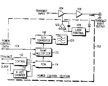
Referring to Figure 1, a power control section 2 is shown
coupled to an attenuator 4 which is controlled by a feedback loop
8. An RF signal is supplied to an input of the attenuator 4 whose
3 0 output is coupled to a RF power amplifier 6. The output of the
power amplifier is fed to an antenna (not shown).
The power control section 2 has a clock input CLK coupled to
a six-bit counter 10 which is coupled to the address lines of a ROM
14. A control 12, also coupled to the counter 10 and the ROM 14,
3 5 is controlled by the signal on the clock input CLK and a signal on
the transmit input TX. The control 12 is coupled to a ramp clipper
16 and to a digital-to-analog converter 18. ROM 14 provides an
eight bit output which is fed to the ramp clipper 16. The ramp
wo gl/12661 2 ~ 4 ~ 2 ~ 9.~ PCI`/EP91/00146
clipper 16 is controlled by power control data on a power control
data line 24 and its output is fed to the digital-to-analog converter
18, from which the resulting analog signal is fed via a low pass
smoothing filter 20 to a comparator amplifier 22 which is coupled
to the attenuator 4.
A sequence of values representing one ramp-up and one
ramp-down waveform is stored in the ROM 14. Since in the
preferred embodiment sixty-four bytes are required to represent
a ramp-up waveform, such as the ramp-up waveform A in Figure
4, and sixty-four are required to represent a ramp-down
waveform, such as the ramp-down waveform C in Figure 5, the
total number of bytes required is 128 bytes. The sequence of
values is addressed according to the signal on the address lines
coupled to the counter 10.
The operation of the power amplifier in accordance with the
invention will now be described. However, since the operation of
a power amplifier has been described in detail in the above
referenced patent application the operation will not be described
in detail.
At the start of transmission of a RF signal, a transmit
controller (not shown) selects a power level and sends a
corresponding signal on the power control data line 24 to the
ramp clipper 16. In addition, the transmit controller (not shown)
provides a transmit control signal indicating the start of
2 5 transmission to the transmit input TX and provides the RF data to
be fed to the input of the attenuator 4. On receipt of a 'start'
signal at the transmit input TX, under the control of the counter
10 and control 12, the sequence of values representing a ramp-up
waveform is read from the ROM 14 and fed to the ramp clipper
3 0 16. At the end of the transmission, the transmit controller (not
shown) provides an 'end' signal to the transmit input TX whereby,
under the control of the counter 10 and control 12, the sequence
of values representing the ramp-down waveform C is read from
the ROM 14 and fed to the ramp clipper 16.
3 5 The power control data signal sent on the power control data
line 24 controls the clipping level of the ramp clipper 16. .That is,
it determines the value in the sequence of values representing a
ramp-up waveform to which all the following values in the
Wo 91/12661 5 2 ~ 4 9 2 9 9 PCT/EP91/00146
sequence are clipped. The ramp clipperl6 adds the power control
data to the value from the ROM 14 and when this sum exceeds a
predetermined threshold, clocking of the digital-to-analog
converter 18 is stopped and the last clocked value is continuously
5 output from the digital-to-analog converter. For example, the
ramp-up waveform A is clipped above the point X if the power
level represented by waveform B is selected. For a ramp-down
waveform the signal determines the value in the sequence of
values to which all the preceding values in the sequence àre
l 0 clipped. Thus, the ramp clipper 16 in response to the signal on
the power control data line 24 clips the sequence of values at a
value that depends on the power control data signal in order to
obtain ramp-up and ramp-down waveforms which correspond to
the selected power level. The output of the ramp clipper is then
l 5 fed to the analog-to-digital converter 18 to be smoothed by a low
pass filter 20. The output power of the power amplifier is thus
controlled by the output from the low pass filter which is supplied
to the comparator amplifier 22 and the attenuator 4.
The signal on the power control data line 24 is constant
2 0 during a burst, i.e. during turn-on of the burst modulated power
amplifier, and can be changed between bursts so that a different
power level is selected for the next burst. It is necessary to have
a smoothing low pass filter since the clipping method will produce
sharp edges on the ramp-up and ramp-down waveforms. This
2 5 reduces the spectral noise generated by the power ramping.
The ramp clipper 16 may be replaced by a ramp multiplier
130 as in Figure 2 which shows a second pulsed power amplifier
incorporating the invention. Like components to those in Figure l
are referenced with the same reference numeral plus a hundred.
3 0 The operation of the second pulsed power amplifier is similar to
that of the first described with reference to Figures l, 4 and 5
except that the ramp-up and ramp-down waveforms for the
different power levels are obtained by multiplying the ramp-up
and ramp-down waveforms stored in the ROM l 14 with a scaling
3 5 factor. The scaling factor is determined by the signal on the
power control data line l 24.
Alternativelv, the ramp clipper 16 of the first pulsed power
amplifier may be replaced by a ramp adder or subtractor 232 as
wo 91/12661 ~ Q ~ 9 2 ~ 9 PCI/EP91/00146
in ~igure 3 which shows a third pulsed power amplifier
incorporating the invention. Like components to those of Figure 1
are referenced with the same reference numeral plus two
hundred. The operation of the third pulsed power amplifier is
5 similar to that of ~he first described with reference to Figures 1, 4
and S except that the ramp-up and ramp-down waveforms for the
different power levels are obtained by subtracting a value from
the ramp-up and ramp-down waveforms stored in the ROM 214.
The value to be subtracted is determined by the signal on the
10 power control data line 224.
It will be appreciated that although it is necessary that a
smoothing low pass filter be used with a ramp clipper due to the
production of sharp edges on the waveforms, such a low pass
filter is not necessarily required for the ramp multiplier and ramp
1 5 subtractor.
It will also be appreciated that although the preferred
embodiments of the invention have been described wherein a
sequence of sixty-four values are used to represent one ramp-up
waveform and another sequence of sixty-four values are used to
2 0 represent one ramp-down waveform and each value comprises
eight bits, these numbers are arbitrary and may vary with use of
the pulsed power amplifier. In addition, the number of desired
power levels may vary with use of the pulsed power amplifier.
In addition, although in the preferred embodiments
2 S described herein a ROM is used to generate a predetermined time
varying signal by storing a sequence of values, the time varying
signal may also be generated by analog means.
It will also be appreciated that the time varying signal may
also be a single step.