Note : Les descriptions sont présentées dans la langue officielle dans laquelle elles ont été soumises.
2~~~9~~~
FIELD OF THE INVENTION
The present invention pertains generally to
3 superconductor wires. More specifically, the present
~a invention pertains to apparatus for aligning several
superconductor filaments in a layer of superconductor
fi material. The present invention is particularly, but not
exclusively, useful in the manufacturing of a bendable cable
which is made of high temperature superconductor ceramic
g materials.
I1 BACKGROUND OF THE INVENTION
12 With the advent of superconductor materials which have
t3 superconducting transition temperatures (T~) above about
Kelvin, there has arisen the possibility of highly efficient
I~ transmission of electrical power, i.e., transmission
of
16 electrical power with substantially no transmission losses.
I; This potential, however, is very much dependent on the
ability
Ig to provide a structure which will support and protect
Ig relatively long transmission cables which are typically
made
of a bundle of individually manufactured high-T~
M
21 superconductor filaments.
RIo
Unfortunatel y g
,~OVN22 y, presentl known hi h-T
>m=m superconductor
m ~
xu,diL23
materials are ceramics which are relatively brittle and
0
fragile. Furthermore, they are particularly susceptible
to
r 25 breakage when subjected to tensile stresses, as compared
to
26 compressive stresses. Consequently, the structural
-1-
~~t~~ )~3~
limitations of ceramic superconductor materials are most
2 apparent when any bending (and, hence, potential tensioning)
I
3 of the superconductor may be necessary, as is commonly
4 required in a wide variety of potential applications.
To avoid imposing undue tensile stress on the ceramic
6 filaments of a superconductor cable when the cable is
bent, it
7 is desirable to support the cable in a structure which
has a
g larger cross-sectional area than the cable. More
y specifically, it is well-known that when a structure
is bent,
portions of the structure will be in tension and other
11 portions of the structure will be in compression.
12 Accordingly, when a structure which has a larger cross-
1;3 sectional area than the ceramic superconductor cable
is used
14 to support the cable, the superconductor cable can effectively
1; be positioned in that portion of the bendable support
structure which will be subjected only to compressive
17 stresses. As stated above, modern ceramic superconductors
can
lg withstand compression more readily than they can withstand
19 tension. Accordingly, it is necessary to form the cable
into
2o a relatively flat layer of coparallel superconductor
"-' 2t filaments, so that the cable will fit into the desired
N portion
m
~r
~
m
d aNm
w ~og~~22 of the supporting structure. furthermore, in the case
of
>mymm
~ i
~
,p
c~ 23 relatively long lengths of cable, it is desirable that
~, the
o
z
Q
000
W,: 2~ individual superconductor ffilaments which make up the
cable be
,=
A 25 automatically aligned and positioned in the supporting
26 structure.
-2-
CA 02049558 1998-09-04
SUMMARY OF THE INVENTION
2 In light of the above, the present invention provides an
.3 apparatus for manufacturing a cable from ceramic
superconductor filaments in which the filaments are aligned
into a coparallel, juxtaposed relationship ~~aith other
6 filaments in the cable. The present invention also provides
an apparatus for manufacturing a cable from ceram=~c
superconductor filaments which automatically aligns the
superconductor filaments in a layer of superconductor
material. The present invention also provides an apparatus
11
for manufacturing a cable from ceramic superconductor
12
filaments whicr is relatively easy to use and comparatively
13
cost effective.
14
1~ A device for aligning several (e. g., six or twelve)
16 superconductor filaments in juxtaposition to form a layer of
1; superconductor material includes a backboard and a number of
lg motor-driven supply spools. Each of the supply spools is
19 rotatably mounted on the backboard, and each of the supply
20- spools
holds
one end
of an
individual
superconductor
filament.
The respective
opposite
ends
of the
filaments
(i.e.,
the ends
21-
a ,~
'oo~N of the filaments which are not held an associated supply
on
, 22
>m~mm
'~
~ spool) are collectively attached to single rotatable wire
a
23
0
' S
~=W
take-up spool. Accordingly, the wire take-up spool can
be
w
24
rotated to transfer the filaments from the respective supply
25
2f~ spools to the take-up spool.
-3-
~~~~~8
The device of the present invention also includes a
2 combiner board. The combiner board is mounted on the
;3 backboard normal to the backboard between the supply
spools
4 and the wire take-up spool. One surface of the combiner
board
is formed with a guide channel which is tapered inwardly
(, toward the supply spools, i.e., the channel is incrementally
enlarged away from the supply spools to the take-up spool.
A
g series of curved, elongated grooves is also formed on
the
y combiner board, and each groove extends from the guide
channel
,p toward the backboard. More particularly, the grooves
of the
11 combiner board are sequentially aligned on the surface
of the
12 combiner board for individually receiving one of the
13 superconductor filaments and feeding the respective
14 superconductor filament into the guide channel. Stated
1~ differently, the combiner board individually receives
each of
1G the superconductor. filaments as the filaments are transferred
1; from the respective supply spools to the take-up spool.
As
lg the combiner board receives the filaments, the combiner
board
19 guides the filaments into alignment, i.e., the combiner
board
~
~
2o guides the filaments into a planar array wherein the
. filaments
x
2t are coparallel.
0
'~ _
a
:
n
'
w so'"22 Additionally, each supply spool has a tension controller
=
O
N
_
N
~
j
N ~p 23 individually associated with the respective supply spool.
~ ~,~=a In
W 5
00
24 accordance with the present invention, each of the tension
A 25 controllers engages the superconductor filament that
is
26 associated with the respective supply spool and establishes
a
-4 -
predetermined tension in the filament as the filament is being
transferred from the filament's associated supply spool
to the
3 take-up spool.
More particularly, each tension controller includes
a
pivot arm that is configured as a pendulum and has a
pivot end
6 rotatably attached to the backboard. Each pivot arm
also has
7 a free end that is fixedly attached to a hollow curved
guide.
8 The respective filament from the associated supply spool
is
g positioned through the lumen of the curved guide of
the
respective pivot arm and can consequently cause the
arm to
11 pivot when the take-up spool moves faster or slower
than the
1z feed spool. Mounted on the backboard adjacent each pivot
arm
13 is a respective optical position sensor which senses
the
position of the respective pivot arm when the associated
filament is under tension. Each respective position
sensor
16 generates a signal in response to the position of the
associated pivot arm. Also, a potentiometer is individually
~g coupled to the pivot end of each pivot arm to sense
the
Ig direction of pivotal motion of the arm and generate
a signal
in response. The signals from the respective potentiometers
M
,u O and optical sensors are sent to a respective signal
processor,
ki
mNm
a '~~'
w ;oN 22 which is electrically coupled to the motor of the respective
>rnemm
~
~
5: 23 associated supply spool. Each signal processor controls
~NO=s the
Woo
speed of rotation of its associated supply spool based
on the
A 25 signals from the associated optical sensor and potentiometer.
The respective signal processors thus match the speed
of the
-5-
~~) ~~ ~~~~
feed spool with the speed of the take-up spool and holds the
2 pendulum at a desired angle, of which this predetermined
angle
3 controls the tension on the filaments.
Additionally, each tension controller also includes a
second position sensor for sensing the position of the
6 associated pivot arm when the wire is substantially slack
or
7 broken. Each of the second position sensors accordingly
8 generates a signal. which is sent to the respective signal
9 processor which is electrically coupled to the respective
supply spool motor to stop the respective supply spool
motor
11 when the respective filament becomes slack or breaks.
Also,
12 the signal from each second position sensor can be coupled
to
13 an alarm for providing audio or visual indication of
when a
1a respective filament becomes slack.
The novel features of this invention, as well as the
16 invention itself, both as to its structure and its operation,
t7 will be best understood from the accompanying drawings,
taken
1g in conjunction with the accompanying description, in
which
1g similar reference characters refer to similar parts,
and in
r ..
,
2p which:
x
; o
2 T
x ~
~~
m
d a
!
~~
~
w ~~ga~~~,22 BRIEF DESCRIPTION OF THE DRAWINGS
>m~m
dS
s~~~
x ooZa2;; Figure 1 is a perspective view of the novel device for
W 5
W~
24 aligning superconductor wires of the present invention;
A
?~ 25
26
-6-
Figure 2 is a top view of the combiner board of the novel
device for aligning superconductor wires of the present
:; invention;
Figure 3 is a cross-sectional view of the combiner board
of the novel device for aligning superconductor wires of the
6 present invention, as seen along the line 3-3 in Figure 2 with
7 portions broken away for clarity;
H Figure 4 is a cross-sectional view of the combiner board
9 of the novel device for aligning superconductor wires of the
l0 present invention, as seen along the line 4-4 in Figure 2 with
11 portions broken away for clarity;
12 Figure 5 is a schematic diagram of one tension controller
13 of the novel device for aligning superconductor wires of the
14 present invention with portions shown in phantom for clarity;
and
1~, Figure 6 is a schematic diagram of the electrical
components of one tension controller of the novel for
device
lg aligning superconductor wires of the present invention.
19
,
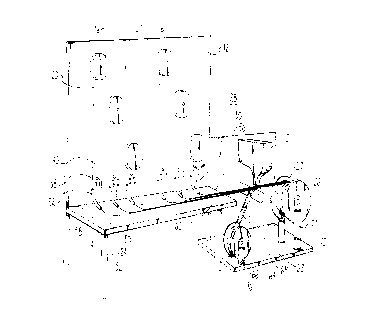
2p~ DESCRIPTION OF THE PREFERRED EMBODIMENT
a 2t Referring initially to Figure 1, a device for aligning
"
u
,m
m
a
<'~m
xSoo~N22 superconductor wires is shown, generally designated 10.
>m~mm
~:~'~~
Device 10 includes a backboard 12 and a combiner boardAs
14.
3
boo
24 shown, combiner board 14 is attached to or mounted on
A 25 backboard 12 substantially orthogonally to backboard A
12.
F
26 plurality of supply spools 16 are also shown mounted on
CA 02049558 1998-09-04
backboard 12. It is to be understood that supply spools 16
2 are rotatably mounted on backboard 12, and that each spool
16
3 can be rotated by a respective motor (one supply spool motor
4 18 shown schematically in Figure 5). It is to be further
understood that while Figure 1 shows six ( 6 ) supply spools
16,
6 device 10 can include a greater or lesser number of supply
r spools 16. For example, twelve (12) supply spools 16 can be
g mounted on backboard 12, if desired.
g As shown in Figure 1, each supply spool 16 is attached to
a respective superconductor filament 20. Each superconductor
11 filament 20 can be made of any suitable superconductor
12 material which has a superconducting transition temperature
13 above about twenty (20) Kelvin. In the preferred embodiment,
I4 each superconductor filament 20 is made of a superconductor
~3 material which has the chemical formula REBa2Cu30~_X, where
RE
16 is selected from the group consisting of yttrium and elements
1; having an atomic number between fifty seven (57) and seventy
lg one (71), inclusive, and x is from zero (0) to one half (.5),
19 inclusive. If desired, each filament 20 can have a nickel-
20. based support substrate and a silver-based protective
4
2I overcoating. Such a superconductor filament 20 is fully
C ,~
~ O
~
..vr
~ OINm
C U
~
N
N 22 disclosed in co-pending Canadian patent application
= m
m
a =
V
oV 23 2,049,554, filed August 20, 1991, entit~_ed "Process and
sa;
~~ 24 Apparatus fcr Fabrication of Silver-Coated High Temperature
..
25 Ceramic Superconductor Fiber on Metal Substrate", assigned
26 4 to the same assignee as the present inventicn.
_g_
~~~~~'~8
Still referring to Figure 1, each superconductor filament
20 is shown extending through a respective curved hollow
guide
a tube 22. Each guide tube 22 is curved outwardly from
backboard 12, i.e., each guide tube 22 is curved from
backboard 12 toward edge 24 of combiner board 14. Also,
each
6 guide tube 22 is curved from backboard 12 toward a rotatable
7 motor-driven take-up spool 26, which is attached to each
of
8 the filaments 20. Take-up spool 26 is operatively associated
9 with a drive motor 27. The guide tubes 22 receive the
respective filaments 20 through the respective lumens
of the
~1 guide tubes 22. The respective lumens of the guide tubes
22
12 can be coated with Teflon~.
13 Additionally, as shown in Figure 1, the guide tubes 22
14 are fixedly attached to respective tension controllers,
generally designated 28. More particularly, referring
briefly
16 to Figure 5, one tension controller 28 is shown to include
a
1 pivot arm 30 which is rotationally attached to backboard
r 12 at
lg a pivot end 32. Pivot arm 30 is a pendulum which is fixedly
lg attached to guide tube 22, so that as guide tube 22 moves
in
response to differences in speed between the take-up
and feed
M
spool, pivot arm 30 also moves. Stated differently, the
tG
~
V
w ENO<"~22 tension of filament 20 depends on the angular position
~,
>m_m~,
W oN 2,~ relative to the free-hanging position) of pivot arm 30.
o Pivot
Z
~
W 5
W~8
end 32 of pivot arm 3o is mechanically coupled to the
center
w~
A 25 tap 34 of a potentiometer 36 (shown schematically in
Figure
2~ 6) Thus, as pivot arm 30 pivots, the resistive setting
of
_g_
~Q~~~~r~~
center tap 34 i.s thereby adjusted. Potentiometer 36 is
z electrically connected to a signal processor 42 via
line 41.
3 Moreover, a light sensor 38 .is mounted on backboard
12
adjacent pivot arm 30 to detect when pivot arm 30 is
blocking
the light path between sensor 38 and a light source
40. The
(, location of light sensor 38 and source 40 ultimately
determines the angle of the pivot arm and thus the tension
of
8 the filament 20. More specifically, light sensor 38
is
9 positioned on backboard 12 such that the light path
between
sensor 38 and source 40 is blocked when the take-up
spool is
11 rotating faster than the feed spool and it is not blocked
when
12 the take-up spool is rotating slower than the feed spool.
It
13 is to be appreciated, however, that sensor 38 and source
14 together can be any suitable non-contact position sensing
1; device, such as optical electronic, or magnetic sensor.
As
16 shown in Figure 5, light sensor 38 is electrically connected
1~ to signal processor 42. Signal processor 42 is in turn
lg electrically connected via line 44 to supply spool motor
18.
19 It is to be understood that motor 18 is operationally
engaged
...
20 with supply spool 16 to rotate spool 16 at a selectively
M
established speed of rotation.
aNm
w ; 22 Furthermore, Figure 5 shows that a second light sensor
o o 4 6
~ N
>m~mm
' W~~~o
x ~~ 23 can be positioned on backboard 12 to sense when wire
o = 20 is
b
uoo
24 substantially slack. More specifically, sensor 46 is
V N
1.
A 25 positioned on backboard 12 such that the light path
between
Z6 light source 47 and sensor 46 is interrupted when pivot
arm 30
-10-
' CA 02049558 1998-11-09
hangs substantially vertically (downward in Figure 5), i.e.
pivot arm 30 interrupts the light path between sensor 46 and
3 source 40 when there is substantially no tension on filament
4 20. As shown in Figure 5, sensor 46 is electrically connected
to signal processor 42 which in turn is electrically connected
6 to motor 18 via line 48.
In cross-reference to Figures 1 and 2, it can be
8 appreciated that guide tubes 22 guide the respective filaments
9 20 into respective elongated curved grooves 50, which are
l0 formed on surface 52 of combiner board 14. More particularly,
11 curved grooves 50 receive their respective filaments 20 and
t2 are gently curved to feed the respective filaments 20 into
13 alignment in guide channel 54. It will be understood that
14 radius of curvature of the grooves 50 is relatively large, in
15 order to avoid undue bending stresses on the potentially
16 brittle filaments 20.
1;, As shown best in Figure 2, guide channel 54 is
1g incrementally
enlarged,
i.e., widened,
to accommodate
each of
19 the filaments
20 as the
filaments
20 are
individually
fed into
20 channel 54. Stated differently, channel 54 is tapered
2f inwardly from end 56 of combiner board 14 to end 58 of
o a~,o
22 combiner board 14. As shown in cross-reference to Figures
2,
. =_m
::s~~
s 3, and 4, channel 54 guides the filaments 20 into co-parallel
~
~o~
o o
a
1 y
f 24
n
N~
2S
26
-11-
CA 02049558 1998-09-04
alignment. In other words, channel 54 guides the filaments 20
2 into a layer 60. It is to be understood in reference to
3 Figures 3 and 4 that filament layer 60 is a coplanar array of
filaments 20.
Referring back to Figure 1, filament layer 60 is shown
b being drawn over a roller 62 by take-up spool 26. Also, a
7 trough-like support substrate 64 is drawn by take-up spool 26
g over roller 62 from a support substrate supply spool 66. As
9 shown in Figure 1, layer 60 is guided into the trough 68
formed by support substrate 64. Figure 1 also shows that a
11 dispenser 70 can be positioned over support substrate 64 and
12 layer 60 to direct a solder paste (not shown) onto layer 60.
13 The paste is subsequently melted and the layer 60 is soldered
14 into trough 68 of support substrate 64 forming one monolithic
structure. Finally, take-up spool 26 and substrate supply
16 spool 66 can be mounted on a base 72 by respective supports
1; 74, 76. The details of dispenser 70 and support substrate 64
are fully disclosed in a co-pending Can<~d_an patent
lg application 2,049,557, filed August 20, 1991, entitled
z
'Process for Soldering Superconducting Cables into a Copper
N O
~ 2t Channel", which is assigned to the same assignee
as the
.rm ~,
m
dim
.=".
'-~ 22 present invention.
m
a
m OPERATION
nooo 23
w
5
oa~
V 0
c7" < 24
~~
N
i F'
v
In the operation of device 10, reference is made to
l'.
2f, Figures l and 2. It is to be understood that in the
operation of device 10, the filaments 20 are continuously
drawn from the
-12-
1 respective supply spools 16. Accordingly, successive
portions
of the filaments 20 are aligned by combiner board 14
and then
:; soldered in support substrate 64.
n More specifically, take-up spool 26 is rotated at a
S predetermined speed by motor 27 to draw the individual
6 filaments 20 through their respective guide tubes 22
onto
7 combiner board 14. As the filaments 20 are drawn onto
8 combiner board 14, the respective curved guides 50 guide
the
g filaments 20 into alignment to form the filament layer
60 in
l0 channel 54. Portions of layer 60 which pass over roller
62
11 are positioned into respective portions of the trough
68 of
12 support substrate 64. Additionally, solder is paste
deposited
13 onto portions of layer 60 and support substrate 64 which
are
14 drawn beneath dispenser 70. This is followed by a subsequent
1~ melting process that solders layer 60 onto support
16 substrate 64.
17 Importantly, as the fibers 20 are drawn from their
lg respective supply spools 16 by take-up spool 26, a
lg predetermined tension of each filament 20 is established
by
r
the respective tension controller 28. More particularly,
each
individual tension controller 28 controls its associated
xo
''' o
,n
~'
w ;ooaN 22 supply spool motor 18 to establish a speed of rotation
of the
>m=mm
'5 ~
~
0 = res ective su 1 s ool 18 and thereb match the s eeds
x ,o=s 23 of the
p pp Y p Y p
V p
24 take-up and feed spools. The predetermined tension on
the
A 25 respective filament 20 is established by the angle of
the
26
-13-
~~1:~~'~~~
pendulum (pivot arm) which is decided by the location of light
2 sensor 38 and source 40.
:; Referring now to Figure 6, the circuitry of a single
4 tension controller 28 is seen to include a light sensor
38,
which, as disclosed above, provides a signal which indicates
6 whether the associated pivot arm 30 is blocking the light
path
7 between sensor 38 and light source 40. This signal is
8 e7.ectrically conducted to signal processor 42 via line
78.
9 Also, recall that the signal from potentiometer 36 is
to indicative of the direction of pivotal motion of pivot
arm 30.
11 The signal from potentiometer 36 is electrically conducted
to
12 signal processor 42 via line 41. The signals from
13 potentiometer 36 and light sensor 38 are processed by
signal
14 processor 42, which develops a control signal in response.
This control signal is~sent to motor 18 via line 44 to
control
16 the speed of motor 18 and, hence, the speed of rotation
of
supply spool 16, which is mechanically coupled to motor
18
lg through coupling 80. Accordingly, the speed of the feed
and
19 take-up spools are matched and the pendulum is held at
the
..
.
i
20 predetermined angle, dictated by the location of light
sensor
2r 38. Accordingly, a predetermined tension on filament
20 is
x~
a
u
,
~~o~ 22 established.
~, >m=mm
x ;alt 23 Figure 6 further shows that the signal from light sensor
J
n n 24 46 is sent to signal processor 42 via electrical line
o 48
~ As
W~
, .
r
25 disclosed above, the signal from sensor 46 indicates
whether
I
26 pivot arm 30 blocks the light path between sensor 46
and
-14-
~~~~~~~~~8
source 47. Recall that pivot arm 30 blocks the light path
between sensor 46 and source 47 when there is substantially
no
:; tension on filament 20. It is to be understood that the
signal from sensor 46 is sent to signal processor 42,
which in
:, turn causes motor 18 to stop rotating spool 16 when filament
O 20 becomes slack (e. g., because take-up spool 26 has
stopped)
or breaks. As disclosed above, take-up spool 26 will
stop
8 when another filament 20 (not shown in Figure 6) has
broken
9 and microprocessor 90 has accordingly caused motor 27
to stop
rotating. Consequently, in the event that take-up spool
26
11 stops while supply spool 16 continues to rotate, overfeeding
12 of filament 20 through device 10 can be avoided by stopping
13 spool 16 when filament 20 becomes substantially slack.
Such
overfeeding could cause relatively brittle filament 20
to
undesirably kink, bend, or break. If desired, an alarm
82 can
be connected via line 84 to sensor 46 to provide an audio
or
visual indication of potential overfeeding of filament
20.
lg Figure 6 also shows that an encoder 86 can be connected
19 to motor 18 and an encoder 88 connected to motor 27.
Encoders
l
20~ 86, 88 are suitable devices well-known in the art which
sense
N O 2r the speed of rotation of respective motors 18, 27. It
N~Q is to
mNm
t' a
22 be understood that each motor 18 shown in Figure 1 has
ENO.-.N an
j~~
> m
_ m
m
2;; encoder (not shown) associated with the respective motor
18 to
5
2a sense the speed of rotation of the respective motor 18.
Each
;:7
v '~
~
r 25 of the encoders 86, 88 is electrically connected to a
2~ ~ microprocessor 90 via respective lines 96, 98. Microprocessor
-15-
~~~~~5 38
90 compares the signal from each of the encoders 86 to
the
signal from encoder 88. As the skilled artisan will
:; appreciate, the speed of the motors 18 will be proportional
to
4 the speed of the motor 27 under normal operating conditions,
i.e. when all filaments 20 are being successfully drawn
from
(> the respective supply spools 16 to take-up spool 26.
On the
7 other hand, when a filament 20 breaks, the speed of the
8 associated motor 18 will not be proportional to the speed
of
g motor 27. Accordingly, when the comparison of the signals
1p from any encoder 86 to the signal from encoder 88 indicates
il that the filament 20 associated with the respective encoder
86
~2 has broken, microprocessor 90 sends a signal via line
100 to
13 interrupt electrical power to motor 27.
14 While a particular fiber combiner as herein shown and
disclosed in detail is~fully capable of obtaining the
objects
16 and providing the advantages herein before stated, it
is to be
17 understood that it is merely illustrative of the presently
lg preferred embodiments of the invention and that no limitations
lg are intended to the details of construction or design
herein
', shown
th
th
d
ib
d i
th
i
2p o
er
an as
escr
e
n
e appended cla
ms.
x
; No
Noo 21
"
moo
a
u'~, 22
o
'M"
~
~m
m
~c~'~
c~ 23
~o2a
C7
O 24
o
~
0
N
a
~
A
r, 25
z
26
-16-