Note : Les descriptions sont présentées dans la langue officielle dans laquelle elles ont été soumises.
WO9~/11~9 PCT/US9~/01360
CIRCUIT FOR DECODING
BINARY INFORMATION
CROSS-REFERENCE TO RELATED APPLICATIONS
This application is related to Application
Serial No. 206,407 filed June 14, 1988, by Wash; to
Application Ser. No. 206,408 filed June 14, 1988 by
Whitfield et al.; to Application Ser. No. 206,553
filed June 14, 1988, by Whitfield; to Application
Ser. No. 206,646 filed June 14, 1988 by Wash; to
Application Ser. No. 07/327,073 filed on March 22,
1989, by C. Chi, which is being filed
contemporaneously with this application; and to
Application Ser. No. 07/327,071 filed on March 22,
1989 by ~. Whitfield, which is being filed
contemporaneously with this application. The entire
disclosures of each of these applications are
incorporated by reference herein. Each of these
applications is copending and commonly assigned.
FIELD OF THE INVENTION
This invention relates to electrical
circuits suitable for decoding binary inormation,
in accordance with a novel modulation method.
INTRODUCTION TO THE INVENTION
A novel method for modul'ating binary data
or information into a format suitable for encoding
and decoding e.g., magnetic information or optical
information, is~ disclosed in the above-cited
30 Application Ser. No. 07/327,073'to C. Chi'. The
novel method features self-clocking, velocity
insensitive encoding and decoding'.' The Chi
disclosure states that~preferred electrical circuits
that may be employed for realizing the decoding
scheme set forth in that disclosure are provided in
WO90~11~9 2~ PCT/~S90/01360
the present application. This application,
therefore, provides novel electrical circuits that
may be advantageously employed, for e~ample, for
decoding binary data or information that has been
encoded in a format in accordance with the Chi
disclosure. The novel electrical circuits decode
the data, and preserve the self-clocking, velocity
insensitive features of the novel method.
SUMMARY OF THE INVENTION
The novel method of Chi is first set forth,
in order to provide a perspective for the present
invention.
Accordingly, Chi discloses a method for
modulating binary data comprising first and second
lS information, the method comprising:
(l) defining an event-cell as the time
between two adjacent clock transitions, the clock
transitions having a unique characteristic; and
(2) selectively writing the information
into the event-cell at an arbitrary time, by
(i) generating a first event and a
corresponding first read signal, in response to the
first information; or
(ii) generating a second event and a
corresponding second read signal, in response to the
second information.
With the intent of providing a means for
realizing the Chi method, I now disclose an
electrical circuit suitable for~decoding binary data
comprising first.and.second information; which data
has been encoded into an encoded s.ignal, the encoded
signal comprising::j ~- -. .- - ,
. (i) a succession of event-cells, each of
which event-cells is demarcated by a pair of unique
clock transitions; and wherein -.
~ '
.. . .
WO90/11~9 , PCT/US90/01360
2~ 3~
--3--
(ii) each event-cell is dedicated to
encoding either a first information or a second
information;
the electrical circuit comprising:
1) a reading means for reading the encoded
signal and producing a read signal which corresponds
to a mathematical deri~ative of the encoded signal,
so that the read signal comprises
a succession of event-cells, each of
which event-cells comprises a unique pair of clock
transition components, and each of which event-cells
comprises a first information component or a second
information component;
2) a detector means for interrogating the
read signal and producing separate first and second
output signals, wherein
(i) the first output signal comprises
the succession of unique clock transition
components, and
Z0 (ii) the second output signal
comprises the first and second information
components;
and
3) means for mapping, in a one-to-one
relationship, the succession of event-cells which
are demarcated by a pair of clock transition
components, with a first or second information
component that has been dedicated in the encoding to
that pair of clock transition components.
BRIEF-DESCRIPTION OF THE DRAWINGS-- -
The~invention is illustrated in the - :
accompanying;drawing, in which~
Fig. 1 is a circuit-diagram of the present
invention;
Figs. 2A-D show waveforms processed by the
WO 90/1 1649 2~4~93~ ` Pr/usgo/o136o
Fig. 1 circuit; and
Figs. 3A, B show alternative embodiments of
the present invention.
DETAILED DESCRIPTION OE` THE INVENTION
I now disclose preferred aspects of the
present invention summarized above.
Preferably, the reading means comprises a
magnetic head.
Preferably, the detector means comprises a
first threshold peak detector, which functions to
interrogate the read signal for clock transition
components, and to output a first pulse train signal
~; in correspondence to the clock transition
components; and a second threshold peak detector,
' 15 connected in parallel to the first threshold peak
detector, which functions to interrogate the'read
signal for first and second information components,
and to output 3 second pulse train signal in
correspondence with the first and second
informations.
As summarized above, the novel electrical
" circuit comprises means for mapping, in a one-to-one
relationship, the succession of event-cells which
are demarcated by a pair of clock transition
. 25 components, with a first or second information
component that has been dedicated'in the encoding
process, to that pair of cl'ock transition '
components. The means for mapping preferably
comprises a flip-flop logic circuit'comprising (1) a
set terminal-for:-inputting the first'output pulse
train signal; (2) a reset-terminal for inputting the
second output pulse train signal;-and (3) an oùtput
terminal for outputting a logic'state signal. The
logic circuit' preferably functions so that (i) in
- 35 response to the first pulse train signal, the logic
, .
~ .
''".
,: .
WO90/11~9 PCT/US90/01360
;2~r1 ~; J93~
circuit outputs a first logic state; and (ii) in
response to the second pulse train signal, the logic
circuit outputs a second logic state.
The novel electrical circuit preferably
further comprises a delay circuit interposed between
the first pulse train signal outputted by the
detector means, and the reset terminal of the logic
circuit; and means for accessing the first pulse
train signal outputted by the detector means, so
that it is available as a reference against the
logic state signal. The delay circuit is preferred,
because it helps avoid any possible ambiguity in the
mapping of clock transition components, with the
first or second information components. That is,
the delay circuit obviates a potential ambiguity
that clock transition components could occur
simultaneously (hence, ambiguously) with information
components.
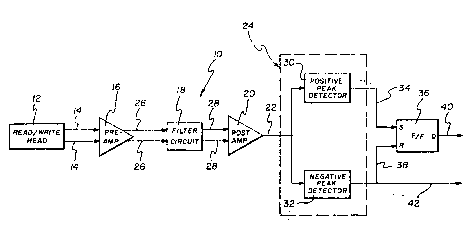
Attention is now directed to Fig. 1, which
shows an electrical circuit 10 of the present
invention. The structure of the circuit 10 is first
disclosed, followed by its operation.
Accordingly, the circuit 10 comprises a
magnetic read/write head 12. The head 12 reads an
encoded signal, as explained more fully below, and
outputs a read signal along a line pair-14.- The
read signal is amplified by a pre-amplifier 16,
filtéred by a filter circuit 18, again amplified by
a post-amplifier~20, and inputted along a line 22 to
a detector means 24. Appropriate line pairs for
,
processing the read signal are provided.by line
pairs 26, 2B.
The detector means 24, in turn, comprises a
positive threshold peak detector 30, and a negative
threshold peak detector 32 connected in parallel to
.
WO90/11~9 ~ v .~ PCT/US90/013~0
the positive threshold peak detector 30. The
positive threshold peak detector 30 outputs a first
pulse train signal, along a line 34, for input to a
set terminal tS) of a latch flip-flop 36; while the
negative threshold peak detector 32 outputs a second
pulse train signal, along a line 38, for input to a
reset terminal (R) of the flip-flop 36. The latch
flip-flop 36 further comprises an output terminal Q,
from which a logic signal can be outputted along a
line 40. The circuit lO is completed by noting a
means 42 for accessing the clock pulse train, for
reference against the logic signal on the line 40.
The operation of the Fig. l circuit lO will
now be disclosed, and reference additionally will be
made to the waveforms shown in Figs. 2A-D.
An objective of the operation of the
circuit lO is to decode binary data comprising first
and second information, which data has been encoded
into an encoded signal in accordance with the Chi
method, supra.
- An example of such an encoded signal, in
fact, a partial reproduction of the Chi Fig. l, is
shown in the present Fig. 2A. The encoded signal
comprises a succession of two event-cells, each of
which event-cells is demarcated by a pair of
negative clock transitions. Each event-cell is
dedicated-to encoding either a first or second
information. -In the Fig. 2A e~ample, the first
event-céll is dedicated to encoding a first ~
information that is a data 0; the second event-cell,
on the other hand, is dedicated to`encoding a second
information that is a data l. In particular, thè
data 0 is encoded by way of a first event comprising
three alternate information transitions at the
locations 4, 5, 6; and the data l is encoded by way
.... . . .
woso/ll~g PCT/US90/0l~0
Z~
--7--
of a second event comprising a single information
transition at the location 5.
The first and second events realize four
objectives in the encoding process: (1) they may
be located at any arbitrary location within an
event-cell; (2~ they operate to provide
discrimination of the first and second
informations; ~3) they leave invariant the
- negative clock transition polarity; and (4) they
operate, downstream, to generate first and second
read signal components.
This last point, on the first and second
read signal components, may be restated in the
following way. The encoded signal of Fig. 2A is
introduced to the Fig. 1 read/write head 12. The
head 12 reads the Fig. 2A encoded signal, and
produces a read signal (Fig. 2B) which corresponds
to a mathematical derivative of the encoded signal.
Therefore, the Fig. 2B read signal comprises a
succession of two event-cells, each of which
- event-cells comprises a pair of negative clock
transition components. Further, the read signal
comprises a first read signal component,
corresponding to, and derived from, the information
0 _ first event; the first read signal component~
having zero magnitude. Note that the first read
signal component has zero magnitude, because the
mathematical derivative of the three alternate
transitions, comprising the first event, is such as
to cancel out, in net, the alternate transitions
(see Chi, Fig. 2).
- - Similarly, the present Fig. 2B read~signal
comprises a second read signal component, --
corresponding to, and derived from, the information
1 --second event; the second read signal component
W~go/11~9 P~T/US90/01~0
~04'~33~
having a finite magnitude. Note that the second
read signal component has a finite magnitude,
because the mathematical derivative of the single
transition, comprising the second event, is such as
to produce a pulse of finite magnitude.
Continuing, the read signal comprising
clock transition components, and first and second
information components, as exemplified by Fig. 2B,
is introduced into the Fig. 1 electronics: the
pre-amplifier 16, the filter circuit 18, and the
post-amplifier 20, for input along the line 22 to
the detector means 24. For pedagogical purposes, it
is assumed that the input waveform to the detector
means 24, after the electronics, is substantially
equivalent to that already shown in Fig. 2~.
The detector means 24, by way of the
positive and negative threshold peak detectors 30,
32 respectively, interrogates the Fig. 2B read
signal for positive and negative peaks, and produces
separate first and second output signals. In
particular, the output of the negative threshold
peak detector 32, shown in Fig. 2C, is a first
output clock pulse train comprising the succession
of clock transition components; the output of the
2S positive threshold peak-detector 30, on the other
hand, is a second output information pulse train
(see Fig. 2C) comprising the first and second
information components.
- --Continuing,:the first clock pulse train
inputs along the line 38 to the reset terminal (R)
of the latch flip-flop 36, while the second
information pulse train-inputs along the line 34 to
the set terminal (S) of the flip-flop 36. The
flip-flop 36 responds to these inputs in the
following manner. Assume that a clock pulse is
WO 90tl 1~9 PCT/US90/01360
;r-t~
_g_
inputted to the reset terminal. Then, regardless of
whether the flip-flop 36 is in a logic 0 or logic 1
state, it outputs a logic 0 at the output terminal
Q, along the line 40. This is shown in Fig. 2D.
Now assume that an information pulse is inputted to
the set terminal. Then, regardless of whether the
flip-flop 36 is in a logic 0 or logic 1 state, it
outputs a logic 1 at the output terminal Q, along
the line 40. Again, see Fig. 2D.
Recall, in our running example, an
information 0 has been encoded in the first
event-cell, while an information 1 has been encoded
in the second event-cell (Fig. 2A). Fig. 2D shows
how this information has now been decoded. That is,
the first event-cell, defined by the first and
second clock pulses on the line 42, when mapped
against the output Q line 40, "sees" no pulse. By
definition, this means that the information 0 has
been encoded in the first event-cell. Similarly,
the second event-cell, defined by the second and
third clock pulses on the line 42, when mapped
against the output Q line 40, "sees" a transition or
flip-flop logic 1. By definition, this means that
the information 1 has been encoded in the second
event-cell.
Attention is now directed to Figs. 3A, B,
which show an alternative embodiment of the circuit
10. In particular, Fig. 3A shows a delay circuit 44
interposed between the clock pulse train on the line
38, and the reset terminal (R) of the flip-flop 36,
by way of a line 46. The delay circuit 44 can
comprise a series of inverters (not shown). Also
shown is the means 42 for accessing the clock pulse
train outputted by the negative peak detector 32, so
that this clock pulse train can be available as a
.~,
wo go/~ 1~9 2~ PCTtUS9~/013~0
--10--
reference against the logic state signal on the line
40. As explained above, the delay circuit 44
obviates a potential ambiguity that clock transition
components on Figs. 2D, could occur simultaneously,
hence ambiguously, with information components.
Fig. 3B may be compared to Fig. 2D, to show the
utility of the delay circuit 44 in avoiding the
potential ambiguity.
Finally, it is noted that this invention
makes use of e.g., read/write heads, flip-flops,
pre-amplifiers, etc. Conventional heads,
flip-flops, amplifiers, etc., can be used for this
purpose.
2S
3~
;, - ~ ''