Note : Les descriptions sont présentées dans la langue officielle dans laquelle elles ont été soumises.
2~5~240
The present invention relates to a method of print-
ing an image formed of 2-dimensionally arranged pixels,
and also to a printer such as an electronic photography
apparatus or a thermal printer, which is designed to
print an image formed of 2-dimensionally arranged
pixels.
A laser printer comprises a photosensitive
member and a laser diode. The laser diode is driven
in accordance with input image, thus emitting a laser
beam to the photosensitive member. The surface of the
photosensitive member is thereby scanned with the laser
beam.
An item of the image data, which represents a
pixel, is a signal S1 having the waveform shown in
Fig. 1. As is evident from Fig. 1, the signal Sl is at
either a high (H) level or a low (L) level for a period
Tl during which the photosensitive member is scanned to
form the pixel on its surface. The laser diode is
driven by a drive signal S2, which has the same wave
form as the image data signal S1 as is illustrated in
Fig. l. Hence, the laser diode emits a laser beam for
the period Tl, to form a pixel on the photosensitive
member.
The electric resistance at the surface of the
photosensitive member changes with the amount of light
applied to the member. The electric charge of the
surface of the member attenuates in accordance with the
~`
2~35~240
- 2 -
time the member is exposed to light. Hence, when the
laser diode is driven by the signal S2 (Fig. 1) and
emits a laser beam to the photosensitive member for
the period T1, a circular pixel will be formed on the
member, which circumscribes a square one-pixel region
as is shown at (a) in fig. 2.
When driven by two or more consecutive drive sig-
nals S2, the laser diode continuously emits a laser
beam to the photosensitive member, thereby forming
pixels which overlap one another as is shown at (b)
in Fig. 2. As can be understood from Fig. 2, these
overlapping pixels form a true black image since there
are left no blank spaces among them. Therefore, the
drive signals S2 are good for printing true black
images.
The drive signals S2 shown in Fig. 1 are far form
desirable for printing gray scale images by means of a
Bayer-type dither. Nor are they desirable for printing
characters, particularly complex ones (e.g.~ Chines
characters), each consisting of many strokes. When
driven by a signal S2, the laser diode emits a beam
for the period Tl, whereby a pixel will be formed which
circumscribes the one-pixel region. Hence, even if some
of consecutive drive signals S2 are at a low level as in
the case of printing a gray image or characters, the
resultant pixels overlap in most cases, as is illus-
trated at (c) in Fig. 2.
2~5~40
To print clear-cut gray images or characters, the
laser diode can be driven by a signal S3 which is at the
high level for a period T2 shorter than the period Tl as
is evident from Fig. 1. When driven by the signal S3,
the laser diode emits a laser beam to the photosensitive
member for the period T2, forming a pixel on the member.
This pixel is small, circumscribed by the square defin-
ing the one-pixel region as is shown at (a) in Fig. 3.
Hence, if some of consecutive drive signals S3 are at a
low level, the resultant pixels are discrete, forming a
clear-cut gray image or distinct characters as is illus-
trated at (b) in Fig. 3. Obviously, the drive signals
S3 are good for printing gray images and complex
characters.
The signals S3, which remain at the high level
for the period T2 (T2 < T1) are not good for printing
a true black image, however. When driven by two or
more consecutive drive signals S3, the laser diode
intermittently emits laser beams, each for the period
T2, thereby forming discrete pixels, with blank spaces
among them, as is illustrated at (c) in Fig. 3. The
discrete pixels, thus formed, fail to define a true
black image.
The above-described problem with the conventional
laser printer is also inherent in other types of
electrophotographic printers, such as a light-emitting
diode (LED) printer, a liquid-crystal printer. Further,
205~2~0
-- 4 --
the problem is found in thermal printers such as a heat-
transfer printer, ink-jet printers, and electrostatic
printers.
It is a first object of the invention to provide a
printer which can print not only a clear quasi-gray
image or clear characters, but also true black images,
either on different sheets of printing paper or on the
same sheet of printing paper.
It is a second object of the invention to provide a
method of printing not only a clear quasi-gray image or
clear characters, but also true black images, either on
different sheets of printing paper or on the same sheet
of printing paper.
To attain the first object, there is provided a
printer which comprises:
pixel-forming means for forming a number of pixels
on a printing medium, in accordance with image data con-
sisting of pixel-data items representing black pixels
and white pixels;
pixel-size setting means for setting a size for
a given black pixel to be formed, by determining the
values of pixel-data items representing consecutive
pixels arranged in a scanning direction and including
the given pixel; and
control means for controlling the pixel-forming
means, causing the pixel-forming means to form, on the
printing medium, the given pixel which has the size set
2û~0240
-- 5 --
by the pixel-size setting means.
Also, to achieve the first object, there is pro-
vided a printer which comprises:
pixel-forming means for forming a number of pixels
on a printing medium, in accordance with image data con-
sisting of pixel-data items representing black pixels
and white pixels;
pixel-size setting means for setting a size for
a given black pixel to be formed, by determining the
values of pixel-data items representing consecutive
pixels arranged in a direction perpendicular to a
scanning direction and including the given pixel; and
control means for controlling the pixel-forming
means, causing the pixel-forming means to form, on the
printing medium, the given pixel which has the size set
by the pixel-size setting means.
Further, in order to attain the first object, there
is provided a printer which comprises:
pixel-forming means for forming a number of pixels
on a printing medium, in accordance with image data con-
sisting of pixel-data items representing black pixels
and white pixels;
pixel-size setting means for setting a size for
a given black pixel to be formed, by determining the
values of pixel-data items representing consecutive
pixels arranged in a scanning direction and including
the given pixel, and the values of pixel-data items
205~?~0
representing consecutive pixels arranged in a direction
perpendicular to the scanning direction and including
the given pixel; and
control means for controlling the pixel-forming
means, causing the pixel-forming means to form, on the
printing medium, the given pixel which has the size set
by the pixel-size setting means.
Still further, in order to attain the first object,
there is provided a printer which comprises:
pixel-forming means for forming a number of pixels
on a printing medium, in accordance with image data con-
sisting of pixel-data items representing black pixels
and white pixels;
pixel-size setting means fo`r setting a size for
a given black pixel to be formed, by determining the
values of pixel-data items representing consecutive
pixels arranged in a scanning direction and including
the given pixel, the values of pixel-data items repre-
senting consecutive pixels arranged in a direction
perpendicular to the scanning direction and including
the given pixel, and the values of pixel-data items rep-
resenting consecutive pixels arranged in a direction
oblique to the scanning direction and including the
given pixel; and
control means for controlling the pixel-forming
means, causing the pixel-forming means to form, on the
printing medium, the given pixel which has the size set
205D240
by the pixel-size setting means.
To accomplish the second object of the invention,
there is provided a method of printing images by means
of pixel-forming means, comprising the steps of:
receiving image data consisting of pixel-data items
representing black and white pixels arranged;
setting a size for a given black pixel to be
formed, by determining the values of pixel-data items
representing consecutive pixels arranged in a scanning
direction and including the given pixel; and
controlling the pixel-forming means, causing the
same to form, on the printing medium, the given pixel
which has said size.
To accomplish the second object of the invention,
too, there is provided a method of printing images by
means of pixel-forming means, comprising the steps of:
receiving image data consisting of pixel-data items
representing black and white pixels arranged;
setting a size for a given black pixel to be
formed, by determining the values of pixel-data items
representing consecutive pixels arranged in a direction
perpendicular to a scanning direction and including the
given pixel; and
controlling the pixel-forming means, causing the
same to form, on the printing medium, the given pixel
which has said size.
Also, in order to achieve the second object of the
205t~24 0
invention, there is provided a method of printing images
by means of pixel-forming means, comprising the steps
of:
receiving image data consisting of pixel-data items
representing black and white pixels arranged;
setting a size for a given black pixel to be
formed, by determining the values of pixel-data items
representing consecutive pixels arranged in a scanning
direction and including the given pixel, and the values
of pixel-data items representing consecutive pixels
arranged in a direction perpendicular to the scanning
direction and including the given pixel; and
controlling the pixel-forming means, causing the
same to form, on the printing medium, the given pixel
which has said size.
Moreover, to attain the second object of the
invention, there is provided a method of printing images
by means of pixel-forming means, comprising the steps
of:
receiving image data consisting of pixel-data items
representing black and white pixels arranged;
setting a size for a given black pixel to be
formed, by determining the values of pixel-data items
representing consecutive pixels arranged in a scanning
direction and including the given pixel, the values of
pixel-data items representing consecutive pixels
arranged in a direction perpendicular to the scanning
2~0240
direction and including the given pixel, and the values
of pixel-data items representing consecutive pixels
arranged in a direction oblique to the scanning direc-
tion and including the given pixels; and
controlling the pixel-forming means, causing the
same to form, on the printing medium, the given pixel
which has said size.
This invention can be more fully understood from
the following detailed description when taken in con-
junction with the accompanying drawings, in which:
Fig. 1 is a timing chart showing the image-data
signals, laser-driving signals of one type, and laser-
driving signals of another type -- all used in a conven-
tional laser printer;
Fig. 2 shows various pixel-patterns which the con-
ventional laser printer forms when laser-driving signals
of the first type are used;
Fig. 3 shows various pixel patterns which the con-
ventional laser printer forms when laser-driving signals
of the second type are used;
Fig. 4 is a block diagram illustrating a laser
printer which is a first embodiment of the present
invention;
Fig. 5 shows 3-pixel patterns which can be detected
by the emission-time setting section incorporated in the
laser printer of Fig. 4;
Fig. 6 is a timing chart showing the pixel signals,
20502~0
- 10 -
emission-time setting signals, and laser-driving
signals -- all used in the printer shown in Fig. 4;
Fig. 7 represents the pixel pattern formed by the
printer of Fig. 4 and defining a true black image;
Fig. 8 is a block diagram illustrating a thermal
printer which is a second embodiment of the present
invention;
Fig. 9 is a timing chart showing latch signals and
enable signals, which are used in the thermal printer
shown in Fig. 8;
Fig. 10 is a block diagram showing another laser
printer which is a third embodiment of the present
invention;
Fig. 11 schematically represents the data table
used in the emission-time setting section of the printer
shown in Fig. 10;
Fig. 12 shows 3-pixel patterns which can be
detected by the emission-time setting section of the
laser printer illustrated in Fig. 10;
Fig. 13 is a timing chart showing the pixel
signals, emission-time setting signals, and laser-
driving signals -- all used in the printer shown in
Fig. 10;
Fig. 14 shows various pixel patterns which the
printer of Fig. 10 forms;
Fig. 15 represents a pixel pattern formed by the
printer of Fig. 10 and defining a true black image;
2050240
Fig. 16 is a block diagram showing another thermal
printer which is a fourth embodiment of the present
invention;
Fig. 17 is a timing chart showing latch signals and
enable signals, which are used in the thermal printer
illustrated in Fig. 16;
Fig. 18 is a block diagram showing still another
laser printer which is a fifth embodiment of this
invention;
Fig. 19 schematically shows the data table used in
the emission-time setting section of the printer shown
in Fig. 18;
Fig. 20 represents a variety of pixel-patterns
which the emission-time setting section of the printer
shown in Fig. 18 can detect;
Fig. 21 is a timing chart showing the pixel
signals, emission-time setting signals, and laser-
driving signals -- all used in the printer of Fig. 18;
Fig. 22 is a diagram showing various pixel patterns
which the printer of Fig. 18 can form;
Fig. 23 represents a pixel pattern formed by the
printer of Fig. 18 and defining a true black image;
Fig. 24 is a block diagram illustrating still
another thermal printer which is a sixth embodiment of
the present invention;
Fig. 25 is a timing chart showing latch signals and
enable signals, which are used in the thermal printer
2 0 ~ 4 0
- 12 -
illustrated in Fig. 24;
Fig. 26 is a block diagram showing a laser printer
according to a seventh embodiment of the invention;
Fig. 27 is a schematic representation of the data
table used in the emission-time section of the laser
beam printer shown in Fig. 26;
Fig. 28 is a timing chart showing the pixel
signals, emission-time setting signals, and laser-
driving signals -- all used in the printer of Fig. 26
to print images;
Fig. 29 illustrates pixels of various sizes which
the printer of Fig. 26 can form on a printing medium;
Fig. 30 represents a pixel pattern formed by
the printer of Fig. 26 and defining a true black
15 image;
Fig. 31 is a block diagram showing a thermal
printer which is an eighth embodiment of the invention;
Fig. 32 is a timing chart showing latch signals and
enable signals, which are used in the thermal printer
20 illustrated in Fig. 31;
Fig. 33 is a block diagram illustrating another
laser printer which is the ninth embodiment of the
present invention;
Fig. 34 schematically shows a pixel pattern which
25 the printer of Fig. 33 can detects;
Fig. 35 is a schematic representation of the data
table used in the emission-time setting section of the
- 13 - 20~0.~40
laser printer illustrated in Fig. 33; and
Fig. 36 shows laser-driving signals having differ-
ent durations, which are used in the printer of Fig. 34
to print images.
Embodiments of the present invention will now be
described, with reference to the accompanying drawings.
First Embodiment
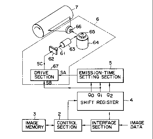
Fig. 4 illustrates a laser printer according to
the first embodiment of the invention. As is shown
in Fig. 4, the laser printer comprises an interface
section l, a control section 2, an image memory 3, a
shift register 4, an emission-time setting section 5,
and a laser scanner unit (LSU) 6, and a photosensitive
drum 7.
The interface section l transfers image data
between the control section 2 and an external device
(not shown). (When the laser printer is incorporated
in a facsimile apparatus, the section l transfers the
image data between the section 2 and the data receiving/
transmitting section of the facsimile apparatus.)
The control section 2 supplies the image data to
the image memory 3. The memory 3 has storage capacity
great enough to store at least one page of data. Every
time the memory 3 stores one page of data, the one-page
data is read from the memory 3 and supplied to the shift
register 4 under the control of the control section 2.
The shift register 4 is a 3-bit one, which shifts
2 ~ 4 0
- 14 -
the input data, bit by bit, in response to the pulses
forming the image data, which are used as transfer clock
pulses. The shift register 4 outputs three bits Qo, Ql
and Q2 simultaneously to the emission-time setting sec-
tion 5. In other words, the register samples everythree bits of the image data, which represents three
consecutive pixels to be formed on the photosensitive
drum 7 and be aligned in the horizontal direction, i.e.,
the direction of the main scanning of the drum 7.
The bit Ql is supplied to the LSU 6 as pixel signal
representing the pixel corresponding to the bit Ql
The emission-time setting section 5 has a ROM (not
shown) storing data items showing reference 3-bit pat
terns. The section 5 detects a 3-pixel patterns from
the values of the three bits Qo, Ql and Q2 supplied from
the shift register 4, and outputs an emission-time sig-
nal SA to the LSU 6. The signal SA represents the time
for which the LSU 6 is driven to print the pixel corre-
sponding to the bit Ql
As is evident from Fig. 4, the LSU 6 comprises a
laser diode 62, a collimator lens 63, an electric motor
64, a polygon mirror 65, an f-0 lens 66, a drive sec-
tion 67. Upon receipt of the pixel signal SB from the
shift register 4, the drive section 67 outputs a drive
signal SC which is a pulse having the width correspond-
ing the emission time represented by the signal SA out-
put by the time-emission setting section 5. The drive
2~240
- 15 -
signal SC is supplied to the laser diode 62. Driven by
the signal SC, the diode 62 emits a laser beam 61 for
the time set by the section 5. The beam 61 is applied
to the collimator lens 63, which converges the beam 61
into a laser beam having a predetermined diameter. The
beam from the collimator 63 is applied to the polygon
mirror 65 being rotated by the motor 64 at a constant
speed. The mirror 65 reflects the beam and applies it
to the f-~ lens 66. The lens 66 applies the beam to
the photosensitive drum 7, achieving a uniform-speed
scanning of the drum 7 and forming a latent pixel image
on the drum 7.
various devices (not shown), such as a drum-
charging device, an image-developing device, an
image-transferring device, an image-fixing device, a
drum-cleaning device -- all being of the known types --
are located around the photosensitive drum 7. Equipped
with these devices, the laser printer shown in Fig. 4 is
an electrophotographic printer of so-called "reverse
developing type."
The operation of the laser printer will now be
explained, with reference to Figs. 5, 6 and 7.
First, the image data stored in the image memory 3
is input to the shift register 4, bit by bit, under the
control of the control section 2. Every time the image
data is shifted by one bit in the register 4, three
consecutive bits Qo, Ql and Q2 are supplied to the
20~a~4~
emission-time setting section 5, and the bit Ql is sup-
plied as a pixel signal SB to the drive section 67.
Whenever the bit Ql is "1," thus representing a
black pixel, the emission-time setting section 5 detects
the 3-pixel pattern defined by the bits Qo, Ql and Q2,
from the values of these bits Qo, Ql and Q2 which repre-
sents three consecutive pixels arranged in the horizon-
tal direction (i.e., the main scanning direction). When
the bit Ql is "1," the three bits Qo, Ql and Q2 can
0 define the following four 3-pixel patterns:
Pattern 1: Only the middle pixel is black, as is
shown at (a) in Fig. 5.
Pattern 2: The middle and left pixels are black,
as is shown at (b) in Fig. 5.
Pattern 3: The middle and right pixels are black,
as is shown at (c) in Fig. 5.
Pattern 4: All three pixels are black, as is shown
at (d) in Fig. 5.
When the section 5 detects the 3-pixel pattern 1,
it outputs a signal SA representing a beam-emission
period TA. When it detects the 3-pixel pattern 2 or 3,
it generates a signal SA representing a beam-emission
period TB. When it detects the 3-pixel pattern 4, it
outputs a signal SA representing a beam-emission period
TC
As is shown in Fig. 6, the drive section 67
outputs, in response to the signal SA representing
- 17 - 2 ~ ~ ~ 2 4 0
the period TA, a drive signal SC which is at a high
level for the period TA; it outputs, in response to the
signal SA representing the period TB, a drive signal SC
which is at a high level for the period TB; it outputs,
in response to the signal SA showing the period Tc, a
drive signal SC which is at a high level for the period
TC- Here, TA < TB < TC < Tl- The period TC is equal
to a one-pixel scanning period Tl in the present
embodiments.
When driven for the shortest period TA, the laser
diode 62 emits a laser beam for this period TA, whereby
a pixel is formed on the drum 7, which is small and
located well within the one-pixel region. When driven
for the longer period TB, the laser diode 62 emits a
laser beam for the period TB, whereby a pixel is formed
on the drum 7, which is circumscribed by the one-pixel
region, as is shown in at (a) in Fig. 3. When driven
for the longest period Tc, the laser diode 62 emits a
laser beam for this period TC, whereby a pixel is formed
on the drum 7, which is large, circumscribing the one-
pixel region, as is shown at (a) in Fig. 2.
To print a quasi-gray image or complex characters,
which are defined by discrete black pixels, the laser
diode 62 is repeatedly driven, each time for the period
TA or TB and emitting a laser beam for this period,
whereby discrete black pixels, each located well within
or circumscribed by the one-pixel region, are formed
2 ~ 4 0
- 18 -
ultimately on a printing medium. The black pixels, thus
formed, define a clear-cut quasi-gray image or distinct
characters.
On the other hand, to print a true black image,
which is defined by overlapping black pixels, the laser
diode 62 is repeatedly driven, each time for the period
TC (i.e., one-pixel scanning period Tl) and emitting for
the period TC, whereby black pixels, each circumscribing
the one-pixel region and overlapping another, are formed
ultimately on a printing medium. The black pixels, thus
formed, define a true black image.
A pattern of three consecutive pixels is recognized
in the present embodiment. Then when either one of right
and left side pixels in the pattern having more than three
consecutive pixels is detected, the condition of the end
pixels is discriminated as two consecutive black pixels.
As a result, a black pixel of which size is smaller than
that obtained in three consecutive pixels is formed,
thereby obtaining a true black image of Fig. 7 as appar-
ent from Fig. 7, the size of the black pixels at rightand left side is smaller than that of the other black
pixels. In such an image, the boundary between the true
black image and white portion surrounding the two black
image can be clearly recognized when it is observed by
eyes. The printed condition can, therefore, be improved.
Second Embodiment
Fig. 8 illustrates a thermal printer which is
20~0~40
- 19 -
a second embodiment of the present invention. As Fig. 8
shows, the thermal printer comprises a head controller
10, an enable signal generator 20, an image data proc-
essing section 30, a head driver 40, and a thermal print
head 50.
The head controller 10 is connected to an external
device (not shown). (When the thermal printer is incor-
porated in a facsimile apparatus, the head controller 10
is connected to the image data between the section 2 and
the data receiving/transmitting section of the facsimile
apparatus.) The head controller 10 receives image data
from the external device and supplies the data to the
image data processing section 30. It generates timing
signals, latch signals, and clock signals -- all syn-
chronous with the pixel signals forming the image data.The timing signals are supplied to the enable signal
generator 20. The latch signals and the clock signals
are supplied to the image data processing section 30.
The enable signal generator 20 generates enable
signals from the timing signals produced by the head
controller 10, and supplies the enable signals (later
described) to the head driver 40.
The image processing section 30 comprises a shift
register 31, a power-supply time setting device 32, a
line memory 33, and an output controller 34. The shift
register 31 is a 3-bit register, and shifts the input
data, bit by bit, in response to the pulses forming the
2 0 ~ 0
- 20 -
image data, which are used as transfer clock pulses.
The shift register 4 outputs three bits Qo, Ql and Q2
simultaneously to the power-supply time setting device
32. In other words, the shift register 31 samples every
three bits of the image data, which represents three
consecutive pixels to be formed on a printing medium
and be aligned in the horizontal direction. The power-
supply time setting device 32 has a ROM, and outputs a
3-bit data item consisting of the bits Qo, Ql and Q2
simultaneously output from the shift register 31. The
3-bit data item is stored into the line memory 33. The
line memory 33 has capacity of storing n 3-bit data
items, where n is the number of pixels forming one
horizontal line. The output controller 34 controls the
line memory 33 in accordance with the clock signal and
the latch signal supplied from the head controller 10,
causing the line memory 33 to output pixel bits, one by
one.
The head driver 40 comprises a shift register 41, a
latch circuit 42, two-input AND gates 43-1, 43-2,
43-n, and switching amplifiers 44-1, 44-2, ..., 44-n.
The register 41 is an n-bit shift register. It holds
and shifts the pixel bits output by the line memory 33,
and supplies n pixel bits Q0 to Qn simultaneously to the
latch circuit 42 in response to a clock signal CK sup-
plied from the head controller 10. The latch circuit 42
receives and holds the n pixel bits Q0 to Qn supplied
20~240
from the shift register 41, in response to a latch sig-
nal LA supplied from the head controller lO. The pixel
bits Q0 to Qn are output from the latch circuit 42 and
supplied to the AND gates 43-1 to 43-n, respectively, at
their first input terminals. The other input terminal
of each AND gate is coupled to the enable signal genera-
tor 20, thus receiving the enable signal EN therefrom.
The outputs of the AND gates 43-1 to 43-n are connected
to the switching amplifiers 44-1 to 44-n, respectively.
Hence, the AND gates 43-l to 43-n supply the pixel bits
Q0 to Qn to the switching amplifiers 44-l to 44-n,
respectively, only while the enable signal EN remains at
a high level. The outputs of the switching amplifiers
44-l to 44-n are connected to the heating resistors R-l
to R-n incorporated in the thermal print head 50. Each
switching amplifier applies a voltage of 24v to the
heating resistor as long as the input signal remains at
the high level.
The operation of the thermal printer shown in
Fig. 8 will now be explained, with reference to the
timing chart of Fig. 9.
First, image data is supplied from the external
device to the head controller lO. The head controller
lO supplies the image data to the image data processing
section 30, and generates a timing signal, a clock
signal CK, and a latch signal LA. The timing signal
is input to the enable signal generator 20, the clock
2~50240
signal CK is supplied to the output controller 34 and
the shift register 41, and the latch circuit LA is sup-
plied to the output controller 34 and the latch circuit
42.
Upon receipt of the timing signal, the enable
signal generator 20 generates an enable signal EN.
The enable signal EN is supplied to the second input
terminals of the AND gates 43-1 to 43-n.
In the image processing section 30, the shift
register 31 outputs three bits Qo, Ql and Q2 for each
pixel bit, simultaneously, to the power-supply time
setting device 32. These bits Qo, Ql and Q2 represent
three consecutive pixels to be formed on a printing
medium and be aligned in the horizontal direction.
The power-supply time setting device 32 outputs a 3-bit
data item which represents the combination of the bits
Q0~ Ql and Q2, in terms of the values thereof. More
specifically, the device 32 produces 3-bit data items
in the following scheme:
1. When the bits Qo, Ql and Q2 are "0", "1" and
"0", respectively, the device 32 produces a
3-bit data of "001."
2. When the bits Qo, Ql and Q2 are "1", "1" and
"0", respectively, the device 32 produces a
3-bit data of "010."
3. When the bits Qo, Ql and Q2 are "0", "1" and
"1", respectively, the device 32 produces
2 9 5 9 ~ 4 ~
a 3-bit data of "010."
4. When the bits Qo, Ql and Q2 are "1", "1" and
"1", respectively, the device 32 produces a
3-bit data of "100."
5. When the bit Ql is "0", the device 32 produces
a 3-bit data of "000."
The 3-bit data item is stored into the line memory
33. As the shift register 31 sequentially inputs other
3-bit pixel data items, each consisting of the bits Q0,
Ql and Q2, to the power-supply time setting device 32,
the device 32 outputs other 3-bit data items, each for
one pixel bit. These 3-bit data items are stored into
the line memory 33, one after another.
In accordance with the clock signal CK, the output
controller 34 control the line memory 33, whereby only
the first bit (i.e.~ the least significant bit) of each
3-bit data item is read from the memory 33. The first
bit of each 3-bit data item is supplied to the head
driver 40.
In the head driver 40, n bits read from the line
memory 33, each being the first bit of each 3-bit data
item, are stored into the shift register 41, one after
another, during the period I as is shown in Fig. 9.
When the last of these n bits is stored into the regis-
ter 41, the head controller 10 outputs a latch signal
pulse II having a predetermined width, as can be under-
stood from Fig. 9. This pulse II is supplied to the
2~0 -~40
- 24 -
latch circuit 42 and also to the output controller 34.
In response to the pulse II, the latch circuit 42
receives and holds the n bits from the shift register
41.
In response to the latch signal pulse II, the out-
put controller 34 controls the line memory 33, whereby
only the second bit (i.e., the second least significant
bit) of each 3-bit data item is read from the memory 33.
AS a result, n bits, each being the second bit of each
3-bit data item stored in the memory 33, are input to
the shift register 41, one after another, during the
period III as is shown in Fig. 9.
The enable signal generator 20 generates an enable
signal pulse in response to the timing signal supplied
from the head controller 10, upon lapse of a predeter-
mined time from the trailing edge of each latch signal
pulse, as can be understood from Fig. 9. Hence, the
generator 20 generates an enable signal pulse IV having
a width TA upon lapse of said time from the trailing
edge of the latch signal pulse II. This pulse IV is
supplied to the second input terminal of each AND gate.
In the meantime, the n bits Q0 to Qn held in the
latch circuit 42, each being the first bit of each 3-bit
data item stored in the line memory 33, are input to the
AND gates 43-1 to 43-n, respectively. Hence, any AND
gate, whose first input terminal receives a "1" bit
which indicates that only the middle of the three
2~S3240
- 25 -
consecutive pixels is black, is on for the period TA,
i.e., the width of the enable signal pulse IV. As a
result, the switching amplifier coupled to such AND gate
is turned on for the same period TA, applying the volt-
age (24v) to the corresponding heating resistor of thethermal print head 50.
When the last of the n bits, each being the second
bit of each 3-bit data item stored in the line memory
33, is input to the shift register 41, the head control-
ler 10 outputs a latch signal pulse V as is shown inFig. 9. The pulse v is supplied to the output control-
ler 34 and the latch circuit 41. In response to this
pulse V, the latch circuit 42 receives and holds the n
bits from the shift register 41.
In response to the latch signal pulse v, the output
controller 34 controls the line memory 33, whereby only
the third bit (i.e., the most significant bit) of each
3-bit data item is read from the memory 33. As a
result, n bits, each being the third bit of each 3-bit
data item stored in the memory 33, are input to the
shift register 41, one after another, during the period
VI as is shown in Fig. 9.
Upon lapse of the predetermined time from the
trailing edge of the latch signal pulse v, the generator
20 generates an enable signal pulse VII having a width
TB. This pulse VII is supplied to the second input ter-
minal of each AND gate.
2U~,74~
- 26 -
Meanwhile, the n bits Q0 to Qn held in the latch
circuit 42, each being the second bit of each 3-bit
data item stored in the line memory 33, are input to the
AND gates 43-1 to 43-n, respectively. Hence, any AND
gate, whose first input terminal receives a "1" bit
which indicates that the middle and left or right of
the three consecutive pixels are black, is on for the
period TB, i.e., the width of the enable signal pulse
VII. The switching amplifier coupled to such AND gate
is thereby turned on for the same period TB, applying
the voltage (24V) to the corresponding heating resistor
of the thermal print head 50.
When the last of the n bits, each being the third
bit of each 3-bit data item stored in the line memory
33, is input to the shift register 41, the head control-
ler 10 outputs a latch signal pulse vIII as is shown
in Fig. 9. The pulse VIII is supplied to the output
controller 34 and the latch circuit 41. In response to
this pulse VIII, the latch circuit 42 receives and
holds the n bits from the shift register 41.
In response to the latch signal pulse VIII, the
output controller 34 controls the line memory 33,
whereby only the first bit (i.e., the least significant
bit) of each 3-bit data item of the next one-line data
is read from the memory 33. As a result, n bits, each
being the first bit of each 3-bit data item stored in
the memory 33, are input to the shift register 41, one
2~532 i(~
after another.
Upon lapse of the predetermined time from the
trailing edge of the latch signal pulse VIII, the
generator 20 generates an enable signal pulse XI having
a width Tc. This pulse XI is supplied to the second
input terminal of each AND gate.
In the meantime, the n bits Q0 to Qn held in the
latch circuit 42, each being the third bit of each 3-bit
data item stored in the line memory 33, are input to
the AND gates 43-1 to 43-n, respectively. Hence, any
AND gate, whose first input terminal receives a "1" bit
which indicates that the three consecutive pixels are
black, is on for the period Tc, i.e., the width of the
enable signal pulse XI. The switching amplifier coupled
to such AND gate is thereby turned on for the same
period Tc applying the voltage (24V) to the correspond-
ing heating resistor of the thermal print head 50.
The enable signal generator 20 cyclically gener-
ates three pulses having widths TA, TB and Tc, where
TA < TB ~ TC- The widths TA, TB and Tc defines periods
TA, TB and TC~ during which the heating the switching
amplifiers 44-1 to 44-n apply the drive voltage to the
heating resistors R-l to R-n of the thermal print head
50.
The image data processing section 30 processes
other one-line data items sequentially supplied from the
head controller 10, in the specific way explained above.
2 ~ 4 0
- 28 -
The head driver 40 drives the thermal print head 50 in
the manner described above, in accordance with the sig-
nals CK and LA supplied from the head controller 10 and
also in accordance with the enable signals EN generated
by the enable signal generator 20.
As has been described, the 3-bit data output by
the power-supply time setting section 32 is "001" when
only the middle one of three consecutive pixels is
black, is "010" when the middle one and left or right
one of three consecutive pixels are black, is "100" when
all consecutive three pixels are black, and is "000"
when the middle one of the three consecutive pixels is
white. In other words, only the first bit of the 3-bit
data output by the device 32 is "1" when the middle
pixel is black, only the second bit thereof is "1" when
the middle pixel and the left or right pixel are black,
only the third bit thereof is "1" when all three pixels
are black, and none of the three bits are "1" when the
middle pixel is white.
Thus, when only the middle pixel is black, the
heating resistor is driven for the period TA, printing
a small black pixel located well within the one-pixel
region. When the middle pixel and the left for right
pixel are black, the heating resistor is driven for the
period TB longer than the period TA, thereby printing a
black pixel circumscribed by the one-pixel region, as is
shown at (a) in fig. 3. When all three pixels are
2 a ~ Y~ o
- 29 -
black, the heating resistor is driven for the period Tc
longer than the period TB, thus printing a black pixel
circumscribing the one-pixel region, as is illustrated
at (a) in Fig. 2. When the middle pixel is white, no
voltage is applied to the heating resistor since none of
the three bits are "1," and the resistor prints no black
pixel.
When the heating resistors R-1 to R-n are repeat-
edly driven, each time for the period TA or TB, discrete
black pixels, each located well within or circumscribed
by the one-pixel region, will be formed on a printing
medium, defining a clear-cut quasi-gray image or dis-
tinct characters.
on the other hand, when the heating resistors R-l
to R-n are repeatedly driven, each time for the period
TC, overlapping black pixels, each circumscribing the
one-pixel region, will be formed on a printing medium,
defining a true black image.
Third Embodiment
Fig. 10 illustrates a laser printer which is a
third embodiment of the present invention and which
is similar to the laser printer shown in Fig. 4. Some
of the components of this printer, which are identical
to those shown in Fig. 4 are designated at the same
numerals in Fig. 10 and will not be described in
detail.
As is evident from Fig. 10, the laser printer
2 ~ !~ D ~
- 30 -
comprises an interface section 1, a control section 2,
an image memory 3, a laser scanner unit (LSU) 6, a pho-
tosensitive drum 7, three shift registers 104a, lOb and
104c, and an emission-time setting section 105.
The shift registers 104a, 104b and 104c are each an
n-bit shift register, where n is the number of pixels
which form a one-line image. They shift the input data,
bit by bit, in response to the transfer clock pulses,
i.e., the pulses forming the image data supplied to the
interface section 1. These registers 104a, 104b and
104c are connected in series. Hence, the output of the
register 104a is input to the register 104b, and the
output of the register 104b is input to the register
104c. Every time the one-line image data items are
shifted by one bit in the registers 104a, 104b and
104c, these registers output three bits QA, QB and QC~
respectively. These three bits represent three consec-
utive pixels to be printed in the vertical direction,
i.e., the sub-scanning direction. In other words, the
shift registers 104a, 104b and 104c cooperate to sample
every three bits of the image data, which represent
three consecutive pixels to be formed on the photosensi-
tive drum 7 and be aligned in the vertical direction, or
the direction of the sub-scanning of the drum 7.
The three bits QA, QB and QC output from the regis-
ters 104a, 104b and 104c, respectively, are supplied to
the emission-time setting section 105. Of these three
20~0~,740
bits, the bit QB, i.e., the output of the register 104b,
is supplied to the drive section 67 of the LSU 6 since
the output of the register 104b is connected to the
drive section 67.
The emission-time setting section 105 has a ROM
(not shown) storing the data table shown in Fig. 11.
The section 5 detects one of the four 3-pixel patterns
shown in Fig. 12, from the values of the three bits QA,
QB and QC supplied from the shift registers 104a, 104b
and 104c, and outputs an emission-time signal SA to the
LSU 6. The signal SA represents the time for which the
LSU 6 is driven to print the pixel corresponding to the
bit QB-
As in the laser beam shown in Fig. 4, various
devices (not shown), such as a drum-charging device, an
image-developing device, an image-transferring device,
an image-fixing device, a drum-cleaning device -- all
being of the known types -- are located around the pho-
tosensitive drum 7.
The operation of the laser printer shown in Fig. 10
will now be explained, with reference to Fig. 11 through
Fig. 15.
At first, the shift registers 104a, 104b and 104c
are empty. Then, the image data is supplied to the
shift register 104a, hence to the shift register 104b,
and further to the shift register 104c. Thus, the image
data is shifted, bit by bit, through the registers 104a,
2û~ 40
- 32 -
104b and 104c under the control of the control section
2. AS has been described, the shift registers 104a,
104b and 104c are each an n-bit register, capable of
storing a one-line data, and are connected in series.
Hence, when the shift register 104a starts receiving the
third one-line data, the shift register 104b starts
outputting the first one-line data to the drive section
67, bit by bit, each being being a pixel SB.
The drive section 67 drives the laser diode 62
incorporated in the LSU 6 in accordance with the data
output from the shift register 104b. Meanwhile, the
emission-time setting section 105 receives the three
bits QA, QB and QC from the registers 104a, 104b and
104c, detects the 3-pixel pattern from these bits QA, QB
and QC, and and output an emission-time signal SA which
corresponds to one of the data items stored in the ROM.
The signal SA is supplied to the drive section 67.
More specifically, the emission-time setting sec-
tion 105 detects the 3-pixel pattern defined by the bits
QA~ QB and QC~ from the values of these bits which rep-
resents three consecutive pixels arranged in the verti-
cal direction (i.e., the sub-scanning direction). When
the bit QB is "1," the three bits QA, QB and QC can
define the following four 3-pixel patterns:
Pattern 1: Only the middle pixel is black, as is
shown at (a) in Fig. 12.
Pattern 2: The middle and upper pixels are black,
~0240
as is shown at (b) in Fig. 12.
Pattern 3: The middle and lower pixels are black,
as is shown at (c) in Fig. 12.
Pattern 4: All three pixels are black, as is shown
at (d) in Fig. 12.
When the section 105 detects the 3-pixel pattern l,
it data item A (Fig. ll) and outputs a signal SA repre-
senting a beam-emission period TA. When it detects
the 3-pixel pattern 2 or 3, it selects data item B and
generates a signal SA representing a beam-emission
period TB. When it detects the 3-pixel pattern 4, it
selects data item C and outputs a signal SA representing
a beam-emission period Tc.
As is shown in Fig. 13, the drive section 67
outputs, in response to the signal SA representing the
period TA, a drive signal SC which is at a high level
for the period TA; it outputs, in response to the signal
SA representing the period TB, a drive signal SC which
is at a high level for the period TB; it outputs, in
response to the signal SA showing the period Tc, a
drive signal SC which is at a high level for the period
Tc. Here, TA < TB ~ TC S Tl. The period Tc is equal to
a one-pixel scanning period Tl in the present
embodiments.
When driven for the shortest period TA, the laser
diode 62 emits a laser beam for this period TA, whereby
a pixel is formed on the drum 7, which is small and
2 ~ 4 0
- 34 -
located well within the one-pixel region as is shown at
(a) in Fig. 14. When driven for the longer period TB,
the laser diode 62 emits a laser beam for the period TB,
whereby a pixel is formed on the drum 7, which is cir-
cumscribed by the one-pixel region, as is shown in at
(b) in Fig. 14. When driven for the longest period Tc,
the laser diode 62 emits a laser beam for this period
Tc, whereby a pixel is formed on the drum 7, which is
large, circumscribing the one-pixel region, as is shown
at (c) in Fig. 14.
To print a quasi-gray image or complex characters,
which are defined by discrete black pixels, the laser
diode 62 is repeatedly driven, each time for the period
TA or TB and emitting a laser beam for this period,
whereby discrete black pixels, each located well within
or circumscribed by the one-pixel region, are formed
ultimately on a printing medium. The black pixels, thus
formed, define a clear-cut quasi-gray image or distinct
characters.
On the other hand, to print a true black image,
which is defined by overlapping black pixels, the laser
diode 62 is repeatedly driven, each time for the period
TC (i-e-~ one-pixel scanning period Tl) and emitting for
the period Tc, whereby black pixels, each circumscribing
the one-pixel region and overlapping another, are formed
ultimately on a printing medium. The black pixels, thus
formed, define a true black image.
2 ~ 50 ~ 4 0
A pattern of three consecutive pixels is recognized
in the present embodiment. Then when either one of
upper and lower side pixels in the pattern having more
than three consecutive pixels is detected, the condition
of the end pixels is discriminated as two consecutive
black pixels. As a result, a black pixel of which size
is smaller than that obtained in three consecutive
pixels is formed, thereby obtaining a true black image
of Fig. 15 as apparent from Fig. 15, the size of the
black pixels at upper and lower side is smaller than
that of the other black pixels. In such as image,
the boundary between the true black image and white
portion surrounding the two black image can be clearly
recognized when it is observed by eyes. The printed
lS condition can, therefore, be improved.
Fourth Embodiment
Fig. 16 illustrates a thermal printer which is a
fourth embodiment of the present invention. As Fig. 16
shows, the thermal printer comprises a head controller
10, an enable signal generator 20, a head driver 40, a
thermal print head 50, and an image data processing sec-
tion 130. All the components, except for the section
130, are identical in both structure and function to
those designated at the same reference numerals in
Fig. 8.
The image processing section 130 comprises three
shift registers 131a, 131b, 131c, a power-supply time
2Q5~0
- 36 -
setting device 132, a line memory 133, and an output
controller 134.
The shift registers 131a, 131b and 131c are each an
n-bit shift register, where n is the number of pixels
which form a one-line image. They shift the input data,
bit by bit, in response to the transfer clock pulses,
i.e., the pulses forming the image data supplied from
the head controller 10. These registers 131a, 131b and
131c are connected in series. Hence, the output of the
register 131a is input to the register 131b, and the
output of the register 131b is input to the register
131c. Every time the one-line image data items are
shifted by one bit in the registers 131a, 131b and
131c, these registers output three bits QA, QB and QC~
respectively. These three bits represent three consecu-
tive pixels to be printed in the vertical direction,
i.e., the sub-scanning direction. In other words, the
shift registers 131a, 131b and 131c cooperate to sample
every three bits of the image data, which represent
three consecutive pixels to be formed on a printing
medium and be aligned in the vertical direction, or the
direction of the sub-scanning.
The three bits QA, QB and QC output from the
registers 131a, 131b and 131c, respectively, are sup-
plied to the power-supply time setting device 132.
The power-supply time setting device 132 has a ROM
(not shown), and outputs a 3-bit data item consisting of
2û~0240
- 37 -
the bits QA, QB and QC output from the shift registers
131a, 131b and 131c. The 3-bit data item is stored into
the line memory 133. The line memory 133 has capacity
of n 3-bit data items, where n is the number of pixels
forming one horizontal line. The output controller 134
controls the line memory 133 in accordance with the
clock signal and the latch signal supplied from the head
controller 10, causing the line memory 133 to output
pixel bits, one by one.
The operation of the thermal printer shown in
Fig. 16 will now be explained, with reference to the
timing chart of Fig. 17.
First, image data is supplied from the external
device to the head controller 10. The head controller
10 supplies the image data to the image data processing
section 130, and generates a timing signal, a clock
signal CK, and a latch signal LA. The timing signal
is input to the enable signal generator 20, the clock
signal CK is supplied to the output controller 134 and
the shift register 41 incorporated in the head driver
40, and the latch circuit LA is supplied to the output
controller 134 and the latch circuit 42 incorporated in
the head driver 40.
Upon receipt of the timing signal, the enable
signal generator 20 generates an enable signal EN.
The enable signal EN is supplied to the second input
terminals of the AND gates 43-1 to 43-n incorporated in
20~240
- 38 -
the head driver 40.
In the image processing section 130, the shift reg-
isters 131a, 131b and 131c output three bits QA, QB and
QC for each pixel bit, to the power-supply time setting
device 132. These bits QA ~ QB and QC represent three
consecutive pixels to be formed on a printing medium and
be aligned in the vertical direction, i.e., sub-scanning
direction. The power-supply time setting device 132
outputs a 3-bit data item which represents the combina-
tion of the bits Qo, Ql and Q2, in terms of the values
thereof. More specifically, the device 132 produces
3-bit data items in the following scheme:
1. When the three bits are "0", "1" and "0", indicat-
ing that only the middle pixel is black as is shown
at (a) in Fig. 12, the device 132 produces a 3-bit
data of "001."
2. When the three bits are "1", "1" and "0", indicat-
ing that the middle and upper pixels are black as
is shown at (b) in Fig. 12, the device 132 produces
a 3-bit data of "010."
3. When the three bits are "0", "1" and "1", indicat-
ing that the middle and the lower pixels are black
as is shown at (c) in Fig. 12, the device 132 pro-
duces a 3-bit data of "010."
4. when the three bits are "1", "1" and "1", indicat-
ing that all three pixels are black as is shown at
(d) in Fig. 12, the device 132 produces a 3-bit
4 0
- 39 -
data of "100."
5. When the bit QB is "0", indicating that the middle
pixel is white, the device 132 produces a 3-bit data
of "000."
The 3-bit data item is stored into the line memory
133. As each of the shift registers 131a, 131b and 131c
sequentially inputs other bits to the power-supply time
setting device 132, the device 132 outputs other 3-bit
data items, each for one pixel bit. These 3-bit data
items are stored into the line memory 133, one after
another.
In accordance with the clock signal CK, the output
controller 134 control the line memory 133, whereby only
the first bit (i.e., the least significant bit) of each
3-bit data item is read from the memory 133. The first
bit of each 3-bit data item is supplied to the head
driver 40.
In the head driver 40, n bits read from the line
memory 133, each being the first bit of each 3-bit data
item, are stored into the shift register 41, one after
another, during the period I as is shown in Fig. 17.
When the last of these n bits is stored into the regis-
ter 41, the head controller 10 outputs a latch signal
pulse II having a predetermined width, as can be under-
stood from Fig. 9. This pulse II is supplied to the
latch circuit 42 and also to the output controller 134.
In response to the pulse II, the latch circuit 42
2 Q ~ o ? ~ o
- 40 -
receives and holds the n bits from the shift register
41.
In response to the latch signal pulse II, the out-
put controller 134 controls the line memory 133, whereby
only the second bit (i.e.~ the second least significant
bit) of each 3-bit data item is read from the memory
133. As a result, n bits, each being the second bit of
each 3-bit data item stored in the memory 133, are input
to the shift register 41, one after another, during the
period III as is shown in Fig. 17.
The enable signal generator 20 generates an enable
signal pulse in response to the timing signal supplied
from the head controller 10, upon lapse of a predeter-
mined time from the trailing edge of each latch signal
pulse, as can be understood from Fig. 17. Hence, the
generator 20 generates an enable signal pulse IV having
a width TA upon lapse of said time from the trailing
edge of the latch signal pulse II. This pulse IV is
supplied to the second input terminal of each AND gate.
In the meantime, the n bits Q0 to Qn held in the
latch circuit 42, each being the first bit of each 3-bit
data item stored in the line memory 133, are input to
the AND gates 43-1 to 43-n, respectively. Hence, any
AND gate, whose first input terminal receives a "1" bit
which indicates that only the middle of the three con-
secutive pixels is black, is on for the period TA, i.e.,
the width of the enable signal pulse IV. As a result,
2 ~ o
- 41 -
the switching amplifier coupled to such AND gate is
turned on for the same period TA, applying the voltage
(24V) to the corresponding heating resistor of the ther-
mal print head 50.
When the last of the n bits, each being the second
bit of each 3-bit data item stored in the line memory
133, is input to the shift register 41, the head con-
troller 10 outputs a latch signal pulse V as is shown
in Fig. 17. The pulse V is supplied to the output con-
troller 134 and the latch circuit 41. In response to
this pulse V, the latch circuit 42 receives and holds
the n bits from the shift register 41.
In response to the latch signal pulse v, the output
controller 134 controls the line memory 133, whereby
only the third bit (i.e., the most significant bit) of
each 3-bit data item is read from the memory 133. As a
result, n bits, each being the third bit of each 3-bit
data item stored in the memory 133, are input to the
shift register 41, one after another, during the period
VI as is shown in Fig. 17.
Upon lapse of the predetermined time from the
trailing edge of the latch signal pulse v, the generator
20 generates an enable signal pulse vII having a width
TB. This pulse VII is supplied to the second input
terminal of each AND gate.
Meanwhile, the n bits Q0 to Qn held in the latch
circuit 42, each being the second bit of each 3-bit data
2 ~ 0
- 42 -
item stored in the line memory 133, are input to the AND
gates 43-1 to 43-n, respectively. Hence, any AND gate,
whose first input terminal receives a "1" bit which
indicates that the middle and left or right of the three
consecutive pixels are black, is on for the period TB,
i.e., the width of the enable signal pulse VII. The
switching amplifier coupled to such AND gate is thereby
turned on for the same period TB, applying the voltage
(24V) to the corresponding heating resistor of the ther-
mal print head 50.
When the last of the n bits, each being the third
bit of each 3-bit data item stored in the line memory
133, is input to the shift register 41, the head con-
troller 10 outputs a latch signal pulse VIII as is shown
in Fig. 17. The pulse VIII is supplied to the output
controller 134 and the latch circuit 41. In response to
this pulse VIII, the latch circuit 42 receives and holds
the n bits from the shift register 41.
In response to the latch signal pulse VIII, the
output controller 134 controls the line memory 133,
whereby only the first bit (i.e., the least significant
bit) of each 3-bit data item of the next one-line data
is read from the memory 133. As a result, n bits, each
being the first bit of each 3-bit data item stored in
the memory 133, are input to the shift register 41, one
after another.
Upon lapse of the predetermined time from the
23~ 40
- 43 -
trailing edge of the latch signal pulse VIII, the gener-
ator 20 generates an enable signal pulse XI having a
width TC This pulse XI is supplied to the second input
terminal of each AND gate.
In the meantime, the n bits Q0 to Qn held in the
latch circuit 42, each being the third bit of each 3-bit
data item stored in the line memory 133, are input to
the AND gates 43-1 to 43-n, respectively. Hence, any
AND gate, whose first input terminal receives a "1" bit
which indicates that the three consecutive pixels are
black, is on for the period Tc, i.e., the width of the
enable signal pulse XI. The switching amplifier coupled
to such AND gate is thereby turned on for the same
period Tc applying the voltage (24V) to the correspond-
ing heating resistor of the thermal print head 50.
The enable signal generator 20 cyclically gener-
ates three pulses having widths TA, TB and Tc, where
TA < TB < TC- The widths TA, TB and Tc defines periods
TA, TB and Tc, during which the heating the switching
amplifiers 44-1 to 44-n apply the drive voltage to the
heating resistors R-l to R-n of the thermal print head
50.
The image data processing section 130 processes
other one-line data items sequentially supplied from the
head controller 10, in the specific way explained above.
The head driver 40 drives the thermal print head 50 in
the manner described above, in accordance with the
%~S~240
signals CK and LA supplied from the head controller 10
and also in accordance with the enable signals EN gener-
ated by the enable signal generator 20.
As has been described, the 3-bit data output by the
power-supply time setting device 132 is "001" when only
the middle one of three consecutive pixels is black, is
"010" when the middle one and left or right one of three
consecutive pixels are black, is "100" when all consecu-
tive three pixels are black, and is "000" when the mid-
dle one of the three consecutive pixels is white. In
other words, only the first bit of the 3-bit data output
by the device 132 is "1" when the middle pixel is black,
only the second bit thereof is "1" when the middle pixel
and the left or right pixel are black, only the third
bit thereof is "1" when all three pixels are black, and
none of the three bits are "1" when the middle pixel is
white.
Thus, when only the middle pixel is black, the
heating resistor is driven for the period TA, printing a
small black pixel located well within the one-pixel
region. When the middle pixel and the left for right
pixel are black, the heating resistor is driven for the
period TB longer than the period TA, thereby printing
a black pixel circumscribed by the one-pixel region, as
is shown at (a) in Fig. 3. When all three pixels are
black, the heating resistor is driven for the period Tc
longer than the period TB, thus printing a black pixel
205~40
- 45 -
circumscribing the one-pixel region, as is illustrated
at (a) in Fig. 2. When the middle pixel is white, no
voltage is applied to the heating resistor since none of
the three bits are "1," and the resistor prints no black
pixel.
When the heating resistors R-l to R-n are repeat-
edly driven, each time for the period TA or TB, discrete
black pixels, each located well within or circumscribed
by the one-pixel region, will be formed on a printing
medium, defining a clear-cut quasi-gray image or
distinct characters.
On the other hand, when the heating resistors R-l
to R-n are repeatedly driven, each time for the period
Tc, overlapping black pixels, each circumscribing the
one-pixel region, will be formed on a printing medium,
defining a true black image.
Fifth Embodiment
Fig. 18 illustrates a laser printer which is a
fifth embodiment of the invention and which is similar
to the laser printer shown in Fig. 4. Some of the
components of this printer, which are identical to those
shown in Fig. 4 are designated at the same numerals in
Fig. 18 and will not be described in detail.
As is evident from Fig. 18, the laser printer
comprises an interface section 1, a control section 2,
an image memory 3, a laser scanner unit (LSU) 6, a pho-
tosensitive drum 7, three shift registers 204a, 204b and
2~3~240
- 46 -
204c, and an emission-time setting section 205.
As in the laser beam shown in Fig. 4, various
devices (not shown)~ such as a drum-charging device, an
image-developing device, an image-transferring device,
an image-fixing device, a drum-cleaning device -- all
being of the known types -- are located around the
photosensitive drum 7.
The shift registers 204a, 204b and 204c are each an
n-bit shift register, where m is the number of pixels
which form a one-line image. They shift the input data,
bit by bit, in response to the transfer clock pulses,
i.e., the pulses forming the image data supplied from
the control section 2. These registers 204a, 204b and
204c are connected in series. Hence, the output of the
register 204a is input to the register 204b, and the
output of the register 204b is input to the register
204c. Every time the one-line image data items are
shifted by one bit in the registers 204a, 204b and 204c,
these registers output three bits QA, QB and QC,
respectively, and the registers 204b and 204c outputs
two bits QD and QE which immediately follows and pre-
cedes the bit QB, respectively. The bits QA, QB and QC
represent three consecutive pixels to be printed in the
vertical direction, i.e., the sub-scanning direction.
On the other hand, the bits QB~ QD and QE represents
three consecutive pixels to be printed in the horizontal
direction, i.e., the main scanning direction. The five
2~5~5~40
- 47 -
pixels represented by the five bits QA~ QB~ QC~ QD and
QE form a cross, the center of which is defined by the
bits QB. In other words, the shift registers 204a, 204b
and 204c cooperate to sample every five bits of the
image data, which represent a cross to be printed on a
printing medium.
These five bits QA~ QB, QC~ QD and QE are sup-
plied from the shift registers 294a, 204b and 204c to
the emission-time setting section 205. Further, of
these five bits, the bit QB is supplied to the drive
section 67 incorporated in the LSU 6, as a pixel signal
representing a pixel to be printed.
The emission-time setting section 205 has a ROM
tnot shown) which stores the data table shown in
Fig. 19. It detects one of the sixteen 5-pixel patterns
shown in Fig. 19, from the values of the bits QA~ QB~
QC~ QD and QE output from the shift registers 204a, 204b
and 204c, and outputs an emission-time signal SA to the
LSU 6. The signal SA represents the time for which the
LSU 6 is driven to print the pixel corresponding to the
bit QB-
As in the laser beam shown in Fig. 4, various
devices (not shown)~ such as a drum-charging device, an
image-developing device, an image-transferring device,
an image-fixing device, a drum-cleaning device -- all
being of the known types -- are located around the
photosensitive drum 7.
2~S0240
- 48 -
The operation of the laser printer shown in Fig. 18
will now be explained, with reference to Fig. 19 through
Fig. 23.
At first, the shift registers 204a, 204b and 204c
are empty. Then, the image data is supplied to the
shift register 204a, hence to the shift register 204b,
and further to the shift register 204c. Thus, the image
data is shifted, bit by bit, through the registers 204a,
204b and 204c under the control of the control section
2. As has been described, the shift registers 204a,
204b and 204c are each an n-bit register, capable of
storing a one-line data, and are connected in series.
Hence, when the shift register 204a starts receiving the
third one-line data, the shift register 204b outputs the
first bit QB f the first one-line data to the drive
section 67, as pixel signal SB.
The drive section 67 drives the laser diode 62
incorporated in the LSU 6 in response to the pixel sig-
nal SB. Meanwhile, the emission-time setting section
205 receives the five bits QA, QB, QC, QD and QE from
the registers 204a, 204b and 204c, detects the 5-pixel
pattern from these five bits and outputs an emission-
time signal SA which corresponds to one of the data
items stored in the ROM. The signal SA is supplied to
the drive section 67.
More specifically, the emission-time setting sec-
tion 205 detects the 5-pixel pattern defined by the bits
2~240
- 49 -
QA, QB, QC~ QD and QE from the values of these bits
which represents five pixels arranged in the form of a
cross, the center of which is the pixel represented by
the bit QB. When the bit QB is "1," the three bits QA,
QB and QC can define the sixteen 5-pixel patterns (a) to
(p) which are illustrated in Fig. 20 which are stored in
the ROM. The 5-pixel patterns are classified into the
following three types:
Type A: Only the center pixel is black, or the
center pixel and only another pixel is
black.
Type B: The center pixel and two or three other
pixels are black.
Type C: A11 five pixels are black.
When the section 105 detects a 5-pixel pattern of
type A, it outputs an emission-time signal SA represent-
ing a beam-emission period TA. When it detects a
5-pixel pattern of type B, it generates an emission-time
signal SA representing a beam-emission period TB. When
it detects the 5-pixel pattern C, it outputs an
emission-time signal SA representing a beam-emission
period Tc.
AS is shown in the timing chart of Fig. 21, the
drive section 67 outputs a drive signal SC which is at a
high level for the period TA~ in response to the signal
SA representing the period TA; it outputs, a drive sig-
nal SC which is at a high level for the period TB, in
2 Q ~ ~ !~ 4 ~
- 50 -
response to the signal SA representing the period TB; it
outputs, a drive signal SC which is at a high level for
the period Tc, in response to the signal SA showing the
period Tc. Here, TA < TB < Tc- The period Tc is equal
to a one-pixel scanning period Tl.
The drive signal SC is supplied to the laser diode
62 of the LSU 6, thus driving the laser diode 62. When
driven for the shortest period TA, the laser diode 62
emits a laser beam for this period TA, whereby a pixel
represented by the signal Ss is formed on the drum 7,
which is small and circumscribed by the one-pixel region
as is shown at DA to DL in Fig. 22. When driven for the
longer period TB, the laser diode 62 emits a laser beam
for the period TB, whereby a pixel represented by the
signal SB is formed on the drum 7, which has a diameter
longer than the side of the one-pixel region but not
long enough to circumscribe the region, as is shown at
DM and DN in Fig. 22. When driven for the longest
period Tc, the laser diode 62 emits a laser beam for
this period Tc, whereby a pixel is formed on the drum 7,
which is large, circumscribing the one-pixel region, as
is shown at DO in Fig. 14.
To print a quasi-gray image or complex characters,
which are defined by discrete black pixels, the laser
diode 62 is repeatedly driven, each time for the period
TA or TB and emitting a laser beam for this period,
whereby discrete black pixels, each circumscribed by
2~i01~0
the one-pixel region or having a diameter longer than
the side of the one-pixel region but not long enough to
circumscribe the region, are formed ultimately on a
printing medium. The black pixels, thus formed, define
a clear-cut quasi-gray image or distinct characters.
On the other hand, to print a true black image,
which is defined by overlapping black pixels, the laser
diode 62 is repeatedly driven, each time for the period
TC (i.e., one-pixel scanning period Tl) and emitting for
the period TC, whereby black pixels, each circumscribing
the one-pixel region and overlapping another, are formed
ultimately on a recording medium. The black pixels,
thus formed, define a true black image.
As has been described, the laser diode 62 is driven
for the period Tc and forms a large pixel when the five
bits QA, QB, QC, QD and QE supplied from the shift reg-
isters 204a, 204b and 204c are all "1," each represent-
ing a black pixel, and is driven for the shorter period
TA or TB and forms a smaller pixel when any one of the
five bits, except the bits QB is "0," representing a
white pixel. Hence, there can be printed a clearly
outlined, true black image, as can be understood from
Fig. 23.
Sixth Embodiment
Fig. 24 illustrates a thermal printer which is a
sixth embodiment of the present invention. As Fig. 24
shows, the thermal printer comprises a head controller
20~2~0
- 52 -
10, an enable signal generator 20, a head driver 40, a
thermal print head 50, and an image data processing sec-
tion 230. A11 the components, except for the section
230, are identical in both structure and function to
those designated at the same reference numerals in
Fig. 8.
The image processing section 230 comprises three
shift registers 231a, 231b, 231c, a power-supply time
setting device 232, a line memory 233, and an output
lo controller 234.
The shift registers 231a, 231b and 231c are each an
n-bit shift register, where n is the number of pixels
which form a one-line image. They shift the input data,
bit by bit, in response to the transfer clock pulses,
i.e., the pulses forming the image data supplied from
the head controller 10. These registers 231a, 231b and
231c are connected in series. Hence, the output of the
register 231a is input to the register 131b, and the
output of the register 131b is input to the register
131c. Every time the one-line image data items are
shifted by one bit in the registers 231a, 231b and 231c,
these registers output three bits QA, QB and QC~
respectively, and the registers 231b and 231c outputs
two bits QD and QE which immediately follows and pre-
cedes the bit QB~ respectively. The bits QA~ QB and QC
represent three consecutive pixels to be printed in the
vertical direction, i.e., the sub-scanning direction.
2 ~ 4 0
On the other hand, the bits QB, QD and QE represents
three consecutive pixels to be printed in the horizontal
direction, i.e., the main scanning direction. The five
pixels represented by the five bits QA~ QB~ QC~ QD and
QE form a cross, the center of which is defined by the
bits QB. In other words, the shift registers 231a, 231b
and 231c cooperate to sample every five bits of the
image data, which represent a cross to be printed on a
printing medium.
The five bits QA, QB, QC~ QD and QE S imultaneously
output from the registers 231a, 231b and 231c are sup-
plied to the power-supply time setting device 232.
The power-supply time setting device 232 has a ROM
(not shown), and outputs a 3-bit data item upon receipt
of the five bits QA, QB, QC~ QD and QE S imultaneously
output from the registers 231a, 231b and 231c. The
3-bit data item is stored into the line memory 233.
The line memory 233 has capacity of n 3-bit data items,
where n is the number of pixels forming one horizontal
line. The output controller 234 controls the line
memory 233 in accordance with the clock signal and the
latch signal supplied from the head controller 10,
causing the line memory 233 to output pixel bits, one
by one, as will be explained below in detail.
The operation of the thermal printer shown in
Fig. 24 will now be explained, with reference to the
timing chart of Fig. 25.
2 ~ . o
First, image data is supplied from the external
device to the head controller 10. The head controller
10 supplies the image data to the image data processing
section 230, and generates a timing signal, a clock
signal CK, and a latch signal LA. The timing signal
is input to the enable signal generator 20, the clock
signal CK is supplied to the output controller 234 and
the shift register 41 incorporated in the head driver
40, and the latch circuit LA is supplied to the output
controller 234 and the latch circuit 42 incorporated in
the head driver 40.
Upon receipt of the timing signal, the enable
signal generator 20 generates an enable signal EN.
The enable signal EN is supplied to the second input
terminals of the AND gates 43-1 to 43-n incorporated in
the had driver 40.
In the image processing section 230, the shift reg-
isters 231a, 231b and 231c simultaneously output five
bits QA~ QB, QC~ QD and QE. These five bits represent
five pixels forming a cross, the bits QA, QB and QC
representing three consecutive pixels arranged in the
vertical direction (i.e.~ sub-scanning direction), the
bits QD, QB and QE representing three consecutive pixels
arranged in the horizontal direction (i.e., main scan-
ning direction), and the bit QB representing the centerpixel to be printed on a printing medium. The power-
supply time setting device 232 outputs a 3-bit data
2~2~0
item the value of which is determined from the values
of the five bits QA, QB, QC~ QD and QE S imultaneously
output from the registers 231a, 231b and 231c. More
specifically, the device 232 produces 3-bit data items
in the following scheme:
1. When only the bit QB represents a black pixel as
is shown at (a) in Fig. 20, or when the bit QB
and another bit represent black pixels as is shown
at (b) to (e)~ the device 232 produces a 3-bit data
of "001."
2. When the bit QB and two or three other bits repre-
sent black pixels as is shown at (f) to (o) in
Fig. 20, the device 232 produces a 3-bit data of
"010. "
3. When 211 five bits QA, QB, QC~ QD and QE represent
black pixels as is shown at (p) in Fig. 20, the
device 232 produces a 3-bit data of "100."
4. When the QB represents a white pixel, the device
232 produces a 3-bit data of "000."
The 3-bit data item is stored into the line memory
233. AS each of the shift registers 231a, 231b and 231c
sequentially inputs other bits to the power-supply time
setting device 232, the device 232 outputs other 3-bit
data items, each for one pixel bit QB. These 3-bit data
items are stored into the line memory 233, one after
another.
In accordance with the clock signal CK, the output
20~0~0
- 56 -
controller 234 control the line memory 233, whereby only
the first bit (i.e., the least significant bit) of each
3-bit data item is read from the memory 233. The first
bit of each 3-bit data item is supplied to the head
driver 40.
In the head driver 40, n bits read from the line
memory 233, each being the first bit of each 3-bit data
item, are stored into the shift register 41, one after
another, during the period I as is shown in the timing
chart of Fig. 25. When the last of these n bits is
stored into the register 41, the head controller 10
outputs a latch signal pulse II having a predetermined
width, as can be understood from Fig. 25. This pulse II
is supplied to the latch circuit 42 and also to the out-
put controller 234. In response to the pulse II, thelatch circuit 42 receives and holds the n bits from the
shift register 41.
In response to the latch signal pulse II, the out-
put controller 234 controls the line memory 233, whereby
only the second bit (i.e.~ the second least significant
bit) of each 3-bit data item is read from the memory
233. As a result, n bits, each being the second bit of
each 3-bit data item stored in the memory 233, are input
to the shift register 41, one after another, during the
period III as is shown in Fig. 25.
The enable signal generator 20 generates an enable
signal pulse in response to the timing signal supplied
205~240
from the head controller 10, upon lapse of a predeter
mined time from the trailing edge of each latch signal
pulse, as can be understood from Fig. 25. Hence, the
generator 20 generates an enable signal pulse IV having
a width TA upon lapse of said time from the trailing
edge of the latch signal pulse II. This pulse IV is
supplied to the second input terminal of each AND
gate.
In the meantime, the n bits Q0 to Qn held in the
latch circuit 42, each being the first bit of each 3-bit
data item stored in the line memory 233, are input to
the AND gates 43-1 to 43-n, respectively. Hence, any
AND gate, whose first input terminal receives a "1" bit
which indicates that only the middle of the three con-
secutive pixels is black, is on for the period TA, i. e.,the width of the enable signal pulse IV. AS a result,
the switching amplifier coupled to such AND gate is
turned on for the same period TA, applying the voltage
(24V) to the corresponding heating resistor of the
thermal print head 50.
When the last of the n bits, each being the second
bit of each 3-bit data item stored in the line memory
233, is input to the shift register 41, the head con-
troller 10 outputs a latch signal pulse V as is shown
in Fig. 25. The pulse v is supplied to the output con-
troller 234 and the latch circuit 41. In response to
this pulse v, the latch circuit 42 receives and holds
2 û ~ 4 0
- 58 -
the n bits from the shift register 41.
In response to the latch signal pulse V, the output
controller 234 controls the line memory 233, whereby
only the third bit (i.e., the most significant bit) of
each 3-bit data item is read from the memory 233. AS a
result, n bits, each being the third bit of each 3-bit
data item stored in the memory 233, are input to the
shift register 41, one after another, during the period
VI as is shown in the timing chart of Fig. 25.
Upon lapse of the predetermined time from the
trailing edge of the latch signal pulse V, the generator
20 generates an enable signal pulse VII having a width
TB. This pulse VII is supplied to the second input
terminal of each AND gate.
Meanwhile, the n bits Q0 to Qn held in the latch
circuit 42, each being the second bit of each 3-bit data
item stored in the line memory 33, are input to the AND
gates 43-1 to 43-n, respectively. Hence, any AND gate,
whose first input terminal receives a "1" bit which
indicates that the middle and left or right of the three
consecutive pixels are black, is on for the period TB,
i.e., the width of the enable signal pulse VII. The
switching amplifier coupled to such AND gate is thereby
turned on for the same period TB, applying the voltage
(24v) to the corresponding heating resistor of the ther-
mal print head 50.
When the last of the n bits, each being the third
- 59 _ 2 OS 0240
bit of each 3-bit data item stored in the line memory
233, is input to the shift register 41, the head con-
troller 10 outputs a latch signal pulse VIII as is
shown in Fig. 25. The pulse VIII is supplied to the
output controller 234 and the latch circuit 41. In
response to this pulse VIII, the latch circuit 42
receives and holds the n bits from the shift register
41.
In response to the latch signal pulse VIII, the
output controller 234 controls the line memory 233,
whereby only the first bit (i.e., the least significant
bit) of each 3-bit data item of the next one-line data
is read from the memory 233. AS a result, n bits, each
being the first bit of each 3-bit data item stored in
the memory 233, are input to the shift register 41, one
after another.
Upon lapse of the predetermined time from the
trailing edge of the latch signal pulse VIII, the
generator 20 generates an enable signal pulse XI having
a width Tc. This pulse XI is supplied to the second
input terminal of each AND gate.
In the meantime, the n bits Q0 to Qn held in the
latch circuit 42, each being the third bit of each 3-bit
data item stored in the line memory 233, are input to
the AND gates 43-1 to 43-n, respectively. Hence, any
AND gate, whose first input terminal receives a "1" bit
which indicates that the three consecutive pixels are
- 60 -
black, is on for the period Tc, i.e., the width of the
enable signal pulse XI. The switching amplifier coupled
to such AND gate is thereby turned on for the same
period Tc applying the voltage (24v) to the correspond-
ing heating resistor of the thermal print head 50.
The enable signal generator 20 cyclically generates
three pulses having widths TA, TB and Tc, where
TA < TB < TC- The widths TA, TB and Tc defines periods
TA, TB and Tc, during which the heating the switching
amplifiers 44-l to 44-n apply the drive voltage to the
heating resistors R-l to R-n of the thermal print head
50.
The image data processing section 230 processes any
other one-line data items sequentially supplied from the
head controller 10, three data items at a time, in the
specific way explained above. The head driver 40 drives
the thermal print head 50 in the manner described above,
in accordance with the signals CK and LA supplied from
the head controller 10 and also in accordance with the
enable signals EN generated by the enable signal genera-
tor 20.
As has been described, the 3-bit data output by the
power-supply time setting section 232 is "001" when only
the middle one of the five pixels forming a cross is
black or when the middle one and another of the five
pixels are black, is "010" when the middle one and two
or three others of the five pixels are black, is "100"
20~0~40
- 61 -
when all five pixels are black, and is "000" when the
middle one of the three consecutive pixels is white. In
other words, only the first bit of the 3-bit data output
by the device 132 is "1" when the middle pixel is black
or when the middle pixel and another adjacent pixel are
black, only the second bit thereof is "1" when the mid-
dle pixel and two or three adjacent pixels are black,
only the third bit thereof is "1" when all five pixels
are black, and none of the three bits are "1" when the
o middle pixel is white.
Thus, when only the middle pixel is black or when
the middle pixel and another pixel are black, the heat-
ing resistor is driven for the period T A , printing a
small black pixel (DA or DC in Fig. 22) circumscribed by
the one-pixel region. When the middle pixel and two or
three adjacent pixels are black, the heating resistor is
driven for the period TB longer than the period TA,
thereby printing a black pixel (DM or DN in Fig. 22)
having a diameter longer than the wide of the one-pixel
region but not long enough to circumscribe the region.
When all three pixels are black, the heating resistor is
driven for the period Tc longer than the period TB, thus
printing a black pixel (DO in Fig. 22) circumscribing
the one-pixel region. When the middle pixel is white,
no voltage is applied to the heating resistor since none
of the three bits are "1," and the resistor prints no
black pixel.
2~2~0
- 62 -
When the heating resistors R-l to R-n are repeat-
edly driven, each time for the period TA or TB, discrete
black pixels, each located well within or circumscribed
by the one-pixel region, will be formed on a printing
s medium, defining a clear-cut quasi-gray image or dis-
tinct characters.
On the other hand, when the heating resistors R-l
to R-n are repeatedly driven, each time for the period
Tc, overlapping black pixels, each circumscribing the
one-pixel region, will be formed on a printing medium,
defining a true black image.
Seventh Embodiment
Fig. 26 illustrates a laser printer which is a
seventh embodiment of the invention and which is similar
to the laser printer shown in Fig. 4. Some of the com-
ponents of this printer, which are identical to those
shown in Fig. 4 are designated at the same numerals in
Fig. 26 and will not be described in detail.
As is evident from Fig. 26, the laser printer
comprises an interface section 1, a control section 2,
an image memory 3, a laser scanner unit (LSU) 6, a
photosensitive drum 7, three shift registers 304a, 304b
and 304c, and an emission-time setting section 305.
As in the laser beam shown in Fig. 4, various
devices (not shown), such as a drum-charging device, an
image-developing device, an image-transferring device,
an image-fixing device, a drum-cleaning device -- all
2û~02~0
- 63 -
being of the known types -- are located around the
photosensitive drum 7.
The shift registers 304a, 304b and 304c are each an
n-bit shift register, where n is the number of pixels
which form a one-line image. They shift the input data,
bit by bit, in response to the transfer clock pulses,
i.e., the pulses forming the image data supplied from
the control section 2. These registers 304a, 304b and
304c are connected in series. Hence, the output of the
register 304a is input to the register 304b, and the
output of the register 304b is input to the register
304c. Every time the registers 304a, 304b and 304c
shift the one-line image data items by one bit, they
output three bits QA, QB and QC, respectively. At the
same time, the register 304a also outputs two bits QE
and QD which follows the bit QA, the register 304b
also outputs two bits QG and QF which follows the bit
QB, and the register 304c also outputs two bits QI and
QH which follows the bit QC, as can be understood from
Fig. 26.
The three bits QA, QE and QD simultaneously output
from the shift register 304a represent three consecutive
ones of the pixels forming a first horizontal line,
i.e., the pixels arranged in the main scanning line.
The three bits QB~ QG and QF output from the shift
register 304b represent three consecutive ones of the
pixels forming a second horizontal line, i.e., the
2 ~S O ~ 4 0
- 64 -
pixels arranged in the main scanning line. The three
bits QC, QI and QH output from the shift register 304c
represent three consecutive ones of the pixels forming a
third horizontal line, i.e., the pixels arranged in the
main scanning line. Since the shift registers 304a,
304b and 304c, each holding a one-line data item, are
connected in series, the bits QA, QB and QC output from
the registers 304a, 304b and 304c, represent three con-
secutive pixels arranged in the vertical direction,
i.e., the sub-scanning direction; the bits QE, QG and QI
output from the registers 304a, 304b and 304c, represent
three consecutive pixels arranged in the vertical
direction; and the bits QD, QF and QH output from the
registers 304a, 304b and 304c, represent three consecu-
tive pixels arranged in the vertical direction. Hence,the nine bits QA to QI represent a 3 x 3 pixel matrix of
the type illustrated in Fig. 27, the bit QG representing
the center pixel of the 3 x 3 matrix. In other words,
the shift registers 304a, 304b, and 304c cooperate to
sample every nine bits of the image data, which repre-
sent a 3 x 3 pixel matrix.
These nine bits QA to QI are supplied from the
shift registers 304a, 304b and 304c to the emission-time
setting section 205. Further, of these five bits, the
bit QG is supplied to the drive section 67 incorporated
in the LSU 6, as a pixel signal representing a pixel to
be printed.
2 ~ 0
- 65 -
The emission-time setting section 205 has a ROM
(not shown) which stores a data table showing various
g-bit patterns and three periods TA, TB and Tc. It
detects one of the various patterns which the bits QA
to QI define when the bit QG represents a black pixel,
in accordance with the values of the bits QA to QI
output from the shift registers 304a, 304b and 304c.
Then, it outputs an emission-time signal SA to the LSU
6. The signal SA represents the time for which the
LSU 6 is driven to print the pixel corresponding to the
bit QG-
As in the laser beam shown in Fig. 4, various
devices (not shown), such as a drum-charging device, an
image-developing device, an image-transferring device,
an image-fixing device, a drum-cleaning device -- all
being of the known types -- are located around the
photosensitive drum 7.
The operation of the laser printer shown in Fig. 26
will now be explained, with reference to Figs. 28, 29
and 30. At first, the shift registers 304a, 304b and
304c are empty. Then, the image data is supplied to the
shift register 304a, hence to the shift register 304b,
and further to the shift register 304c. Thus, the image
data is shifted, bit by bit, through the registers 304a,
304b and 304c under the control of the control section
2. As has been described, the shift registers 304a,
304b and 304c are each an n-bit register, capable of
20~2~0
- 66 -
storing a one-line data, and are connected in series.
Hence, when the shift register 304a receives the last
bit of the second one-line data, the shift register 304b
outputs the bit QG, which is supplied to the drive sec-
tion 67, as pixel signal SB.
The drive section 67 drives the laser diode 62
incorporated in the LSU 6 in response to the pixel sig-
nal SB. Meanwhile, the emission-time setting section
305 receives the five nine QA to QI from the registers
304a, 304b and 304c, detects the 9-pixel pattern from
these nine bits, and outputs an emission-time signal SA
which represents of the periods TA~ TB and Tc stored in
the ROM. The signal SA is supplied to the drive section
67.
More specifically, the emission-time setting sec-
tion 305 detects the 9-pixel pattern defined by the bits
QA to QI, from the values of these bits which represents
nine pixels forming a 3x 3 matrix, the center of which
is the pixel represented by the bit QG. When the bit QG
is "1," the nine bits QA to QI can define 256-pixel pat-
terns (= 28 patterns) which are stored in the ROM. The
9-pixel patterns are classified into the following three
types:
Type A: Only the center pixel is black, or the cen-
ter pixel and only another pixel is black.
Type B: The center pixel and three to five other
pixels are black.
2û~0~0
- 67 -
Type C: The center pixel and six to eight other
pixels are black.
When the section 205 detects a 9-pixel pattern of
type A, it outputs an emission-time signal SA represent-
ing a beam-emission period TA. When it detects a
9-pixel pattern of type B, it generates an emission-time
signal SA representing a beam-emission period TB. When
it detects the 9-pixel pattern of pattern C, it outputs
an emission-time signal SA representing a beam-emission
period Tc.
AS is shown in the timing chart of Fig. 28, the
drive section 67 outputs a drive signal SC which is
at a high level for the period TA, in response to the
signal SA representing the period TA; it outputs, a
drive signal SC which is at a high level for the period
TB, in response to the signal SA representing the period
TB; it outputs, a drive signal SC which is at a high
level for the period Tc, in response to the signal SA
showing the period Tc. Here, TA < TB < TC < Tl. The
period Tc is equal to a one-pixel scanning period Tl in
the present embodiments.
The drive signal SC is supplied to the laser diode
62 of the LSU 6, thus driving the laser diode 62. When
driven for the shortest period TA, the laser diode 62
emits a laser beam for this period TA, whereby a pixel
represented by the signal SB is formed on the drum 7,
which is small and circumscribed by the one-pixel region
20S0.~0
as is shown at (a)~ (b) or (c) in Fig. 29. When driven
for the longer period TB, the laser diode 62 emits a
laser beam for the period TB, whereby a pixel represented
by the signal SB is formed on the drum 7, which has a
diameter longer than the side of the one-pixel region but
not long enough to circumscribe the region, as is shown
at (d), (e) and (f) in Fig. 29. When driven for the
longest period TC, the laser diode 62 emits a laser beam
for this period Tc, whereby a pixel is formed on the drum
7, which is large, circumscribing the one-pixel region,
as is shown at (g)~ (h) or (i) in Fig. 29. In Fig. 29,
each square indicates a one-pixel region, and any shaded
square indicates a one pixel region in which a black
pixel is printed if any one of the three possible sizes.
To print a quasi-gray image or complex characters,
which are defined by discrete black pixels, the laser
diode 62 is repeatedly driven, each time for the period
TA or TB and emitting a laser beam for this period,
whereby discrete black pixels, each circumscribed by
the one-pixel region or having a diameter longer than
the side of the one-pixel region but not long enough to
circumscribe the region, are formed ultimately on a
printing medium. The black pixels, thus formed, define
a clear-cut quasi-gray image or distinct characters.
On the other hand, to print a true black image,
which is defined by overlapping black pixels, the laser
diode 62 is repeatedly driven, each time for the period
2 OS 3~7~ gLO
- 69 -
TC (i-e-~ one-pixel scanning period Tl) and emitting for
the period TC, whereby black pixels, each circumscribing
the one-pixel region and overlapping another, are formed
ultimately on a printing medium. The black pixels, thus
formed, define a true black image.
As has been described, the laser diode 62 is driven
for the period Tc and forms a large pixel when six or
more adjacent pixels are black ones, and is driven for
the shorter period TA or TB and forms a smaller pixel
when five or less adjacent pixels are black ones.
Hence, there can be printed a clearly outlined, true
black image, as can be understood from Fig. 30.
Eighth Embodiment
Fig. 31 illustrates a thermal printer which is a
eighth embodiment of the present invention. As Fig. 31
shows, the thermal printer comprises a head controller
10, an enable signal generator 20, a head driver 40, a
thermal print head 50, and an image data processing sec-
tion 330. All the components, except for the section
330, are identical in both structure and function to
those designated at the same reference numerals in
Fig. 8.
The image processing section 330 comprises three
shift registers 331a, 331b, 331c, a power-supply time
setting device 332, a line memory 333, and an output
controller 334.
The shift registers 331a, 331b and 331c are each
2~ 240
- 70 -
an n-bit shift register, where n is the number of pixels
which form a one-line image. They shift the input data,
bit by bit, in response to the transfer clock pulses,
i.e., the pulses forming the image data supplied from
the head controller 10. These registers 331a, 331b and
331c are connected in series. Hence, the output of the
register 331a is input to the register 331b, and the
output of the register 331b is input to the register
331c. Every time the one-line image data items are
shifted by one bit in the registers 331a, 331b and 331c,
these registers output three bits QA, QB and QC,
respectively. At the same time, the register 331a
also outputs two bits QE and QD which follows the bit
QA~ the register 331b also outputs two bits QG and QF
which follows the bit QB, and the register 331c also
outputs two bits QI and QH which follows the bit QC, as
can be understood from Fig. 31.
The three bits QA, QE and QD output from the shift
register 331a represent three consecutive ones of the
pixels forming a first horizontal line, i.e., the pixels
arranged in the main scanning line. The three bits QB,
QG and QF output from the shift register 331b represent
three consecutive ones of the pixels forming a second
horizontal line, i.e., the pixels arranged in the main
scanning line. The three bits QC~ QI and QH output from
the shift register 331c represent three consecutive ones
of the pixels forming a third horizontal line, i.e., the
2~2~0
- 71 -
pixels arranged in the main scanning line. Since the
shift registers 331a, 331b and 331c, each holding a one-
line data item, are connected in series, the bits QA, QB
and QC output from the registers 331a, 331b and 331c,
represent three consecutive pixels arranged in the ver-
tical direction, i.e., the sub-scanning direction; the
bits QE QG and QI output from the registers 331a, 331b
and 331c, represent three consecutive pixels arranged
in the vertical direction; and the bits QD, QF and QH
output from the registers 331a, 331b and 331c, represent
three consecutive pixels arranged in the vertical
direction. Hence, the nine bits QA to QI represent a
3 x 3 pixel matrix of the type illustrated in Fig. 27,
the bit QG representing the center pixel of the 3 x 3
matrix. In other words, the shift registers 331a, 3031,
and 331c cooperate to sample every nine bits of the
image data, which represent a 3 x 3 pixel matrix.
The nine bits QA to QI, thus output from the shift
registers 331a, 331b and 331c, are input supplied to the
power-supply time setting device 332.
The power-supply time setting device 332 has a ROM
(not shown)~ and outputs a 3-bit data item consisting of
three bits upon receipt of the nine bits QA to QI sup-
plied from the registers 331a, 331b and 331c. The 3-bit
data item is stored into the line memory 333. The line
memory 333 has capacity of n 3-bit data items, where n
is the number of pixels forming one horizontal line.
2a~240
- 72 -
The output controller 334 controls the line memory 333
in accordance with the clock signal and the latch signal
supplied from the head controller 10, causing the line
memory 333 to output pixel bits, one by one, as will be
explained below in detail.
The operation of the thermal printer shown in
Fig. 31 will now be explained, with reference to the
timing chart of Fig. 32.
First, image data is supplied from the external
device to the head controller 10. The head
controller 10 supplies the image data to the image data
processing section 330, and generates a timing signal,
a clock signal CK, and a latch signal LA. The timing
signal is input to the enable signal generator 20, the
clock signal CK is supplied to the output controller 334
and the shift register 41 incorporated in the head
driver 40, and the latch circuit LA is supplied to the
output controller 334 and the latch circuit 42 incorpo-
rated in the head driver 40.
Upon receipt of the timing signal, the enable
signal generator 20 generates an enable signal EN.
The enable signal EN is supplied to the second input
terminals of the AND gates 43-1 to 43-n incorporated in
the had driver 40.
In the image processing section 330, the shift reg-
isters 331a, 331b and 331c output nine bits QA to QI.
These nine bits, which represent a 3 X 3 pixel matrix,
2 0 ~
are supplied to the power-supply time setting device
332. The device 232 outputs a 3-bit data item the value
of which is determined from the values of the nine bits
QA to QI output from the registers 331a, 331b and 331c.
More specifically, the device 332 produces 3-bit data
items in the following scheme:
1. When only the bit QG represents a black pixel as
is shown at (a) in Fig. 29, or when the bit QG and
one or two other bits represent black pixels as is
shown at (b) or (c) in Fig. 29, the device 332
produces a 3-bit data of "001."
2. When the bit QG and three to five other bits
represent black pixels as is shown at (d) to (f)
in Fig. 29, the device 332 produces a 3-bit data
of "010."
3. When the bit QG and six to eight other bits
represent black pixels as is shown at (g) and (h)
in Fig. 29, the device 332 produces a 3-bit data
of "100."
4. When the Qg represents a white pixel, the device
332 produces a 3-bit data of "000."
The 3-bit data item is stored into the line memory
333. As each of the shift registers 331a, 331b and 331c
sequentially inputs other bits to the power-supply time
setting device 332, the device 332 outputs other 3-bit
data items, each for one pixel bit QG. These 3-bit data
items are stored into the line memory 233, one after
20S~0
- 74 -
another.
In accordance with the clock signal CK, the output
controller 334 control the line memory 333, whereby only
the first bit (i.e.~ the least significant bit) of each
3-bit data item is read from the memory 333. The first
bit of each 3-bit data item is supplied to the head
driver 40.
In the head driver 40, n bits read from the line
memory 333, each being the first bit of each 3-bit data
item, are stored into the shift register 41, one after
another, during the period I as is shown in the timing
chart of Fig. 32. When the last of these n bits is
stored into the register 41, the head controller 10
outputs a latch signal pulse II having a predetermined
width, as can be understood from Fig. 32. Thi~ pulse
II is supplied to the latch circuit 42 and also to the
output controller 334. In response to the pulse II,
the latch circuit 42 receives and holds the n bits from
the shift register 41.
In response to the latch signal pulse II, the out-
put controller 334 controls the line memory 333, whereby
only the second bit (i.e., the second least significant
bit) of each 3-bit data item is read from the memory
333. As a result, n bits, each being the second bit of
each 3-bit data item stored in the memory 333, are input
to the shift register 41, one after another, during the
period III as is shown in Fig. 32.
2~0~40
- 75 -
The enable signal generator 20 generates an enable
signal pulse in response to the timing signal supplied
from the head controller lO, upon lapse of a predeter
mined time from the trailing edge of each latch signal
pulse, as can be understood from Fig. 32. Hence, the
generator 20 generates an enable signal pulse IV having
a width TA upon lapse of said time from the trailing
edge of the latch signal pulse II. This pulse IV is
supplied to the second input terminal of each AND gate.
In the meantime, the n bits Q0 to Qn held in the
latch circuit 42, each being the first bit of each 3-bit
data item stored in the line memory 333, are input to
the AND gates 43-l to 43-n, respectively. Hence, any
AND gate, whose first input terminal receives a "1" bit
which indicates that only the middle of the three con-
secutive pixels is black, is on for the period TA, i. e.,
the width of the enable signal pulse IV. AS a result,
the switching amplifier coupled to such AND gate is
turned on for the same period TA, applying the voltage
(24V) to the corresponding heating resistor of the
thermal print head 50.
When the last of the n bits, each being the second
bit of each 3-bit data item stored in the line memory
333, is input to the shift register 41, the head con-
troller lO outputs a latch signal pulse v as is shown inFig. 32. The pulse v is supplied to the output control-
ler 334 and the latch circuit 41. In response to this
2050~40
- 76 -
pulse v, the latch circuit 42 receives and holds the n
bits from the shift register 41.
In response to the latch signal pulse V, the output
controller 334 controls the line memory 333, whereby
only the third bit (i.e.~ the most significant bit) of
each 3-bit data item is read from the memory 333. As a
result, n bits, each being the third bit of each 3-bit
data item stored in the memory 333, are input to the
shift register 41, one after another, during the period
VI as is shown in the timing chart of Fig. 32.
Upon lapse of the predetermined time from the
trailing edge of the latch signal pulse v, the generator
20 generates an enable signal pulse VII having a width
TB. This pulse VII is supplied to the second input
terminal of each AND gate.
Meanwhile, the n bits Q0 to Qn held in the latch
circuit 42, each being the second bit of each 3-bit data
item stored in the line memory 333, are input to the AND
gates 43-1 to 43-n, respectively. Hence, any AND gate,
whose first input terminal receives a "l" bit which
indicates that the middle and left or right of the three
consecutive pixels are black, is on for the period TB,
i.e., the width of the enable signal pulse VII. The
switching amplifier coupled to such AND gate is thereby
turned on for the same period TB, applying the voltage
(24v) to the corresponding heating resistor of the ther-
mal print head 50.
2050240
When the last of the n bits, each being the third
bit of each 3-bit data item stored in the line memory
333, is input to the shift register 41, the head con-
troller 10 outputs a latch signal pulse VIII as is shown
in Fig. 32. The pulse VIII is supplied to the output
controller 334 and the latch circuit 41. In response to
this pulse VIII, the latch circuit 42 receives and
holds the n bits from the shift register 41.
In response to the latch signal pulse VIII, the
output controller 334 controls the line memory 333,
whereby only the first bit (i.e.~ the least significant
bit) of each 3-bit data item of the next one-line data
is read from the memory 333. As a result, n bits, each
being the first bit of each 3-bit data item stored in
the memory 333, are input to the shift register 41, one
after another.
Upon lapse of the predetermined time from the
trailing edge of the latch signal pulse VIII, the
generator 20 generates an enable signal pulse XI having
a width Tc. This pulse XI is supplied to the second
input terminal of each AND gate.
In the meantime, the n bits Q0 to Qn held in the
latch circuit 42, each being the third bit of each 3-bit
data item stored in the line memory 333, are input to
the AND gates 43-1 to 43-n, respectively. Hence, any
AND gate, whose first input terminal receives a "1" bit
which indicates that the three consecutive pixels are
2~a240
black, is on for the period Tc, i.e., the width of the
enable signal pulse XI. The switching amplifier coupled
to such AND gate is thereby turned on for the same
period Tc applying the voltage (24V) to the correspond-
ing heating resistor of the thermal print head 50.
The enable signal generator 20 cyclically generates
three pulses having widths TA, TB and Tc, where TA < TB
< Tc. The widths TA, TB and Tc defines periods TA, TB
and Tc, during which the heating the switching amplifi-
ers 44-1 to 44-n apply the drive voltage to the heating
resistors R-l to R-n of the thermal print head 50.
The image data processing section 330 processes any
other one-line data items sequentially supplied from the
head controller 10, three data items at a time, in the
specific way explained above. The head driver 40 drives
the thermal print head 50 in the manner described above,
in accordance with the signals CK and LA supplied from
the head controller 10 and also in accordance with the
enable signals EN generated by the enable signal genera-
tor 20.
Thus, when only the middle pixel is black or whenthe middle pixel and one or two adjacent pixels are
black, the heating resistor is driven for the period TA,
printing a small black pixel circumscribed by the one-
pixel region, as is shown at (a), (b) and (c) inFig. 29. When the middle pixel and three to five adja-
cent pixels are black, the heating resistor is driven
205~240
- 79 -
for the period TB longer than the period TA, thereby
printing a black pixel having a diameter longer than the
wide of the one-pixel region but not long enough to cir-
cumscribe the region, as is shown at (d), (e) and (f) in
Eig. 29. When the middle pixel and six to eight adja-
cent pixels are black, the heating resistor is driven
for the period Tc longer than the period TB, thus print-
ing a black pixel circumscribing the one-pixel region,
as is shown at (g), (h) or (i) in Fig. 29. When the
middle pixel is white, no voltage is applied to the
heating resistor since none of the three bits are "1,"
and the resistor prints no black pixel.
When the heating resistors R-l to R-n are repeat-
edly driven, each time for the period TA or TB, discrete
black pixels, each located well within or circumscribed
by the one-pixel region, will be formed on a printing
medium, defining a clear-cut quasi-gray image or dis-
tinct characters.
On the other hand, when the heating resistors R-l
to R-n are repeatedly driven, each time for the period
Tc, overlapping black pixels, each circumscribing the
one-pixel region, will be formed on a printing medium,
defining a true black image.
Ninth Embodiment
Fig. 33 illustrates a laser printer which is a
ninth embodiment of the invention and which is similar
to the laser printer shown in Fig. 4. Some of the
2~ 20
- 80 -
components of this printer, which are identical to those
shown in Fig. 4 are designated at the same numerals in
Fig. 33 and will not be described in detail.
As is evident from Fig. 33, the laser printer com-
prises an interface section 1, a control section 2, animage memory 3, a laser scanner unit (LSU) 6, a photo-
sensitive drum 7, two shift registers 81a and 81b, an
emission-time setting section 81, a 2-input AND gate 84,
and 3-input AND gate 84.
As in the laser beam shown in Fig. 4, various
devices (not shown), such as a drum-charging device, an
image-developing device, an image-transferring device,
an image-fixing device, a drum-cleaning device -- all
being of the known types -- are located around the
photosensitive drum 7.
The shift registers 81a and 81b are each an n-bit
shift register, where n is the number of pixels which
form a one-line image. They shift the input data, bit
by bit, in response to the transfer clock pulses, i.e.,
the pulses forming the image data supplied from the con-
trol section 2. These registers 81a and 81b are con-
nected in series. Hence, the output of the register 81a
is input to the register 81b. Every time the register
81a shifts the one-line image data by one bit, it out-
puts the first seven bits it holds, i.e., bits QA to QG.Of these seven bits, the bits QA, QB, QC, QE, QF and QG
are supplied to the emission-time setting section 82,
2350240
- 81 -
while the bit QD is supplied as a pixel signal SB to the
first input terminal of the AND gate 83. On the other
hand, every time the register 81b shifts the one-image
data by one bit, it outputs three consecutive bits QH,
QI and QJ which are at the same places as the bits QC,
QD and QE, respectively. These three bits QH, QI and QJ
are supplied to the three input terminals of the AND
gate 84, respectively. The bit Qx output by the AND
gate 84 is supplied to the emission-time setting section
82.
The seven bits QA to QG output by the shift regis-
ter 81a, and the three bits QH, QI and QJ output by the
shift register 81b represent ten pixels A to J have the
positional relation specified in Fig. 34.
The emission-time setting section 305 has a ROM
(not shown) which stores a data table showing various
10-bit patterns and seven periods TA to TG. It detects
one of the various patterns which the 10 bits QA to QJ
define when the bit QD represents a black pixel, in
accordance with the values of the bits QA, QB, QC~ QE~
QF and QG supplied from the register 81a and the bit QX
supplied from the AND gate 84. Then, it outputs an
emission-time signal SD representing the period of
time which is determined from the values of these input
seven bits and for which the LSU 6 is driven to print
the pixel represented by the bit QD. The signal SD is
supplied to the second input terminal of the AND
~0~40
gate 83.
The AND gate 83 obtains the logic product of the
pixel signal SB (i.e., the bit QD ) output from the shift
register 81a and the signal SD output from the emission-
time setting section 82, and output a signal represent-
ing this logic product. The signal output by the AND
gate 83 is supplied to the drive section 67 incorporated
in the LSU 6.
As in the laser beam shown in Fig. 4, various
devices (not shown), such as a drum-charging device,
an image-developing device, an image-transferring
device, an image-fixing device, a drum-cleaning device
-- all being of the known types -- are located around
the photosensitive drum 7.
The operation of the laser printer shown in Fig. 33
will now be explained, with reference to Figs. 35 and
36.
At first, the shift registers 81a and 82b are
empty. Then, the image data is supplied to the shift
register 81a, and hence to the shift register 81b.
Thus, the image data is shifted, bit by bit, through
either register under the control of the control section
2. As has been described, the shift registers 81a and
18b are each an n-bit register, capable of storing a
one-line data, and are connected in series. Hence, when
the shift register 81a receives the first bit of the
second one-line data, the shift register 81b starts
- 83 _ 2 0~ 4o
receiving the first one-line data.
The drive section 67 incorporated in the LSU 6
drives the laser diode 62 incorporated in the LSU 6
in response to the pixel signal SB, i.e., the bit QD,
supplied from the shift register 81a through the AND
gate 83.
Meanwhile, the emission-time setting section 82
receives six bits QA to QC and QE to QG output by the
shift register 81a and the QX output by the shift regis-
ter 81b, detects the 10-pixel pattern from the values of
the seven input bits, and outputs an emission-time sig-
nal SD which represents of one of the seven periods TA
to TG stored in the ROM. The signal SD is supplied to
the drive section 67.
More specifically, the ROM of the emisswion-time
setting section 82 stores the data table shown in
Fig. 35. This table shows the relation between the
number of consecutive black pixels, always including the
black pixel represented by the bit QD~ on the one hand,
and the period of time for which the drive section 67
will drive the laser diode 62 to print the black pixel
represented by the bit QD.
AS can be understood form Fig. 35, when only one
pixel (i.e., the one represented by the bit QD) is
black, the bits QA to QC and QE to QG output by the
register 81a can form only one 6-bit pattern "000000."
When two consecutive pixels are black, the bits QA to QC
- 84 - 2050240
and QE to QG can form two 6-bit patterns "000100" and
"001000." When three consecutive pixels are black, the
bits QA to QC and QE to QG can form three 6-bit patterns
"000110," "001100," and "011000." When four consecutive
pixels are black, the bits QA to QC and QE to QG can
form four 6-bit patterns "bits are "000111," "001110,"
"011100," and "111000." When five consecutive pixels
are black, the bits QA to QC and QE to QG can form three
6-bit patterns "001111," "011110," and "111100." When
six consecutive pixels are black, the bits QA to QC and
QE to QG can form two 6-bit patterns "011111" and
"111110." When seven consecutive pixels are black,
the bits QA to QC and QE to QG can form only one 6-bit
pattern "111111."
When the section 82 detects the 6-bit pattern show-
ing there is only one black pixel, it outputs an
emission-time signal SD representing a beam-emission
period TA~ whether the bit QX is "1" or "0." When the
section 82 detects a 6-bit pattern showing there are two
consecutive black pixels, it generates an emission-time
signal SD which represents a beam-emission period TB,
whether the bit QX is "1" or "0." When the section 82
detects a 6-bit pattern showing there are three consecu-
tive black pixels, it generates an emission-time signal
SD which represents a beam-emission period Tc, whether
the bit QX is "1" or "0." When the section 82 detects
a 6-bit pattern showing there are four consecutive black
- 85 - 2~ 2 ~
pixels, it generates an emission-time signal SD which
represents a beam-emission period TD~ whether the bit QX
is "1" or "0." When the section 82 detects a 6-bit pat-
tern showing there are five consecutive black pixels, it
generates an emission-time signal SD which represents a
beam-emission period TE if the bit QX is "1" or a beam-
emission period TD if the bit QX is "0." When the sec-
tion 82 detects a 6-bit pattern showing there are six
consecutive black pixels, it generates an emission-time
signal SD which represents a beam-emission period TF if
the bit QX is "1" or a beam-emission period TD if the
bit QX is "0." When the section 82 detects a 6-bit pat-
tern showing there are seven consecutive black pixels,
it generates an emission-time signal SD which represents
a beam-emission period TG if the bit QX is "1" or a
beam-emission period TD if the bit QX iS ~0.~
AS is shown in the diagram shown in Fig. 36,
TA < TB < TC < TD < TE < TF < TG, and TG = Tl.
The emission-time signal SD output by the section
82 is supplied to the second input terminal of the AND
gate 83, to which the pixel signal SB (i.e., the bit QD)
is also supplied. Hence, the AND gate 83 is turned on
for the period of time represented by the emission-time
signal SD and outputs a signal for this period of time.
The output signal of the AND gate 83 is supplied to the
drive section 67.
The drive section 67 outputs a drive signal SC
4 ~
- 86 -
which is at a high level for the period represented by
the output signal of the AND gate 83, whereby the laser
diode 62 keeps emitting a laser beam for this period of
time.
AS can be understood from Figs. 34, 35 and 36, the
period represented by the emission-time signal SD is
proportional to the number of consecutive black pixels
arranged in the main-scanning direction, provided that
there are at most four consecutive black pixels includ-
ing the pixel represented by the bit QD. When there are
five to seven consecutive black pixels arranged in the
main-scanning direction, the signal SD represents a
period which is proportional to the number of consecu-
tive black pixels if the three pixels represented by the
bits QH, QI and QJ and located above the three pixels
represented by the bits QC~ QD and QE, respectively, are
all black, and represents the same period, i.e., the
period TD~ if the three pixels represented by the bits
QH~ QI and QJ are not all black. Obviously, the longer
the period the drive section 67 drives the laser diode
62, the larger the black pixel printed, which is repre-
sented by the bit QD.
To print a quasi-gray image or complex characters,
which are defined by discrete black pixels, the laser
diode 62 is repeatedly driven, each time for the period
TA or TB and emitting a laser beam for this period,
whereby discrete black pixels, each circumscribed by
2~50240
- 87 -
the one-pixel region or having a diameter longer than
the side of the one-pixel region but not long enough to
circumscribe the region, are formed ultimately on a
printing medium. The black pixels, thus formed, define
a clear-cut quasi-gray image or distinct characters.
On the other hand, to print a true black image,
which is defined by overlapping black pixels, the laser
diode 62 is repeatedly driven, each time for the period
TC (i-e-~ one-pixel scanning period Tl) and emitting for
the period TC, whereby black pixels, each circumscribing
the one-pixel region and overlapping another, are formed
ultimately on a printing medium. The black pixels, thus
formed, define a true black image.
The present invention in not limited to the embodi-
ments described above. The following modifications canbe made.
First, The number and arrangement of pixels, the
pattern of which is detected, are not limited to those
adopted in the embodiments described above. Further,
these pixels need not be consecutive; they can be spaced
away from one another.
Second, to print pixels of different sizes, it is
possible to change the intensity of the laser beam or
the voltage applied to the heating resistor, instead
of changing the period during which to apply a laser
beam of a fixed intensity to the drum 7 or the period
during which to apply a fixed voltage to any heating
2~24~
- 88 -
resistor.
Third, the emission-time setting section can set
two different periods, four to six different periods, or
more different periods during which to drive the laser
diode or apply a voltage to any heating resistor,
instead of three or seven different periods.
Fourth, the invention can be applied to an ink-jet
printer, an LED printer, or LCD printer, instead of a
laser printer and a thermal printer. The technical
concepts common to the first, third, fifth, seventh and
ninth embodiments is suitable for an ink-jet printer,
and the technical concept common to the second, third,
sixth and eighth embodiments is suitable for an LED
printer or an LCD printer.
Fifth, the first, third, fifth, seventh and ninth
embodiments can easily be modified into laser printers
of positive developing type, merely by inverting logic
with respect to the values of bits representing pixels.
Other various changes and modifications can be
made, without departing the scope of the present
invention.