Note : Les descriptions sont présentées dans la langue officielle dans laquelle elles ont été soumises.
2~52302
PREVENTION OF INSPECTION OF SECRET DATA STORED IN
ENCAPSULATED INTEGRATED CIRCUIT CH~
R~R~ROUND OF THE Lr.vh,~ ON
The present invention generally pertains to integrated circuit chips for
electronic data processlng systems and is particularly directed to pleve~ltll~g inspectlon
of secret data that is stored in a secure memory element of the integrated circuit chip.
Integrated circuit chips that process and store secret data include secure
memory elements that store the secret data. Typically the chips are encapsulated in a
layer of opaque material that prevents inspection of the stored secret data by visual in-
spection techniques, such as sc~nn~ng electron microscopy and me-~h~n~c?~l probing.
However, although removal of the enc~ps~ tion layer is difficult to accomplish and
typically requires the use of hazardous ch-om~c~l~. such as highly reactive solvents and
acids, it is possible to remove the encapsulation layer without also ~l~m~g~ng the
or of the chip, and without disrupting any essential power connections to the
secure memory elements, and thereby expose the secure memory elements of an in-
tegrated circuit chip to visual inspecUon.
sv~ APy OF THE ~ v~l~ l lON
The integrated circuit chip of the present invention includes a secure memory
element that stores secret data, an opaque layer of material encapsulating the chip, and
means for eliminating the secret data from the secure memory element in the event that
the encapsulation material is removed from the chip, wherein the eliminating means
comprise a protective circuit encapsulated by the encapsulation material and coupled
to the secure memory eleme.nt The protective circuit includes a light sensitive element
having a current characteristic that has a detectable change upon exposure to light;
means for detecti~g said current change when the llght sensitive element is exposed to
2~23Q2
llght; and switching means coupled to the secure memory element and the detecting
means for causing the secret data to be removed from the secure memory element in
response to said current change produced by the light sensitlve element when the llght
sensitive element is exposed to light, such that shou]d the encapsulation material be
removed from the chip, the secret data is ellmin~ted from the memory element.
In a preferred embodlment, the protectlve circuit Includes an unbalanced dif-
rerentlal circuit having opposing arms. with the light sensitive element being disposed
in one arm of the dirferential circuit and a second element being disposed in the other
arrn of the difrerential circuit, wherein the second element has a current characteristic
in the absence of light that is substantially the same as the current characteristic in the
absence of light Or the first mentioned light sensitive elPmen~; wherein the chip includes
a second layer of opaque material covering a portion Or the dilTerential circuit that in-
cludes the second element but not the first mentioned light sensltive element; and
wherein the differential circult is unb~l~n-~e~l to provide an output signal having a first
state when neither light sensitive el.oment is exposed to light and a second output state
that is indicative of removal of the encapsulation material in response to said current
change produced by the first mentioned light sensitive element when the first men-
tioned light sensitive element, but not the second element, is exposed to light. To con-
serve power while the chip is encapsulated, the protective circuit may further include
light seIlsIlIve biasing means coupled to the diiferential circuit for enabling operation oi
the differential circuit only in response to detectlon of light by the light sensitive biasing
means.
Devices such as transistors and diodes all exhibit conduction characteristics
that are sensitive to electromagnetic radiation including the visible light spectrum. One
of the most pronounced of these effects is the change in reverse current that results
from the application of light. The several embo~llment~ described herein utill~e this
reverse current characteristic to detect exposure to light of an integrated circuit chip
that has been unencapsulated.
- 2~2~2
Preferably the secure memory element is a volatlle memory element. and the
chip includes contact means coupled to the volatile memory e1ement for coupling the
volatile memory element to a power source; and the swllching means couple the volatile
memory elemerlt to the contact means and respond to the current produced by the
light sensitive element when the light s~ ~lUv~ element ls exposed lo light by decou-
pling the volatile memory element rom the contact means lo thereby remove powerfrom the volatile memory element such that should the encapsulation material be
removed from the chlp. power is removed rrom the volatile memory element to thereby
el'min~te the secret data stored thereln
Additional features or the present inventlon are described In relation to the
de~c~l~lion of the preferred embodiment
BR~13F DESCRIPTION OF THE DRAW~G
Figure l is a block dlagram Or a preferred embodiment of the pertinent por-
tion of an integrated circuit chip accordlng to the present invention
Figure 2 is a schematic circuit diagram of a prererred embodiment or lhe dir-
Çerentiai circuit of the integrated circuit chip of Figure l
Figure 3 is a schema(ic circult diagram of an alternative preferred embodi-
ment of the light detection circuit Or the integrated circuil chip of Figure 1
Figure 4 is a schematic circuit diagram Or another alternative preferred em-
bodi~nent of the light detection circuit of the integrated circuit chip of Figure l
Figure 5 is a schematlc circuit diagram of still another alternative preferred
embodiment of the light detection circult of the integrated circuit chip of Figure l
~ 2a~23
g~ V~ ON OF THE r~ r:ltP~l~ Pr~nD~OENTs
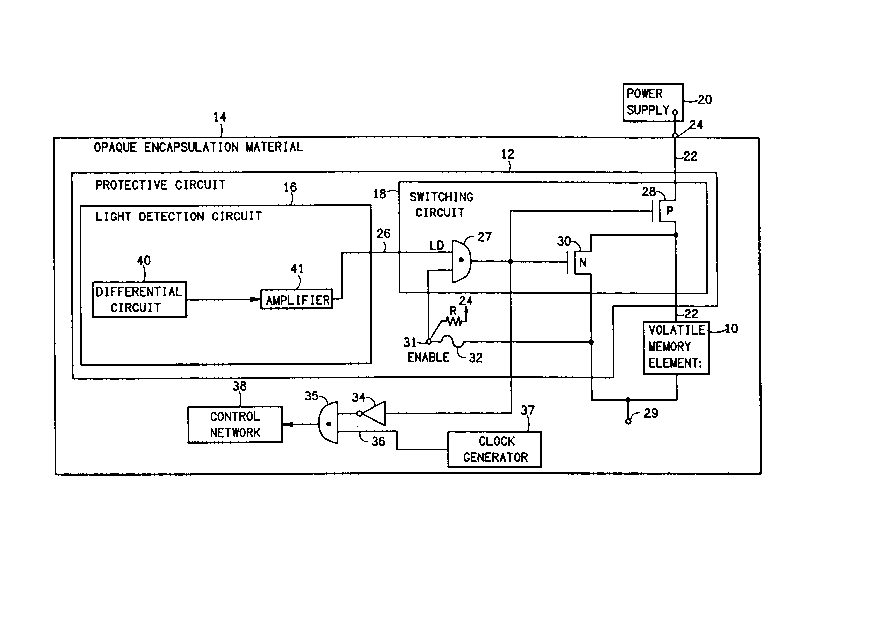
Referring to Flgure 1, a preferred embodiment of the integrated circuil chlp of
the ~-~s~,nl invention includes a secure memory element 10 that stores secret data, a
protective circuit 12 and an opaque layer of material 14 that encapsulates the chlp.
The secure memory elem-~nt 10 iS a volatile memory element that must be coupled to a
po~ver source to retain data stored therein. If power to a volatile memory element ls
interrupted, any data stored therein is el~m~nated rrom the volatile memory element.
F~x~mples of volatile memory elements include, but are not restricted to, a random ac-
cess memory (RAM), and a field programmable loglc arrays wherein the internal logic
operations are to be protected rrom visual inspection attacks Çor such purposes as
reverse engineering.
The proteclive circuit 12 includes a light detection circuit 16 and a switching
circuit 18. The switching circult 18 couples the volatile secure memory element to a
power source 20 by means or conductive elements 22 and a pin contact 24 that ls ex-
posed on the exterior of the chlp. The power source 20 is olT the chip, as shown in
Figure 1. In an alternative embodiment (not shown) the power source is on chip. The
power source 20 for the secure nlemory element 10 is a battery
When the the opaque encapsulatlon materlal 14 is removed rrom the chip, a
light sensitive device in the light detection clrcuit 16 is exposed to light; and such ex-
posure causes a light detection si~nal LD having a HIGH state to be provided on line 26
to the switching circuit 18.
The switching circuit 18 includes an AND gate 27, a PMOS FET 28 and an
NMOS FET 30. The line 26 is coupled via the AND gate 27 to the gate of the PMOS FEr
28 and the gate of the NMOS FET 30. The PMOS FET 28 is connected between the
volatile secure memory element 10 and the power source 20. The volatile secure
memory el~ment 10 is permanently coupled to the substrate of the chip at a pin 29.
The NMOS FET 30 is connected between the drain of PMOS FET 28 and the chip sub-
strate pin 29.
20~2~2
During a LOW signal slate on line 26. the PMOS FET 28 is on and the NMOS
FET 30 ls off so that the volatlle secure memory element 10 is coupled to the power
source 20 by the PMOS FET 28. When light is detected by the light sensitlve element
42 in the protective circuit 12, a HIGH state light detection signal LD ~s provided on line
26 to turn off the PMOS FET 28 and tum on the NMOS FET 30 and thereby disconnectthe volatile secure memory element 10 from the power source 20. When the power
source 20 is removed from the volatlle secure memory element 10, the contents of the
volatile secure memory element 10 discharge to ground within a few seconds and thus
erase or el~m~nate the secret data from the memory 10. The secret data must be erased
quickly enough that it cannot be learned by visual inspection prior to completlon Or
such erasure.
The HIGH state LD signal on line 26 is gated with an ENABLE signal at ter-
minal 31 by the AND gate 27 so that under certain cond~t~on.s the light detection circuit
16 may be essenti~lly disabled. The terminal 31 Is coupled to the power source 20 by a
l~sLstallce R and the pin contacl 24. Thls allows various kinds of arming devices to be
used so that exposure of the llght sensitive device of the light detection circuit 16 to
light cannot impede certain manuracturing operations such as sillcon wafer testing, for
example. Fuses of various kinds which are included in secure integrated circuits for
other security related purposes, as described in United States Letters Patent No.
4,933,898 to Robert C. Gilberg, Paul Moroney, Williarn Allen Shumate and RichardM. Knowles, may be used as such an arrning device.
In the chip of Figure 1, the terrninal 31 is coupled to the substrate pin 29 by
a fuse 32, and thereby coupled to circuit ground so as to prevent the switching circuit
18 from removlng data from the memory element 10 until all manufacturing and testing
operations are completed and the rinal secret data is stored in the memory element 10.
As a final step, the fuse 32 is irTeversibly altered to disconnect the ENABLE terminal 31
from the substrate pin 29 so that the switching circuit 18 is then enabled by the power
source 20. Alternativeh" to the switching circuit 18 thereaiter be~ng continuously en-
abled by the power source 20, the switching circuit 18 can be enabled by an ENABLE
signal being provided to the terminal 31 whenever desired.
2052302
Upon being so enabled, the switching clrcult 18 responds to the llght detec-
tion signal LD produced on line 26 by the light deteclion circuit 16 when the light
cletection circuit is exposed to light by decoupling the volatile secure memory element
10 from the pin contact 24 and thus from the power source 20. to thereby remove
power from the volatile secure memory el~."~.~l 10. Accordingly, should the layer-of
encapsulation material 14 be removed from the chip, power is removed from the volatile
secure memory ~l~ment 10 to thereby cause the secret data to be removed from thevolatile secure memory element, and thus unavailable for visual inspection.
In alternative embo(liment~ (not shown), a s~vitching circuit responds to the
light detection signal LD on line 26 by eliminating secret data from the secure memory
~l~ment 10 by techniques other than by disconnecting the po~ver source rrom the
memory elemlont Such other techniques include erasing the secret data from the
secure memory element by v.~riting null or bad tnon~en~e) data into the secure memory
element
In embo~liment~ used for p~ tlng inspection of data in a nonvolatile
memory, such as an EEPROM, the light detection signal provided by the light detection
circuit trlggers the provision of an erase signal that causes the contents of the EEPROM
to be erased.
The light detection signal LD on line 26 also can be used to disable other on-
chip fimrt~on~ to thereby further disrupt attempts to pirate proprietary information
from the chlp. For P~mple the light detection signal LD is provided via the AND gate
27 and an inverter 34 to one input of an AND gate 35 to inhiblt clock signals provided
to another input of the AND gate 35 from being provided from a clock generator 37 to a
control llelwulk 38 on the chip.
The light detection circuit 16 includes an llnb~l~nced dif~erential circult 40
and an amplifier 41.
2052302
Referrlng to Figure 2 the differential circult 40 includes a flrst light sensltive
diode 42 a first FET 43 and a second FET 44 connected in series with the flrst FET 43
in one arm of the differential clrcuit and a second dlode 45 a third FET 46 and a ~ourth
FET 47 ronn~te~l in series wlth lhe third FET 46 in an opposlng arm of the differential
circult.
The first light sensltive diode 42 has a characteristlc Or a detectable reverse
current change in response to exposure to light. The second diode 45 has a current
characteristlc that is substantlally the same in the absence of light as that of the first
light s~nsIllve diode 42.
The first FET 43 and the third FET 46 are coupled to circuit ground GND by a
fifth tr~n~etor 48 which has its gate connlortecl to a first bias voltage source V~3~ . The
second FET 44 and the fourth FET 47 are conn~ted to a power source Vs. The gates of
the second FET 44 and the fourth FET 47 are connected to a second bias voltage source
VB2. The gates of the first FET 43 and the third FET 46 are respectively connected to
the first dlode 42 and the second diode 45.
A VOUT terminal is connected to the ~unction of the first FET 43 and the
second FET 44; and a VOUr terrnlnal is connected to the ~unction of the third FET 46
and the fourth FET 47.
A second layer of hlghly opaque material 56 covers all of the differential cir-
cuit 40 except for that portion 58 whlch includes the first light sensitive diode 42. The
layer of hlghly opaque material 56 preferably is highly renective metal and Is of such
compos~t'rln that It cannot be removed from the chlp by the same process as may be
used to remove the encapsulation layer 14 without also ~l~m~ging the remainder of the
chip.
The characteristics of the fkst, second, third and fourth FErs 43. 44. 46, 47
are such that while the layer of encapsulation material 14 covers the chlp so that nel-
205230Z
ther the first diode 42 nor the second dlode 45 are exposed to light, the reverse current
IL2 through the second diode 45 is greater than the reverse current ILI through the iirst
diode 42, whereby the voltage at the output terrnlnal VOUr terminal is HIGH and the
voltage at the VOUr terrninal is LOW.
When the encapsulation material layer 14 is removed without also removing
the hlgh~iy renective layer 56, the diode 42 that ls not covered by the highly renective
layer 56 senses the presence of light impinging upon the exposed portion 58 of the chlp
and the reverse current IL1 through the first diode 42 changes by a sufficiently large
amount to exceed the reverse current IL2 through the second diode 45. The reverse
current IL2 through the second diode 45 does not change when the encapsulation
materiai layer is removed, since the second diode 45 remains covered by the highly
reflective layer 56. The values characteristics of the first, second, third and fourth FErs
43, 44, 46, 47 are such that when the reverse current ILI through the first diode 42
exceeds the reverse current IL2 through the second dlode 45,the voltage at the output
terminai VOUT terrninal becomes LOW and the voltage at the VOUT terrninal becomes
HIGH.
The characteristics Or the first, second, third and fourth FErs 43, 44, 46, 47
are also such that operation of the differential circuit 40 is not arrected by such &ctors
as chip noise, device process mismatching, and thermal excitation, so to avoid a false
detection of light in the absence of the encaps-llation material layer 14 being removed.
The voltage at the output terminal VOUT terminal and the voltage at the VOUr
output terminal may be used directly to provide the HIGH state light detection signal
LD on line 26 or, ii- necessaIy, iurther ~mp~ e~l by the :~mrli~lPr 41.
Referring again to the diLferential circuit 40 shown in Figure 2, bipolar~unc-
tion transistors can be substituted for the first, second, third, ~ourth and flfth FEl`s 43,
44, 46, 47 and 48. Device selection is a matter of choice dictated primarily by the par-
ticular integrated circult technology being utilized. The present inventlon may be
adapted to a wide range of technolog~es.
20~2~02
Also, open-base bipolar PNP tr~n~ctors can be substituted for the first and
second diodes 42, 45 to provide light sensltlve elements in the dirrerential clrcuit 40
shown in Flgure 2. Open-base bipolar PNP transistors are available in many CMOS
processes with the advantage of current gain by transistor action over a simple dlode
reverse current approach. A fur~her n~ten~on of thls concept could include Darl~ngton
conflgured transistors.
Figure 3 illustrates an altemative embo liment of a light detection clrcult 16a
that may be used under circumstances that require very low standby current dralnfrom the power source VS. The embodiment of Figure 2 requires a contlnuous supply of
current into the differential ampliriers from the power source Vs~
The light detection circuit 16a of Figure 3 includes a first light sensitive dlode
90, a second diode 92, a third diode 94, a capacitance 96, a flrst NMOS FEI` 98, a
second PMOS FEI` 100 and an NMOS FEI 102. The rirst and second diodes 90, 92 areco....f~led in series between a power source Vs and substrate ground GND. The gate of
the first FEr 98 is connected to the ~unction of the flrst and second diodes. The flrst
FEI' 98 is cormected in series with the third diode 94 between the power source Vs and
substrate ground GND. The capacit~nce 96 is connected between the gate of the first
FEr 98 and substrate ground GND. The second PMOS FEI- 100 and the NMOS FEr
102 are conn~cte~l in series between the power source Vs and substrate ground GND.
The gates of both the second PMOS FEr 100 and the NMOS FET 102 are connected to
the ~lmction 103 of the first NMOS FEr 98 and the third dlode 94. Line 26, on which
the light detection signal LD is provided, is connected to the junction between the
second PMOS FET 100 and the NMOS FET 102.
A second layer of highly opaque material 104 covers all of the light detection
circuit 16a except for that portions 105 which includes the first light sensitive diode 90.
The layer of highly opaque materlal 104 preferably is highly reflectlve metal, and is of
such composition that it cannot be removed from the chlp by the same process as may
be used to remove the encapsulation layer 14 without also d~m~g~ng the remainder of
the chip.
g
- 2~5~2
Operation of the light detection circult 16a is based upon the light induced
reverse current IL1 of the first diode 90 becomine of greater magnitude than the reverse
current IL2 of the second dlode 92 to thereby provide a charging current Il,3 to the gate
of the first NMOS FEI` 98. which will turn on the first NMOS FEr 98 as the voltage
across the capac~tance 96 becomes greater than the threshold voltage required to turn
on the first NMOS FEI` 98.
'Ihe respective characteristics of the first and second light sensltive diodes 90,
92 are such that in the absence of light the reverse current IL1 of the first diode 90 is
less than the reverse current IL2 of the second diode 92, and such that in the presence
of 'iight the reverse current ILI of the first diode 90 is greater than the light induced
reverse current IL2 of the second diode 92. Thus, in the ~bsence of light the voltage
across the cap~it~nce 96 is not charged by the current IL3 and remains less than the
threshold voltage of the first NMOS FEr 98. Accordingly the first NMOS FET 98
remains turned off and the voltage at the ~unction 103 is HIGH due to reverse current
through the FEI` 94 so that the second PMOS FEI` 100 is turned off and the NMOS FEI'
102 is turned on to thereby provide a LOW state signal on line 26.
When the encapsulation material layer 14 is removed without also removing
the highly reflective layer 104, the 'iight in~ ced reverse current IL1 of the hrst dlode 90
becomes greater than the reverse current IL2 of the second dlode 92 to thereby provide
a charging current IL3 to the gate of the first NMOS FEI` 98, which turns on the first
NMOS FEI 98. When the hrst NMOS FEr 98 is turned on the voltage at the ~unction
103 becomes LOW so that the second PMOS FEr 100 is turned on and the NMOS FET
102 is turned offto thereby provlde a HIGH state light detecl~on signal on line 26.
The characteristics of the hrst, second and third diodes 90. 92, 94 and of the
first NMOS FEI' 98 are such that operation of the light detection circuit 16 is not af-
fected by such factors as chlp noise, device process mismatching, and thermal excita-
tion, so to avoid a false detection of light in the ~hsence of the encapsulation matefial
layer 14 being removed.
-10-
2~523Q2
Referrlng to Figure 4, another preferred embodiment Or the light detection cir-
cult 16b includes a first open base bipolar PNP transistor 110 as a light sensltive
devlce, a second open base bipolar PNP tr~n~'stor 112, a first PMOS FET 114, a second
PMOS FET 116 and an ~mplifler 118. The first l~ 's(or 110 and the first PMOS FET114 are connected in series between a power source Vs and substrate ground GND in
one arm of an llnb~l~nre~l differential circuit. The second translstor 112 and the
second PMOS FET 116 are connected in series ~eln~n the power source Vs and sub-
strate ground GND in an opposing arm of the llnb~l~nrecl diiferential clrcuit. The
l~s~ecl~, gates of both FETs 114, 116 are connected to the emltter of the first tran-
sistor 110 at the ~unction of the first transistor 110 and the first PMOS FET 114. The
Input of the amplifler 118 is connected to the emitter of the second translstor 112 at the
~unction of the second transistor 112 and the second PMOS FET 116. Line 26, uponwhich the light detection signal LD is provided, is connected to the output of the
~mpl~fler 118.
A second layer of hlghly opaque material 120 covers all of the light detection
circuit 16b except for a portion 122 which includes the first light sensitive transistor
110. The layer of high-iy opaque material 104 preferably is highly reflective metal, and
is of such composition that it carmot be removed from the chip by the same process as
may be used to remove the encapsulation layer 14 without also fl~m~gjrlg the
rom~ln-ler of the chip.
The operation of the light detection circuit 16b of Figure 4 is essentially digi-
tal and depends on the second PMOS FET 116 and the second transistor 112 adjustlng
their terminal voltages in an attempt to match their currents. In the dark both of the
transistors 110, 112 operate with very small ~unction reverse currents. Exposure to
light causes the light sensitive transistor 110 to operate with a current ILI that is
severa-i orders of m~gnitllde larger than the regular Junction reverse current IL2in the
second transistor 112. These n~smatched currents ILI and IL2 are then converted into
a differential voltage at the emitter of the second transistor 112 that is amplified by the
amplifier 118 to provide the signal on line 26.
`~- 2052302
The respective characteristics of the flrst and second PMOS FETs 114, 116
are such that the reverse current Il l of the transistor 110 is divided by a factor or ten to
provide a current IL2 that flows through the second transistor 112.
In the ahsence of light the resultant current '~.2 through the translstor 112 isvery small and voltage at the emltter of the second translstor 112 is pulled low. thereby
providing a LOW state signal on llne 26 at the output of the amplifler 118.
When the encapsulat~on material layer 14 is removed without also removing
the highly reflective layer 120, the light induced reverse current Il l of the first tran-
sistor 110 increases sllm-~n~ly to pull the voltage at the emitter of the second tran-
sistor 112 HIGH and thereby provide a HIGH state light detection signal LD on line 26
at the output of the amplifier 118.
The characteristics of the first and second transistors 110, 112 and of the
first and second PMOS FETs 114-, 116 are such that operation of the light detection
circuit 16b is not afrected by such factors as chip nolse, device process mismatching,
and thenn~l excit~tion, so to avoid a false detection of light in the absence of the encap-
sulation material layer 14 being removed.
Referring to Figure 5, still another preferred embodiment Or the light detectioncircuit 16c includes a first open base bipolar PNP transistor 122 as a light sensitive
device, a second open base bipolar PNP transistor 124, a third open base light sensitive
bipolar PNP transistor 126, a first NMOS FE,T 128, a second NMOS FET 130, a first
PMOS FET 132, a second PMOS FET 134, a third PMOS FET 136, a fourth PMOS FET
138, a fifth PMOS FET 140, a sixth PMOS FET 142 and an amplifier 144. The first
L,~lslslor 122 and the first PMOS FET 132 are connected in series between a power
source Vs and substrate ground GND in one a~n of an unbalanced differential clrcult.
The second transistor 124 and the second PMOS FET 134 are connected in series be-
tween the power source Vs and substrate ground GND in an opposing arm of the un-b~l~nce~l differential clrcuit. The first and second NMOS FETs 128, 130 and the third,
-12-
20~230~
fourth and fifth PMOS FEI`s 136, 138, 140 are interconnected to rorm an analog dir-
ferential comparator. The first NMOS FEI` 128 and the lhird PMOS FEr 136 are con-
nected ln series v~rith the fifth PMOS FEI` 140 between the power source Vs and sub-
strate ground GND. The second NMOS FEI` 130 and the fourth PMOS FEI` 138 are
connPcte-l in series with the fifth PMOS FEI 140 between the power source Vs and sub-
strate ground GND. The third translstor 126 and the sixth PMOS FEr 142 are con-
nected in series between a power source Vs to provlde a blaslng circuit. The respective
gates of the first PMOS FET 132 and the third PMOS FEr 136 both are connected to the
emitter of the first transistor 122. The respective gates of the second PMOS FEI' 134
and the fourth PMOS FEI` 138 both are connected to the emltter of the second tran-
sistor 124. The respective gates of the fifth PMOS FEr 140 and the sixth PMOS FET
142 both are connecled to the emitter of the third translslor 126. The respective gates
of the first NMOS FFr 128 and the second NMOS FEI` 130 both are connected to the~unction 146 between the second NMOS FEr 130 and the fourth PMOS FEr 138. In an
altemative embo~iment (not shown), the first NMOS FET 128 and the second NMOS
FET are connected in a latch conflguration with the gate of the flrst NMOS FET con-
nected to the ~unction 146 and the gate of the second NMOS FET connected to a junc-
tion 148 between the flrst NMOS FEI` 128 and the third PMOS FEI` 136. In both em-
bo(lim~nt~. the input to the amplifier 144 is connected to the~unctlon 148; and line 26,
upon which the light detection signal LD is provided, is connected to the output of the
~mpl~fler 144.
A second layer of highly opaque material 150 covers all of the light detection
circuit 16c except for those porLlons 152 and 154 which respecUvely include the first
light sel slU~, transistor 122 and the third light sensitive translstor 126. The layer of
highly opaque material 150 preferably is highly reflective metal, and is of such composi-
tion that it cannot be removed from the chip by the same process as may be used to
remove the encapsulation layer 14 without also ~l~m~ging the remainder of the chip.
The light detection circuit 16c of F~gure 5 is based upon the operatlon of the
analog differential comparator 128, 130, 136, 138, 140. In the dark the comparator
-13-
20~2302
and lts blasing circuit 126, 142 are dormant to avoid unnecessary drainage of the
power source Vs, which preferably is a battery, The comparator and its biasing circult
126, 142 come alive only in the presence of light.
When the encapsulalion material layer 14 is removed without also removing
the highly reflective layer 150, the light induced reverse current ILI oi the first tran-
sistor 122 becomes much larger than the reverse current IL2 of the second transistor
124, which is covered by the layer 150 and remains in the dark. The respective cur-
rents I~,l and IL2 through the first translstor 122 and the second transistor 124 are con-
verted into a differentiai voltage between the respective emitters Or the i~rst translstor
122 and the second transistor 124. This differential voltage is compared by the com-
parator 128, 130, lS6, 138, 140, which responds by prwidlng a light detection signal at
the ~mction 148 to the input of the ~mpl~fler 144. The ~mplifi~r 144 ilmplifles the sig-
nal at the ~unctlon 148 to provide a HIGH state light detection signal LD on line 26.
-14-