Note : Les descriptions sont présentées dans la langue officielle dans laquelle elles ont été soumises.
FIELD OF THE INVENTIONS
The present invention .relates to a simplified eleckronic switch suitable .for
modulating the current supplied to an inductive load.
BACKGROUND
1~
Electronic switches for regulating the current supplied to inductive loads are
well known electronic devices. In the case of electromagnetic bearings the
electronic
switch is connected to the coil of the electromagnet. In operation the
electronic-____._.._
switch regulates the amount of current supplied to the coil of the
electromagnet in
response to a control signal. The force delivered by the magnetic bearing is
related to
the amount of current supplied to the coil of the electromagnet. By providing
an
electronic switch capable of modulating the current supplied to the coil of
the
electromagnet, it is possible to modulate the force delivered by the magnetic
bearing.
2 0 Such magnetic bearings are well known and are described in further detain
in, for
example United States Patent No~500142/~- ~' ~ 1 ~' c ' 2 ~~~~ H°zk
E~~,~l
~,____--- ':> °l /o U
P)b(~ 35/la
Electronic switches are typically of an "H-Bridge" design. The "H-Bridge"
design consists of two semiconductor switches and two rectifying dements
arranged to
form an "H" shape. The semiconductor switches are commonly of the N-channel
Field Effect Transistor (FET) type. A FET has three terminals commonly Galled
the
drain terminal, the source terminal and the gate terminal. When the FET is
turned
on, current flows from the source terminal to the drain terminal. To turn the
FET on,
a control signal at a voltage higher than the voltage at the source terminal
must 'be
applied to the gate terminal. When the switch is connected to an inductive
load in the
"H-Bridge" arrangement, the source voltage applied to one of the semiconductor
-2-
~~~~~fl
switches varies as the voltage across the inductive load varies. The gate
control
signal, whose reference is the source of the FET must therefore swing with the
load
voltage. This swing may be hundreds of volts in some applications. Commonly,
an
isolation scheme is used and this entails complicated and expensive circuitry.
In cases
where very fast switching is necessary, additional subtle problems increase
the design
and manufacturing costs. This extra circuit adds to the complexity and cost of
the
to
H-Bridge switch. Although conventional H-Bridge switches are suitable for
certain
applications, the complexity of the switch and the number of expensive
electronic
components comprising the electronic switch results in an unacceptably high
cost for
many applications.
Furthermore, because only one rectifying element means and one
semiconductor switch means are preferably employed, the preferred electronic
switching means of this invention has a lower power loss than that of a
conventional
H-bridge.
It is, therefore, the object of the present invention to provide a simplified
electronic switch arrangement suitable for use with inductive loads.
SUMMARY OF THE INVENTION
Accordingly there is provided an electronic switch suitable for modulating the
current supplied to an inductive load comprising;
(1) a semiconductor switch means;
(2) a rectifying element means;
-3-
~.
(3) an inductive load that contains a first inductive load section and a
second
inductive load section;
(4) an intermediate connection between said first inductive load section and
said
second inductive load section; and
(5) a first power supply terminal and a second power supply terminal wherein;
(a) said semiconductor switch means is connected between said first power
supply terminal and said first inductive load section,
(b) said rectifying element means is connected between said first power
supply terminal and said second inductive load section,
(c) said first inductive load section is connected to said semiconductor
switch means and to said second power supply terminal, between said
semiconductor switch means and said second power supply terminal,
2 0 (d) said second inductive load section is connected to said rectifying
element means and to said second power supply terminal, between said
rectifying element means and said second power supply terminal,
(e) said first inductive load section and said second inductive load section
are connected to said intermediate connection such that the polarity of
said first inductive load section is the opposite of the polarity of said
second inductive load section at said intermediate connection.
Preferably the semiconductor switch means is a Field Effect Transistor,
therefore, minimizing the losses inherent to semiconductor switches. As a
further
preference the rectifying element means is a Diode.
-4-
DETAILED DESCRIPTION
The embodiment of the present invention will now be described by way of
example only with reference to the accompanying drawings in which:
Figure 1 is a schematic diagram of a conventional "H-Bridge" switch and,
Figure 2 is a schematic diagram of the simplified electronic switch
arrangement according to this invention, and
Figure 3 is a schematic diagram of an alternate embodiment of the simplified
electronic switch according to this invention.
Referring to Figure 1, a brief description of the "H-Bridge" switch serves to
describe a typical arrangement and operation of the conventional electronic
switch
when connected to an inductive load. Switch 1 is comprised of two electronic
switch
means shown as Field Effect Transistors (FETs) 2 and 3, and two rectifying
element
means shown as Diodes 4 and 5 and a capacitor 6. The drain terminal of FET 2
is
connected to high potential terminal 8 of a direct current power supply such
as a
battery (not shown). Diode 5 has its cathode connected to the source terminal
of FET
2. The anode of Diode 5 is connected to the low potential terminal 9 of the
power
supply. Diode 5 and FET 2 defines the first FET, Diode series branch.
Similarly,
Diode 4 and FET 3 are connected in series, however in this case, the anode of
Diode
4 is connected to the high potential terminal of the power supply and the
source
terminal of FET 3 is connected to the low potential terminal of the power
supply. A
further connection between the drain of FET 3 and the cathode of Diode 4
completes
the second FET, Diode series branch. One end of inductive load 7 is connected
to the
first FET, Diode series branch between Diode 5 and FET 2. The second end of
the
-5-
~~.o A~
inductive load is connected to the second FET, Diode series branch between FET
3
and Diode 4.
During operation, the simultaneous application of gate signals to the gate
terminals of FETs 2 and 3 causes each FET to begin conducting, thereby
connecting
inductive load 7 across the terminals of the power supply. A current begins to
flow
through the load in the direction indicated by arrow 10 and increases with
time
according to E = L dI , wherein E is equal to the power supply voltage, L is
dT
inductance and c~I is the derivative of I (inductance) with respect to T
(time).
dT
Once the gating signals are removed from FETs 2 and 3, current flow between
the terminals of the power supply through the inductive load ceases. A
potential with
reversed polarity appears across inductive load 7. This voltage causes Diodes
4 and ~
to become forward biased and begin conducting current out of the inductor.
Current exiting from the load through the Diodes charges capacitor 6 which is
connected across the terminals of the power supply. When gating signals are
subsequently applied to FETs 2 and 3, energy stored in the capacitor during
discharging of the inductive load is transferred back into the inductive load
through
FETs 2 and 3.
If, during operation, the length of time that the gating signals are applied
to the
FETs equals the length of time that signals are not applied to the gate
terminals of the
FETs, the electronic switch is said to have a duty cycle of 50% . In this
situation the
average current level in the inductor remains constant. If the gating signals
are
applied to the gate terminals of the FETs for more than half the time the
electronic
_6_
~C'~~r.-~~
.a...a~ ~
switch has a duty cycle of more than Sa%. If the duty cycle is more than 50%,
the
inductor is connected across the terminals of the power supply more than half
the
time. The result is the inductor is being charged for a longer time then it is
being
discharged and the average current through the inductor increases. The reverse
is true
when the duty cycle is less than 50%. The electronic switches conduct for less
than
half the time, and therefore, inductor discharges for a longer time than it
charges
resulting in a decrease in the average current through the inductor.
For a FET to conduct current between its source and drain terminals, the gate
signal must be at a higher voltage then the source terminal voltage. In the H-
Bridge
electronic switch shawn on Figure l, the voltage appearing at the source
terminal of
FET 2 varies due to the charging and discharging of inductive load 7. To
ensure that
FET 2 does not turn off prematurely, due to the source voltage being greater
than the
2o gate voltage, a level shift circuit is commonly used. The level shaft
circuit adds
complexity to the design and increases the cost of the switch. Such level
shift circuits
are well known and are described in .further detail in, for example, the
technical
paper, Power Drives Linking Brains to Braun published in the October 13, 1988
edition of Electronic Design Magazine.
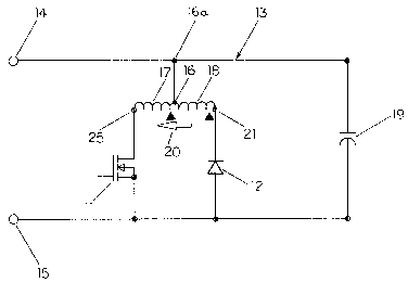
Turning now to the present invention shown on Figure 2, switch 13 contains
one semiconductor switch means shown here as FET 11 and one rectifying element
means shown here as Diode 12. The inductive load connected to the electronic
switch
is comprised of inductive load section 17 and inductive load section 18.
Inductive
sections 17 and 18 have a common connection (connection 16) to the high
potential
terminal 14 of a direct current power supply (not shown). The positive end of
the
_7_
10
windings of inductive sections 17 and 18 are indicated on Figure 2 by
triangles.
Thus, the polarity of the two inductive load sections 17 and 18 must be the
opposite
of one another at intermediate connection 16a. Stated alternatively, the
polarity of the
inductive load sections 17 and 18 is the same at the points indicated by the
triangles of
Figure 2. (As an aside, it should be noted that the inductive load sections 17
and 18
may, in an alternate embodiment, be physically separate from one another. In
this
alternate embodiment, each of inductive load sections 17 and 18 may be
connected by
separate connecting wires to intermediate connection 16a). Between the low
potential
terminal of the power supply 15 and the high potential terminal of the power
supply
14 capacitor 19 is connected. The source terminal of FET 11 is connected to
the low
potential terminal 15 of the power supply. The drain terminal of FET 11 is
connected
to end terminal 25 of inductive load section 17. The anode of Diode 12 is
connected
to the low potential terminal 15 of the power supply and the cathode of Diode
12 is
connected to end terminal 21 of inductive load section 18.
During operation of the electronic switch, a gating signal is applied to the
gate
terminal of FET 11. This causes the FET to begin conducting and results in
inductive
load section 17 being connected across terminals 14 and 15 of the power
supply. A
current begins to flow through inductive load section 17 in the direction
indicated by
arrow 2~. The current through inductive load suction 17 increases according to
the
previously described equation:
E = L _dI
dT
wherein E is equal to the power supply voltage, ~ is equal to the current and
L, equals
_g_
ZO
the inductance of inductive load section 17.
When the gating signal is removed from FET 11, current flow between the
terminals of the power supply through inductive load section 17 ceases. Since
inductive load suctions 17 and 18 are part of one inductive load, the two
sections are
magnetically coupled. The opening of the current path through inductive load
section
17 causes the polarity across both inductive load sections 17 and 18 to
reverse. With
the reversed polarity of inductive load section 18, Diode 12 becomes forward
biased
and allows the charge stored in the inductive load to discharge into capacitor
19.
When a subsequent gating signal is applied to FET 11, energy stored in the
capacitor
during discharging of the inductive :load section 18 is transferred into
inductive load
section 17.
The average current level in the inductive .load comprised of inductor
sections
17 and 18 is controlled in the same manner as with the conventional H-Bridge
switch
previously described. A gate signal duty cycle of 50% results in a steady
average
current through the inductive load. A duty cycle of more this 50% allows the
inductive load more time to charge then to discharge and results in an
increasing
average current value through the inductive load. A duty cycle of less than
50%
allows for more discharging time than charging time and the average current
through
the inductive load decreases.
Figure 3 shows an alternate embodiment of the electronic switch. In this
embodiment, the semiconductor switch means is comprised of a .plurality of
FETs 22
and the .rectifying element means is comprised of a plurality of Diodes 23. If
a single
FET is not capable of conducting the large currents required, a plurality of
FETs may
-9-
~~~ d~~fl
l0
be arranged in parallel. The gating signal would be applied simultaneously to
the gate
terminal of all the FE'fs. The current charging the inductive .load section
would be
divided amongst the FETs.
Similarly, if a single rectifying element was unable to carry the largo
currents
flowing out of the inductive load, a plurality of Diodes may be arranged in
parallel.
The current flow through each Diode would then be reduced.
When used to regulate the current through the winding of an electromagnetic
bearing, inductive load sectors 17 and l~ are formed as the coil of the
electromagnet.
Between the ends of the coil, terminal 16a is provided to form an intermediate
connection between the power supply terminal and the coil. The intermediate
connection formed by terminal 16 may be constructed by various methods. The
coil
for the electromagnet may be first wound and then a separate wire may be
soldered on
2 0 to one of the turns of wire forming the coil. An alternative method of
forming the
inductive load sections would be to wind two separate coils from wire and then
c~nnect one end of each coil to the same terminal of the power supply.
Although the present switch has been described as incorporating FETs, it
should be apparent to those skilled in the art that other semiconductor
switches such
as bipolar junction transistors and the like may be used in place of the FETs
to form
the semiconductar switch means. Similarly the present switch has been
described as
~0
incorporating a Diodes as the rectifying elements forming the required
rectifying
element means. It should be apparent that an alternative to Diodes may be used
to
form the rectifying element means. An alternative to the Diode could be, for
example
a transistor switch arrangement. When the transistor switch arrangement is
used in
-10-
place of the Diodes, an appropriate gating signal would be applied to the
transistor
switch to allow current to flow between inductive load section 18 and
capacitor 19,
and therefore allow the discharge of inductive load section 18.
It should further be apparent to those skilled in the art that modification
and
~0
variations may be made to the present invention without departing from the
scope of
the present invention as defined by the appended claims.
-11-