Note : Les descriptions sont présentées dans la langue officielle dans laquelle elles ont été soumises.
8 i3
INTERCONNECT PACKAGE FOR CIRCUITRY CGMPONENTS
llechnical Fie~d of the Invention
~ his invention relates in general to the packaging of
circuitry components, and in particular to making
interconnections with contact pads of circuitry componants
s,ueh as integrated circuit chips.
Backqround of the Invention
Integrated circuit chips and other circuitry
componants can be coupled to each other and to other
circuits in co~pact modules, units and packages. For
example, ~everal monolithic microwave integrated circ~its
(MMIC's) in chip form can be packaged to provida a unit
capable of operating at microwave and millimeter wave
frequencies. Advancements in GaAs MMIC's, and in
parti~ular, those which operate~ in the millimeter bands,
have made it especially critic:al that connections with
such chips, particularly RF connections, be of the highest
quality. That is, interconnections must be made
con~i~tently such that they provide good impedance match
betwe~n the ~IC and the means of transmission, and the
connections the~qelves must be reliable.
Each MMIC chip may contain several microwave or
millimeter wave circuits such as amplifier, converter or
oscillator circuits dep~ndin~ on the function and level of
integration. For interfacing both DC and RF signals and
currents a MMIC chip has contact pads on one surface,
~5~89
typically around the perimeter of the top surface, which
are connected by interna:L conducting lines to various
portions of the actual circuits wikhin the chip. In the
j case of RF connections between circuits within a chip,
¦ 5 either microstrip or coplanar waveguides are used to form
I wav~guide transmission lines. Chip that use internal
microstrip transmission lines typically have a conducting
ground plane on the bottom surface of the chip in opposing
relation to the transmission lines.
Existing MMIC package~ typic:ally utilize a chip
carri~r, sometimes called a mot~erboard, designed to
support one or more M~IC's. The chip carrier has a
conducting ground plane on one surface and thin ~ilm
metallization patterns disposed on the opposing surface
providing DC and RF interconnection~ among the MMICIs and
betw~en the MMIC I 5 and package input/output terminals.
Ths RF interconnects serve as waveguide transmission lines
employing such techniques as microstrip or coplanar
fabrication.
In such existing MMxc packag~s, MMIC chips are
~ount~d on the chip carrier, typically in recesses in the
carrier surface, and interconnections betw~en contact pads
on the chip urface and intexconnect metallizations on the
chip carrier are made by bonding wires or ribbons. In
so~e existing ~IC package~, longer interconnec~s are made
by mini~tur~ coaxial cable. In another pac~aging method~
known as waf~le line, the chip carrier i made of metal
having a waffle shaped surface ~two-dimensional grooves
20~89
cut into metal). This metal surface acts as a ground
plane; flat areas are created in locations where chips and
other circuit components are to be mounted. DC and RF
interconn~ctions are made by bonding insulated wire to
chip contact pads. The wires carrying RF signals are
pressed into and routed through the waf~le line grooves to
p~o~ide shielding similar to the outer conductor of a
coaxial cable.
Packages for chips operating at lower frequencies or
DC (digital chips, for example) can utilize interconnect
methods similar to those employed with M~IC chips but may
not r~quire the chip carrier to have a ground plane
surface when waveguide tr~nsmission is not employed.
In all o~ the exi~ting interconn~ction methods
discussed, wire, ribbon or cabl.e must be bonded to chip
contact pads, a process in whic,h each connection must be
made either directly by hand or indirectly by an operator
guiding a bonding machine. As can be appreciated,
manually making such interconnections is labor intensive
and time consuming resulting in higher production costs.
Furth~r~ore, because ~f the extremely small dimensions
involv~d~ repeatability of reliable interconnections is
dif~icult to achieve le.ading to inconsistent and less than
optimu~ i~pedance ma~ched interconnects and thus to
performance variations between otherwise identical
packag~. An additional disadvantage of exi~ting
packaging techniques i:; that the chip carrier only
provide~ one level (the carrier sur~ace) for DC and R~
8 9
interconnection networks and for mounting peripheral
circuit components such as chip capacitors. If crossovers
of DC and/or RF interconnections ara re~uired, then extra
wire bonding must be used.
Conseguently, a need has arisen for more consistent
and le~ labor intensive packaging techniques for
circuitry compon~nts to increase repeatability, to provide
more than one circuit lsvel for interconnections and
placement of peripheral component , and to decrease the
production C08t 0~ functional modules.
In accordance with the present invention, a packaging
techniqu~ for circuitry components, including intagrated
cixcuit chips, i~ provided which increa~es the
repeata~ility o~ reliable interconnections, decreases the
production costs, and provides more than one level for
interconnections and peripheral circuit components. All
connections to and from a circuitry component are made
simultaneously in a sinqle proressing step rather than
r~lying on individually hand solder~d DC and RF
conn~ction~
In particular, the present invention provides a novel
package ~or at least one circuitry component which has one
or ~ore interconnect contact pad(~) on a top sur~ace. Th~
packag~ enables the circuitry co~ponant to be
interconnected with other circuitry components and with
circuitq external to ~he package. TAe packag~ includes a
0 3 ~
suppoxt member for supporting the circuitry component and
an interconnect member po5itioned above the circuitry
component. The support member can include a carrier
having a recess for the circuitry component~ The
interconnect member has interconnect transmission lines on
at least one surface for the transmission o~ currents
(including signals) to and from the circuitry component
along with means for coupling the contact pads to the
interconnect transmission lines. In the case of an RF
circuitry component, such as a monolithla microwave
integrat~d circuit ~MMIC), RF coupling between the ~MIC
and interconnect transmission lines can be made by direct
electrical contact or can be made indirectly with
el~ctromagnQtic ~oupling. Low frequency and DC circuitry
component& ar~ coupled with direct alectrical connections.
The package of the present invention permits
interconn~ct transmission lines to be pr~nted on either or
both sur~aces of thQ interconnect:membar and, as mentioned
abov~, opposing contact pads can be coupled in a variety
of ways. For ex~mple, when DC interconnQct transmission
lines ar~ print~d cn the bottom surface o~ the
interconnact mem~er (ie, the sur~a~ facing the chip),
cQupling can be accomplished with solder bumps between the
contact pads (wh~ther on the chip or on th2 support
2S mamber). Wh~n DC interconnect transmission lines are
printed on the top surface of the interconnect member (ie,
the surface f~cing away ~rom the chip), coupling can be
accompli~hed with metallized vias throughout the
2~
interconnect member connected at the upper end to the
interconnect tr~nsmission lines and at the lower end to
solder ~umps which, in turn, provide contact with the
con~act pads on the chip or the support member.
5Similarly, when RF interconnect transmission lines
are printed on the bottom surface of the interconnect
me~ber, coupling can he accomplished with solder bumps
hetween the contact pads. In addition, whether RF
interconn~ct transmission lines are prin~ed on the bottom
10surface of the interconn~ct membor or the top, coupling
can bo acco~plish~d electromagnetically.
To make the interconnections, the circuitry
components are positioned with the interconnect member and
simultaneously bonded thereto. The interconnect member,
15with the circuitry components attached, is then placed
over the support member and so;Ldered in place.
In one embodiment of the present invention, adapted
particularly for MMIC chips, the interconnect member is a
diele~ric interconnect substrate positionad on top of the
20MNIC chips. The interconnect substrate has DC and RF
in~rconneGt transmis~ion lines printed on one or both
surfa~es, the RF interconnect lines being dimensioned in
comb~n~tion with a package ground plane on the support
memb~r and a diQl2ctric positioned in between to provide
2Swaveguides (such as microstrip or coplanar waveguides) of
th~ proper impadance for satisfactory circuit performance.
In one variation of the foregoing embodiment, the
support structure has a chip carrier for the MMIC's. It
28~0~9
has a dielectric top surface and a package ground plane
underneath. MMIC chips are placed in one common recess or
in separate recesses in the chip carrier parallel to the
package ground plane such that chip ground planes on the
NMIC's are in substantial planar contack with the package
ground plane. Conductive interconnect lines for both DC
and ~F can be printed on the top ~urface of the chip
carrier with the RF interconnect lines dimensioned to form
microstrip waveguides in conjunction with the package
ground plane and a dielectric material in between. Each
transmi~sion line in the MMIC, on the ~hip carrier and on
the interconnect substrate terminatQs in a contact pad or
terminal. By matching patterns of contact pads on the
interconnect substrate to patterns of contact pads on the
chips, by matching patterns of contact pads on the chip
carrier to patterns of contact pads on the interconnect
substrat~, and by providing coupling between opposing
contact pads, all RF and DC bias path~ inside the chip
pacXage can be completed.
Consequently, the package of tha present invention
provide~ ~ha t~chnical advantag~ that all DC and RF
interconnactions to and from circuitry components can be
mad~ in a ~ingl~ processing step. Similarly, all
interconnection~ between the int~rconnect mamber and the
~uppoxt member can also be made in a single processing
step. A further adv~ntage of the present invention is
that the interconnact memher provides two additional
levels for interconnect networks and for mounting
~?05~0~9
peripheral circuit elements. This enables RF and DC
interconnect lines to be patterned on different levels
thereby allowiny cross-overs. Also, passive circuit
element such as capacitors, inductors or fiiter
structures can be printed as thin ~ilm metallizations
directly on any of the available surfaces.
For a more complete understanding of the present
invention, and the advantages ther~of, reference is now
made to the following descriptions taken in conjunction
with the accompanying drawings, in which:
Figure 1 illustrates one em~odiment o~ the
int~rconnect package of tha pr~sent invention;
Figure 2 illustrates a cross-s~ctional view of the
e~bodiment o~ the interconnect package illustrated in
Figure l;
Figure 3 illustrates a schematic cross-sectional view
of one embodiment o* the present invention in which
opp~sing D~ and RF contact pacls are directly connected
through ~h~ u~e of solder bumps:
F~gure 4 il~ustrates a qche~atic cros~-sectional view
of an al~rnativ~ e~bodiment of the pre~ent invention in
which opposing RF con-act pads ar~ electromagnetically
coupled;
Figure 5 illustrates an exploded view of one
embodiment o~ the presen~: invention; and
Figure 6 illustrates the interconnect package of
B
2~4~89
Figure 5 with all of the components sealed into place.
De~ailedL E~,~s~;~io~
The present invention is best understood by re~erring
to Figures 1 - 6 o~ the drawinqs, like numerals being used
for lik~ ~nd corresponding parts o~ the various drawings.
The present invention provides a p~ckage for a
circuitry component which has interconnect contact pads on
a top surfaae and allows the ~ircuitry component to be
interconnected with other circuitry components and with
10. circuits external to the package. The package includes a
support me~bar ~or supporting the circuitry component and
an interconnect me~ber positioned aboYe th~ circuitry
component. The ~upport member can include a carrier
having a rece~3 for the circuitry compnnent. The
interconnect member has intercon:nect transmi~sion llnes on
at least one surface for the transmiæsion o~ currents
(including signals) to and from the circui~ry component
along with means ~or coupling the contact pads to the
interconn2Ct transmission lines. In the case of an RF
circui~y component, such as a monolithic microwave
int~gr~ted circuit (MMIC), the RF coupling between the
M~IC an~ interconnect transmisGio~ lines can be made by
dir~ct el~ctrical contact or can be made indireotly with
electromagnetic coupling. Low frequency and DC circuitry
co~pon~nts are coupled with direct electrical connections.
Although th~ followin~ describsd embodiments are
partiaularly adapted for monolithic microwave intsgrated
2 ~
circuit (MMIC) chips, it should be understood that other
embodiments, which provide interconnects for other types
of circuitry components, are within the scope of the
present invention.
Figure 1 illustrates one embodiment of an
interconnect package, generally indicated as 10, for MMIC
chips and other oircuitry components having contact pads
on one surface. A support member, or chip carrier, 12 has
a lower portion or ba~e 13, an upper portion or
input/output (I/0) substrate 15 and a ground means, such
as a package ground plane 14, disposed betw~en upper and
low~r portions 13 and 15. I/0 substrat~ 15 has recesses
16 formed therethrough to ~'xpo8e package ground plan~ 14.
M~IC's, such as that indicated by 18, have a chip ground
plane 20 on one surface (the lower surface in the
orientatlon illustrated) and are retained within recesses
16 such that each chip ground plane 20 is in substantial
planar contact with package gre~und plane 14 across the
surface o~ chip ground plane 20. (As will be appre~iated,
such tQrm~ as "upper~, "lowQr", "above" and "b210w~ are
used ssl~ly to facilita~,e reference to the Figures and are
not int~nded to limiu the present invention to any
particular ori~ntation.)
M~IC 18 ha~ contact pads 22 and 23 on the surface
opposite chip ground planQ 20 (~he upper surface) which
arQ coupl~d to various elem~nts of the circuits contained
within MMIC 18~ Some contact pads 22 provide connections
for DC currents and signals while others 23 provide
2~5~ g
connections for RF signals. RF contact pads 23 are
coupled to waveguide transmission lines within MMIC l~
which, with chip ground plane 20 and a dielectric in
betwean (not shown), d~fine microstrip line waveguides for
transmission of the RF signals inside MMIC 18.
Similarly, various input/o~tput interconnects and
terminal~ (hereinafter collectively ref~rred to as "I/O
intercnnnects") 24 and 26 for DC and RF, respactively, are
dispos6d on the top sur~ace of input/output substrate 15.
Together with package ground plane 14, these I/O
intarconnets 24 and 26 provide means by which MMIC l~
within package lO can be couplad to other cir~uits, po~er
supplies and the like external to pacXage 10.
In contrast to existing chip interconne.ct packages~
in which connections to chip contact pads are made
manually by wire or ribbon bonding, tha interconnect
package 10 of the present invent:ion provid~s a system by
which intexconnections ara made via an interconnect member
pl~ced on top of the 5upport membar. In the embodiment
illustra~ed in Figure lt the interconnect member is a
diel~ctric interconne~t substrat~e 28 placed on top of chip
carriQr 12. Similar to the disposition of I~0
interconnects 24 and 2~ on I/0 substrate 15, DC and RF
interconnect transmission lines 30 and 31 are ~isposed on
interconn~ct substrate 28. These interconnect
transmission lines t~rminate at each end in contact pads.
There are ~wo kinds of contact pads, a first se~ of
contact pads that are matched with opposing I/O terminals
205~g
24 and 26 on I/0 substrate 15 of chip carrier 12, and a
second set of contact pads which are matched with opposing
contact pads 22 and 23 on the top surface of chip 18. To
provide satisfactory impedance matching, the first and
second sets of contact pads may have differ~nt shapes or
sizes.
I/0 interconnects 24 and 26 on chip carrier 12 and
interconnect transmission lines and contact pads
(hereina~ter collectively re~erred to as "interconnect
trans~i sion lines") 30 and 31 on interconnect substrate
28 are preferably patterned on their respective substrates
using conventional thin-film photo-lithographic~etching
technique~ although other techniques can also be used.
In the pre~erred embodiment, interconnect
transmission lines 30 and 31 are disposQd on the bottom
surface of int~rconnect substrate 2~, which faces the top
surfaca of chip carrier 12 and MMIC chip 180 Electrical
connections between opposing RF and DC contact pads can be
made by ~older bumps ~not sho~n in Figure 1). Coupling
betwaen oppo8ing RF contact pads can also be made
el~ctromagn~tically, as will be. detailed below.
In anoth~r embodiment, interconnect transmission
lin~ 30 and 31 are disposed on the top sur~ace of
interconnect substrate 28, facing away ~rom chip carrier
12 and NMIC chip 18 (th~ top sur~ace o~ interconnect
substrate 28), and in a yet other embodiment, interconnect
transmission lines 30 and 31 are disposad on both surfaces
of interconnect subs~rate 280 When top surface
2 ~
interconnect transmission lines are used for maXing DC
connections, metallized via hQles are provided through
int~rconnect substrate 28 to contact pads on the bottom
surfac~ of interconnect substrate 28.
In operation, low frequency and DC currents and
signal~ are connected to DC I/O interconnects 2~ of I/O
substrate 15 and flow through sections of DC I/O
interconnects 24 to connections with DC interconnect
transmis~ion lines 30 on int~rconnect substrate 28,
through DC interconnect tran~mission lines 30 t~
connection~ with DC contact pads 22 on M~IIC 1~. Low
frQquency and DC currents and signals are similarly
conveyed betw~en di~fersnt chips.
RF ~ignals coupled to the I/O RF interconnects 26 are
guid~d by waveguides on chip carriQr 12 to RF interconnQct
transmission linQs 31, then by waveguides on interconnect
substrat~ 28 to RF contact pads 23 on NMIC chip 18. RF
signal~ are al80 guided between dif~erent chips by
coupling the RF contact pads on one chip to RF
interconnect transmi~sion lines 31 on substrate 28 and
back to the RF contact pads on other chips.
~referably, RF interconnect trans~ission lines 31
di~posed on substr2te 2l3 are kept short so a~ to direct RF
signal~ to RF I/O interconnects 26 on chip carrier 12 for
most of the signal path. On the other hand, DC
interconnect transmission lines 30 disposed on
interconnect substrate 28 can bs ~reely routed. This
permits ~eparation of RF and DC interconne~t lines on
2~08~
different surfaces o~ interconnect substrate 28, providing
more freadom in the design of interconnect networks and
crossoversO Similarly, separation o~ DC and RF
interc~nnect networks is possible by using both surfaces
of interconnect substrate ~8 and the top surface of I/O
substrat~ 15.
For satisfactory transmission of RF signals, it is
desirabl~ that the space-or gap between chip carrier 12
and intcrconnect su~strate 28 be substantially uniform.
To provide a substantially uniform gap 25 over chip
carrier 12 and recessed MMIC chip 18. I~0 substrate 15 is
of sub~tantially same thickness as the NMIC chips. Gap 25
should be small enough to provide eP~i~ient coupling
either through fiolder bumps or through electromagnetic
coupling, but not so small that t:he dielectric matexial of
interconnect substrate 28 adversely affects the
perfo~mance o~ the MMIC's. To help reduca the e~act of
interc~nnect substrate 28 on the performance of the
MMIC's, the material in intercolmect sub~trate 28 can be
thinn~d or entirely cut out ju~t above M~IC chip 18.
Th~ uniformity o~ the width o~ the gap can be
controlled in various ways, the preferred method bQing
hard ~tops or spacer~ positioned betw~en interconnect
substrate 28 and chip carrier 1~ in places where such
~pacers will no~ interfere wi~h ~he ~unction of the
circuit.
Figure 2 illustrates a cross sectional view of the
embodim~nt of interconnect package 10 shown in Figure 1.
14
2~o~
MMIC 18 is retained in recess lÇ of chip carrier 12 which
includes base 13, I/0 substra~e 15 and package ground
plane 14. Also shown is a lid 36 which, with a seal ring
38, completely encloses and seals MMIC 18 and dielectrio
interconnect substrate 28. DC and RF chip contact pads 22
and 23, DC and RF interconnect trans~ission lines 30 and
31, and DC and RF I/O int~rconnects 24 and 26 are also
present in the e~bodiment of Figure 2 but are not
illustrated. Between cpposing DC and RF contact pads,
solder bumps 40 ar~ shown.
A mor~ detailed illustration of an RF transition ~rom
MMIC chip 18 to interconnect substrate 28 using solder
bumps is ~hown in Figure 3. In operation, RF energy 56
prop~gates in a waveguide in MMIC 18, comprising package
ground plane 14, microstrip transmission lina 52 on the
top sur~ace of chip 18 and an intermediat~ dielectric
mat~rial. Upon r~aching the end of metallization 52 ! or
an RF contact pad, RF energy 56 is guided through solder
bump 40 to RF interconnQct transmi~sion line 31 on the
underside o~ interconnect substrate 28. RF interconnect
tran~mis~i~n linQ 31, in ~onjunt:tion with package ground
plan~ 14 and th~ intermediate dielectric layer, forms
anothar ~icro~trip wave~uide for continued propagation of
RF en~r9y 60 through package 10. It can ~hen be coupled
to othQr ~IC's or ~o an RF I/0 interconnect 26. DC
currents are conductQd w.'.thout waveguides from DC contact
pad~ 22 on chip 1~ tl~rough solder bump ~0 to DC
interconn~ct transmission lines 30 on substrate 28 and to
DC I/O interconnects 24.
Ancther embodiment uses solder bumps only for
connecting opposing DC contact pads and utilizes
electromagnetic coupling ~etween opposing RF contact padsO
As illustrated in Figure 4, RF energy 56 propagates along `;
a waveguide in chip 18, co~prising microstrip line 52,
package ground plane 14 and an intermediate dielectric
~aterial, to a coupling zone 62. There, RF chip contact
pad 23 is patterned for electromagnQtic, i.e.,
contactless, coupling of RF energy to another waveguide,
again compri~ed o~ RF interconnect transmission line 31,
package ground plane 14, and a dielectric in between.
In the embodiment of the electromagne~ic coupling
illustrat~Qd in Figure 4, RF interconnect tran~mission line
31 is p~ttern2d on the hottom sur~ace o~ dielectric
interconnect substrate 28, which faces MMIC 18. In this
embodi~Q~t, an air gap 25 b~tween RF interconnect
transmission line 31 and package ground plane 14 serves as
the dielectric medium through which the RF enQrgy is
propagated within package 10. In an alternative
e~bodimQnt, ~F interconnect transmission line 31 is
patterned on the top surface of di~lectric interconnect
sub~txate 28, facing away from MMIC 18. In this latter
e~bodiment, dielectric interconnect substrate 28 is,
itself~ part of th~ dielectric layer within the waveguide
bounded by RF interconnect transmission line 31 and
package ground plane 14 and through which the RF energy
propagates.
2 ~ 9
Other arrangements of Dc and RF transmission
interconnect lines 30 and 31 a:re possible within the s~ope
of this invention. For ex~ple, RF interconnect
transmission linss 31 can be printed on th~ bottom surface
of dielectric interconnect substrate 28 and be coupled to
RF contact pads 23 and to RF I/o interconnects 26 with
solder bumps in the manner previously described. DC
i.nterconnect transmission lin~s 30 can be printed on the
top surface of dielectric interconnect su~strate 28 and be
connected to DC pads 22 and to DC I/O interconnects 22
with ~etallizQd vias hrough interconnect substrate 28 to
solder bumps between interconnect s~bstrate 28 and chip
18. In another emhodiment, RF interconnect transmission
lines 31 can be printed on the top surfac~ of dielectric
interconnect substrate 28 and ba electromagnetically
coupled to RF contact pad~ 23 and to RF I/O interconnects
26 while DC interconnect tran;smission lines 30 can be
pr.in~ed on th~ bottom surfacQ and ba coupled to D~ contact
pada 22 and to DC I/O interconnects 22 with solder bump~.
In stlll another embodiment, an interconnect network may
require that so~e of RF interconnect transmission lines 31
be printed on one surface of dielectric interconnect
substr~ta 28 and som~ be printed on tha other surface.
Similarly, 50m~ of DC interconne~t transmission lines 30
can ba printed on one surface o~ dielectric interconnect
substrate 28 and some be printed on the othar surface.
These and other alternative embodiments retain the
technic~l advantages of allowing all interconnections to
-
2 ~
be made securely and reliably in a single step, alLo~ing
millimeter wave transmission of RF signals to and from
~MIC 18, and providing more than one interconnect level.
Furthermore, the use of dielectric interconnect
substr~ta 28 provides two additional surfaces on which to
mount discrete circuit elements or to print thin-film
circuit elements. Thus, a complete package can include
interconnect lines and circuit elements on one or more of
the following three surfaces: the top surface o~ I/O
substrate 15 which ~aces interconnect substrate 28; the
botto~ surface of interconnect substrate 28 which ~aces
carrier 12; and the top surface of interconnect substrate
28 which Sac~s away from carrier 12.
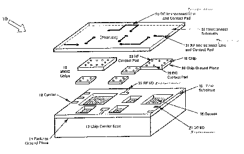
Figure S illustrates an exploded ViQW of the details
of o.n~ e~bodiment of the present invention. As in Figure
1, MMIC's, such as MMIC 18, are r~tainad within recesses
16 of chip carrier 12. The chip ground planas ~not shown)
are in ~ub~tantial pl~nar contact with package ground
plane 14. Dielectric in~ercomlect ~ubstrate 28, having
interconnect transmission lines (not shown), is positioned
Qver the ~MIC~s and carrier 12. Carrier 12 also has
pacXage D~ 2nd RF I/O lnterconnects 24 and 26 to provide
connec~ion~ wi~h other su~h interconnect packages, other
circuits~or external d~vices.
Carrier 12 compris~s upper portion, or I/O substrate,
15 and lowar portion, or base 13. Seal ring 38 is
positioned around carrier 12 to surround diel~ctric
interconnect ~ubstrate 2&. Lid 36 is placed on top of
18
2 ~ 8 9
seal ring 38. The surface of lid 38 which faces
dielectric interconnect substrate 28 can be platad with a
resistive film to dampen cavity modes of the package.
Base 13 may be made of a metal or ~ dielectric providing
strength and good thermal conductivity to conduct heat out
of the package. I/o substrate 15, interconnect substrate
28, seal ring 38, and lid 36 can be made of dielectric
materials which have coe~ficients o~ thermal expansion
which closely match the coefficient of thermal ~xpansion
of the integrated circuit chips retained within carrier
12. When the chips are, for example, GaAs MMIC's, base 13
can be a material such as molybdenum, ~opper-tungsten,
beryllium oxide or silicon; I/0 substrate 15 can be a
material such as alumina (ceramic); interconnect substrate
~5 28 can b~e a material such as alumina or certain glasses;
and seal ring 38 and lid 36 can ~B a material such as
ceramic. It will be appreciatecl that other materials can
also be used.
Referring still to Figure 5, an a~embly procass of
the preferre~ embodiment o~ the present invantion will be
described. The assembly commences with preparation of
chip carriBr 12, M~IC chips, interconnect substrat~ 28,
seal rin~ 38 and lid 360 Chip carrier 12 is assembled by
soldering I/0 substrate 15 with package ground plane 14 ~o
base 13. Interconnect network are patterned on I/0
substrate 15 and interconnect sub~trate 28. Seal ring 38
is secured to chip carrier 12. Solder bumps are plated up
on interconnect transmission lines on interconnect
2 ~ 8 ~
substrate 28 using two solder hierarchies, one that melts
at a higher temperature for the second set of contact pads
(to connect interconnect transmission lines with MMIC
contact pads) and one that melts at a lower temperature
for the first set of contact pads (to connect interconnect
transmission lines with I/O interconnects on carrier 12)~
~MIC chips are aligned one at a time with interconnect
s~bstrate 28 in their respective positions and, using the
higher temperature solder hierarchy, are reflow soldered
to interconnect substrate 28. Once all MMIC chips are
attached, interconnect substrate 28 is itself aligned with
chip carrier 12 and soldered in place using the lower
temperature solder bumps. In the same proces~ chip ground
planes are soldQred to package ground plane 14 inside
recesses~ 16 in chip carrier 12. Finally, l.id 36 is
hermetically sealed on top of seal ring 38 using an even
lower temperature solder hierarchy. Other processes are
available to provide hands-off and cost effective assembly
Or the package of the present invention.
Figure ~ illustrates the package of Figure 5 with all
of th~ co~ponents s~aled in place.
Although the present invention has been described in
detail, it should be understood that various changes,
substitutions and alte:-ations can be made herein without
deporting fro~ the spirit and scope of the invention as
dafined by the appended claims. For example, in another
embodiment, th~ chip carrier of the present invention can
be adapted for other typ~s of circuitry components and
Q ~ 9
integrated circuits and if waveguide transmission is not
required, the package ground means can be omitted.
21