Note : Les descriptions sont présentées dans la langue officielle dans laquelle elles ont été soumises.
.
YO9-gO-081
SINGLE-SCAN TIME DELAY AND INTEGRATION COLOR IMAGING
SYSTEM
Field of the Invention
This invention relates generally to a system which
captures high-resolution color images and in particular,
to a line-sequential color imagihg system which employs
three time delay and integration (TDI) sensors to obtain
a color image of a document.
Background
Electronic color imaging systems generally capture
three distinct spectral components of an lmage, for
example, red, green and blue. Each of these components
is represented by an electrical signal. In many
applications, the separate electrical signals ~re sampled
and digitizèd. If the image is to be stored, the di~ital
samples may be written into a digital memory. The image
may be reproduced by applying the three signals to a
device which combines the colors represented by the three
signals.
Sequential color imaging systems are well known. In
these systems, a single image sensing de~ice sequentially
receives, for example, red, blue and green color
information at a high rate relative to the rate at which
the image is changing. If a document is moving during
the imaging operation, The system must operate at
relatively high fre~uencies since the document must be
resolved into t~ree distinct signals while it is held
momentarily still.
Other existing systems use a single lin~ar or ti~e
dela~ and integration (TDI) imaging device to capture
three separate scans of a document, each taken with a
separate filter in place near the lens. The imaging
device generally resolves lines of picture elaments
(pels) and scans the image incrementally, line by line.
Either the document, the entire system except the
b '~ ~
Y09~90-081 2
document, the imaging device or a system of mirrors may
be moved to provide the scan.
The primary disadvantage of a system of this type i 8
the time required for three scans at a given maximum
output data ra-te. If the document mus-t move while it is
being scanned, it may be necessary to make three passes
through the system to obtain aLl three images. These
passes add to the time required to process the document
and may present ~mdesirable alignment problems.
One method of avoiding multiple passes is to use
three separately packaged imaglng devices together with a
system of spectrally selective beam splitters and
filters. In this system, a different spectral band is
applied to each device. These sy~tems are
disadvantageous because they require expensive optical
components and need precise alignment.
Multiple passes over the image may also be avoided
by placing three imaging devices close together on a
single chip or substrate arranged such that each device
is exposed to light in a different spectral band. This
may be done in several ways. According to a first
method, the light from the illuminated image may be
dispersed so that khe different devices are
simultaneously exposed to different spectral bands. This
method requires a linear filament illuminator and
expensive optical components. Moreover, this method
makes inefficient use of its illuminator and is not
suitable for scanners which move only the imaging device.
A second method employs a uniform illuminator but
places different filters over the different imaging
devices. This method is disadvantageous since it
requires special technology to apply and align the
filters to the devices.
A paper by Yao et al. entitled "A Spatial Image
Separa-tor for Color Scanning" SPIE Vol 809 ~_Scanning
~ f~ 7 ~
Y09-90-081 3
Imagin~ Technology pp 52-54, March 1987, describes a
single-pass TDI color imager which uses a single TDI
array. This system requires relatively complex and,
thus, expensive optical components.
U.S. Patent 4,500,914 to Watanabe et al. relates to
a color imaging array in which red, green and blue sensor
elements are defined by a single charge coupled device
(CCD) imaging array that is tessellated with respective
red, green and blue filter elements.
U.S. Patent No. 4,264,921 to Pennington et al.
relates to a single-pass color imager having three TDI
arrays which each receive different spectral
illumination.
U.S. Patent No. 4,~28,350 to Aughton et al. concerns
an imaging system in which a light beam is
passed through a moving transparency, through a rotating
filter element and onto a single linear imaging device.
The rotating filter element se~uentially passes light in
three distinct spectral components. The light is
converted into electrical signals by the single imaging
device.
Aughton teaches the use of a single linear imaging
device with rapidly changing spectral image components.
The advantages of TDI imaging arrays over linear imagers
are well known: higher effective sensitivity to light and
greater spatial uniformity and fidelity in the captured
image. In a single-pass imager, however, TDI arrays
cannot be substituted for linear arrays in a
straightforward manner. This is because TDI imaging
arrays operate in a pipelined mode, containing an
electronic representation of several image pel lines at
all times. Thus, if known TDI arrays were substituted
for the linear arrays, the three color images would be
mixed togeth~r, preventing color image reproduction from
the electronic output.
7 ~
~09-90-081 4
It is therefore an object of the present invention
to combine the advan-tages of a single-pass color imager
with those of TDI imagers.
Summary of -the Invention
The present invention is embodied in a system and
method for generating multiple spectrum image of a
document in a single scan. 'rhe system includes apparatus
for sequentially applying radiation in N different
spectral distributions to N sensors each of which has at
least one line of pel sensing
elements. The N sensors are arranged so that, as the
document is scanned, the image of each line of pels, in
each of the N spectral distributions, is projected onto
the respective first through Nth sensor elements. Each
of the N sensor elements provides a respective signal
representing the line of pels as if illuminated by a
light of a respectively different one of the N spectral
distributions.
Brief Description of the Drawings
FIGURE 1 is a perspective drawing partly in block
diagram form which illustrates the configuration of key
elements of the imaging system.
., ,
~ FIGURE 2 is a plan drawing which illustrates the
- structure of two optical filters suitable for use in the
imaging system shown in FIGURE 1.
FIGURE 3 is a block diagram which shows how the
imaging system shown in FIGURE 1 may be used.
FIGURE 4 is a plan dr~wing of the sensor element
used in the imaging system shown in FIGURE 1.
;FIGURE 4a is an expanded plan drawing of a portion
of the sensor element shown in FIGURE 4.
S~ r ~ ~ j
YO9-90-081 5
Detailed Description of Exemplary Embodiments of the
Invention
Overview
Although the invention is described in the context
oE a color imaging system in which an image of a scanned
document is developed from three component primary color
images, it is contemplated that it may be used to develop
other types of multiple spectrum images. For example, it
may be desirable to capture both a visible light image
and an infra-red image of an object other than a document
in a single scan or to capture a polychrome image and one
or more monochrome images. One skilled in the art of
designing imaging systems could readily adapt this
invention to perform these functions.
The present invention is described in the contex~ of
a color imaging system suitable or use in an optical
scanner or a color facsimile machine. In these systems,
the document is moved through the machine in incremental
steps. As the document is moved an image of at least a
portion of the document moves across a sensor array.
,
The exemplary imaging system also includes a
rotating disk having three optical filters designed to
produce final captured images corresponding to the red,
green and blue spectral bands defined by the Commission
Internationale de l. Eclairage ~CIE). The rotation of the
disk is synchronized to the motion of the document so
that, as each new line of pels is
imaged onto the sensor array, it is illuminated by a
different spectral component of the light.
The sensor array used in the described embodiments
includes three TDI imaging devices. The basic
operational principles of TDI imaginy devices are
described in U.S. Patent No. 4,264,921 to Pennington et
al., which is hereby incorporated by reference for its
teachings concerning TDI imaging devices. In the
~ 3 ~J
YO9-90-081 6
exemplary embodiments of the invention, each of the three
TDI devices has two masked lines of charge transfer
elements for every unmasked line of pel sensing charge
transfer elements. The shifting of pel signals through
the pel sensing elements and masked elements of the
parallel lines of charge transfer devices is also
synchronized to the motion of the document. This
synchroniz.ation insures tha-t as each new line of pels is
imaged onto the device, the charge packets representing
the previously captured line are shifted to the next
charge transfer elemen-t.
In the exemplary embodiments of the invention each
TDI sensor includes three lines o pel sensing elements
(e.g. lines 412, 414 and 416 of FIGURE 4), separated from
each other by two lines of masked charge transfer
elements (e.g. lines 412 and 412" of FIGURE 4). As the
document is scanned, the charge accumulated in line 412
is shifted into lines 412 , 412" and 414 in se~uence.
The scanning of the document and the shifting of pel
samples through the TDI elements is synchronized so that,
as each line of pel samples is shifted between successive
lines of pel sensing elements (e.g. between lines 412 and
414), the
respective sensing elements are illuminated by the same
line of pels and the same spectral component. Thus, in
the exemplary embodiment of the invention, the charge
accumulated by the TDI device for each spectral component
of each scanned line of pels is integrated over three
exposure intervals.
As the pel samples are shifted out o~ the final line
of pel sensing elements (e.g. 416~ they are applied to a
serial charge transfer shift register (e.g. 418) which
rapidly shifts the entire llne of samples as an analog
signal (e.g. OUT1).
The three TDI sensors are arranged so that, as a
line of pels from the document is applied to each of the
sensors, it is illuminated by a different spectral
Y09-90-081 7
component. Thus, for a given line of pels scanned from
the document, its red spectral component is available at
OUTl, later, its green component is available at OUT2 and
later s-tlll, its blue component is available at OUT3.
The different spectral siyna.ls are available at different
times due to the time required to scan the line of pels
over the sensors 302, 304 and 306.
Each of the sensors 302, 304 and 306 provides
slgnals representing three different spectral components
of any three successive lines of pels. For example, the
sensor 302 may provide the red, green and blue components
for respective successive lines Ll~ L2 and L3 while
sensor 304 provides the green, blue and red components
and sensor 306 provides the blue, red and green
components, respectively. Thus all three color
components of a li.ne of pels are provided as the
three lines are scanned across all three of the sensors.
Detailed Description
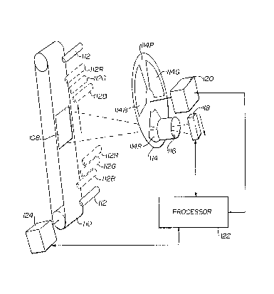
FIGURE 1 is a perspective drawing, partly in block
diagram form, of an optical imaging system which includes
an embodiment of the present invention. In FIGURE 1,
control and data gathering functions performed by a
processor 122 are accomplished via bidirectior.al
connections to the processor, illustrated in block
diagram form.
As shown in FIGURE l, a document 108 is moved
through the imaging system on a belt 110. The motion of
the belt is governed by a motor 124 which is responsive
to control signals provided by the processor 122. In the
exemplary embodiment of the invention, the motor 124 may
be, for example, a stepper motor having a relatively
large number of steps per revolution (e.g. 200). Upon
receiving a signal from the processor 122, the exemplary
motor 124 advances one step, causing an incremental
movement of the belt and thus, the document on the belt.
~ (3~,~
Y09-90-081 8
The rate at which step signals are provided by the
processor 122 determines the .speed of the motor 124.
In a first exemplary embodiment of the invention,
the document is illuminated by two lamps 112 which may
be, for example, conventional quartz halogen lamps.
Light from the illuminated image of the document 108 is
passed through a filter element ll~R of a rotating color
wheel 114 and is projected by a lens system 116 onto an
imaging array 118. The lens
system 116 may be any of a number of conventional lens
systems which do not produce significant distortion in
the image as it is scanned across the imaging array 118.
The exemplary color wheel 114 has three filters
114R, 114G and 114B, which approximate the spectral
distribution shapes required for imaging the respective
red, green and blue CIE color spectra. These filters are
separated by opaque areas 114P. The filters are shown
shaped as sectors of a disk by way of example only. The
color wheel is turned by a motor 120 to expose the imager
118 to different spectral components at different times.
In the exemplary embodiment of the invention, the motor
120 is a stepper motor which is controlled by a pulse
train provided by the processor 122. In the example,
filter wheel 114 is shown in front of the lens 116. As a
matter of design choice~ it may, alternatively, be placed
between the lens 116 and the imager 118.
In a second exemplary embodiment of the invention,
the lamps 112, color wheel 114 and stepper motor 120 are
replaced by three sets of lamps 112R, 112G and 112~ which
emit red, green and blue light, respectively. Each of
these lamps is controlled by the processor 122 to
sequentially illuminate the document 108, and thus the
image of the document on the imaging array 118, with the
different spectral components.
'
Y09-90-081 9
As indicated by the arrows next to the belt 110 and
imaging array 118, as the document moves along the belt
in an upward direction in the FIGURE, the
image of the document moves across the imaging array 118
in a downward direction. In the exemplary embodiment of
the invention, the imaging array contains three sensor
arrays which are composed of charge-coupled devices
(CCD's) operated in time delay and integration (TDI)
mode. The imaging array 118 is described below in
greater detail with reference to FIGURES 4 and 4a.
The TDI sensor arrays on the imaging array 118
capture images oE lines of pels from the document 108 as
photocharge packets. The amount of charge in a packet
represents the brightness of the associated pel. Each
line of pels corresponds to a fine horizontal line of the
document 108. In this embodiment of the invention, the
processor 122 applies a four-phase parallel clock signal
to the TDI arrays on the imaging array 118. In response
to each cycle of the four-phase clock, the charge packets
in one line are shifted downward in the direction of the
image motion. In the exemplary embodiment of the
invention, each line of the image contains 2048 pels and
each pel corresponds to a square on the document having
an area of approximately .00003 square inches.
Correspondingly, each line of sensors in the imaging
array contains 2048 elements.
In this embodiment of the invention, the processor
122 synchronizes the motion of the belt 110 and of the
color wheel 114 to the parallel clock signal applied to
the imaging array. For each cycle of the parallel clock
signal the document on the belt is moved so that the
image of the document advances vertically by one pel
position on the imager 118.
Also, for each pulse of the parallel clock signal the
color wheel rotates to position the next filter between
the lens and the document. The motion of the belt and
the shifting of captured charge in the TDI arrays are
timed to occur when the lens is blocked by one of the
~3~3~.3
YO9-90-0~1 10
opaque regions, 114P of the color wheel 114. As set
forth below, each color component of each line on the
document may be imaged several times as it is scanned
across the image~. The amount of charge accumulated for
each pel position of the line is proportional to the
amount of time that the line is imaged.
When a line of pels has been captured and integrated
~y the TDI sensor, it is shifted out as an.analog signal
in respon~e to a serial clock signal supplied to the
sensor array 118 by the processor 122. This analog
signal is a time se~uence of accumulated charge packets
representing a line of pels in the document.
Since the sensor array 118 includes three TDI
sensors, it is continuously providing three analog
signals. Ih the exemplary embodiment of the invention,
the three sensor arra~s are configured to provideg at any
instant, signals representing three diffe~ent color
spectra. For example, during one cycle of the parallel
clock signal the three sensor arrays may provide red,
green and blue color signal components, respectively,
while in the next parallel clock cycle they may provide
blue, red and green, respectively. These signals are
resolved into separate red, green and blue images by the
processor circuitry described below with reference to
FIGURE 3.
The sensor arrays provide respectively different
color signals at any given time because the number of
masked lines of charge transfer elements between the
bottom row of imaging elements and the serial register
are different for the three arrays. These m~sked lines
delay each output line by one parallel cycle. Thus,
~arying the delay in each array changes the relationship
between the output signals. If, for example, each array
had the same delay, all three arrays would simultaneously
provide output signals for the same color.
~ ~3 ~
YOg-90-081 11
FIGURE 2a is a plan diagram of the color wheel 114
shown in FIGURE 1. This color wheel includes three
filters, one each having a spectral distribution which,
when combined with the spectral content of the lamps and
the spectral response of the imager, corresponds to the
red, green and blue CIE color spectra. These exemplary
filters, however, produce only rough approximations of
the respective CIE spectral bands which are shown in
FIGURE 2c. As shown in this FIGURE, the blue spectral
band z has a peak at ~50 nanometers (nm), the green
spectral band y has a peak at 540 nm and the red spectral
band x has two peaks, one at 600 nm and one at 435 nm.
The peak at 435 nm is at approximately the same
wavelength as the peak of the blue spectral filter. The
red filter 114R in the exemplary color wheel 114 ignores
the effect of the blue peak on spectral transmission.
Accordingly, while this filter may provide an adequate
translation of color from a document to an electronic
image, this translation is not as accurate as it could
be.
Greater accuracy in the transmission spectrum of the
red filter may be achieved by adding a fourth filter to
the color wheel, as shown in FIGURE 2b. In this wheel,
the red filter 114R is replaced by two smaller filters
114RP and 114BP. The filter 114RP has a transmission
spectrum which approximates the peak of the x CIE
tristimulus curve at 600 nm. The transmission spectrum
of the filter 114BP is a reduced-amplitude version of the
z tristimulus curve. This approximates the peak of the x
curve at 435 nm. The inventors have found this to be a
good approximation of the double-peak x transmission
spectrum.
In the exemplary embodiment of the invention, the
red peak filter 114RP is smaller than the red filter 114R
shown in FIGURES 1 and 2a. This filter provides
acceptable performance, however, since the TDI sensors
exhibit greater sensitivity to light at the red end of
the spectrum than to light at the blue end of the
'
2 ~ r~ ~
Y09-90~081 12
spectrum. In operation, the imaging array 118 would be
exposed light from both of the filter elements 114RP and
114BP during a single cycle of the parallel clock signal
PC. The array 118 would only be exposed to light from
one of the filter elements 114G and 114B respectively
during each of the next two successive clock cycles.
Although the wheel 114 is shown as only having one
filter element of each color, it is contemplated that an
alternative wheel may have multiple filter elements of
each color. This would be advantageous since it would
allow the speed of the stepper motor 120 to be reduced,
since all of the filter elements could be inserted
between the document and the imaging array 118 is a
portion of the rotational period of the motor.
As shown in FIGURE 1, the lamps 112, color wheel 114
and stepper motor 120 may be replaced by thrèe sets of
filtered light sources 112R, 112G and 112B which a~e
individually activated by the processor 122 at times
corresponding to the illumination of the image by the
filters in the wheel 114 in the embodiment described
above. In this alternative embodiment, the blue peak of
the x CIE tr~stimulus curve may be approximated by
briefly activating the blue light source during the time
interval in which the red light source is activated.
FIGURE 3 is a block diagram which shows details of
the imaging array 118 and of the components of the
processor 122 which send control signals to, and receive
data from the imaging array 118. As described above, the
imaging array 118 includes three component TDI arrays
302, 304 and 306. These arrays are described below, in
greater detail, with reference to FIGURES 4 and 4a.
.
A clock generator clrcuit 330 provides parallel
clock signals, PC, and serial clock signals, SC, to each
of the component TDI arrays of the imaging array 118. It
is understood that PC and SC each symbolically represent
multiple conductors conveying multiple clock signals to
Y09-90-081 13
the parallel and serial registers of the imaging arrays.
For example, PC may comprise four parallel phases and a
parallel-to-serial interface phase~ while SC may comprise
four serial phases, a set phase and a reset phase. All
serial phases and all parallel phases have respective
common fre~uencies. In this embodiment of the invention,
the signals PC and SC have fre~uencies of appro~imately 4
KHz and 8 MHz, respectively. The exemplary clock
generator circuit 330 also provides clock signals to
stepper motor controllers 334 and 336 which control the
belt stepper motor 124 and color wheel stepper motor 122,
respectively. In addition, the clock generator provides
other clock signals, described below, which are used by
components of the processor 122. By controlling the
frequency and phase of these clock signals, the processor
122 synchronizes the motion of the belt 110, the color
wheel 114 and the shifting of packets through the TDI
sensor arrays as described above.
Each of the component TDI arrays 302, 304 and 306
provides an analog output signal to a respective
analog-to-digital converter (ADC) 308, 310 and 312. Each
analog output signal is generated by serially shifting
2048 charge packets, representing a line of pels, from
the array synchronous with the signal SC.
The ADC s 308, 310 and 312 each receive, from the
clock generator 330, a clock signal having the same
frequency as the signal SC but with a phase determined by
the analog output signal. In response to this signal,
the ADC s 308, 310 and 312 generate digital values
representing the respective analog chargè packets
provided by the imaging arrays 302, 304 and 306,
respectively. Each of the ADC's 302, 304 and 306
provides the digital values that it produces to three
multiplexers 314, 316 and 318. Each digital value is in
the form of eight parallel bits. In this example this
signal is shown as a single pa-th for clarity.
.
Y09-90-081 14
The multiplexers 314, 316 and 318 are all coupled to
receive a two-bit control signal from a modulo~three
counter 320. The clock input signal to the counter 320
is provided by the clock generator 330 and has
substantially the same frequency as the parallel clock
signal ~C. As shown in FIGURE 3, the multiplexer 314 is
configured to pass the signal provided by the ADC s 308,
310 and 312 when the values provided by -the counter 320
are 0, ~ and 2, respectively. For these values, the
multiplexer 316 is configured to pass the values provided
by the respective ADC's 310, 312 and 308, while
multiplexer 318 is configured to pass the values provided
by the ADC s 312, 308 and 310.
In this configuration, the samples provided by each
multiplexer represent a separate color component of the
image. Which color component is passed by which
multiplexer depends on the synchronization of the color
wheel 114 to the clock signal PC. In the exemplary
embodiment of the invention, the color wheel rotates to
expose the sensor array to red~ green and blue light in
succession. Thus, with the proper phasing of the two-bit
control signal, the exemplary multiplexers 314, 31~ and
318 provide red, green and blue sample values,
respectively.
The samples provided by the multiplexers 314, 316
and 318 are applied to respective digital memory arrays
322, 324 and 326. Each of these memories has sufficient
capacity to hold samples representing an entire document.
In the exemplary embodiment of the invention, where the
document 108 may be 11 by 14 inches and where each pel
represents a square on the document having an area of
.00003 square inches and 256 greyscale values, the
exemplary memory arrays each contain more than 5,000,000
bytes (5 MB) of data storage.
The memory arrays 322, 324 and 326 include
conventional dual-port random access memory (RAM)
elements. Data may be stored into these RAMs in response
,
. . ,
Y09-90-081 15
to a first set of address signals, provided ~y address
logic 332, while stored data is independently read from
the arrays in response to a second set of address
signals, provided by application circuitry 328. This
application circuitry may be, for example a conventional
color facsimile transmission system.
Due to the configuration of the imaging array 118,
i red samples representing one line of pels (e.~. Ll)
are provided by the TDI sensor array 302, red samples for
the next two lines on the document (e.g. L2 and L3) are
provided by the sensor arrays 304 and 306, respectively.
Not only are these lines of samples provided by different
senæor elements but, in this embodiment of the invention,
they are delayed, respectively, by 15 and 30 cycles of
the parallel clock signal PC with respect to the line of
samples provided by the sensor element 302.
In addition to the above considerations for
generating address values for successive lines of samples
of a single color, other considerations exist for
generating address values for the different color
components of a single line of samples. Using the line
Ll described above, if the TDI sensor array 302 provides
the red samples for line Ll, the sensor array 304
provides the green samples and sensor 308 provides the
blue samples with respective delays of 1~ and 28 cycles
of the signal PC.
To handle this addressing scheme, the exemplary
address logic 332 is coupled to receive a clock signal,
MC, having substantially the same frequency as the serial
clock signal SC. In addition, the address logic 332
receives the counter value provided by the counter 320 to
the multiplexers 314, 316 and 318. The exemplary logic
circuitry 332 contains three address counters (not
shown), one for each of -the memories 322 9 324 and 326 and
stores three address values (not shown) for e~ch memory.
The address value that is loaded into a particular
YO9-90-081 L6
counter is determined from the signal provided by the
modulo 3 counter 320. ~ll three of the counters in the
address logic 332 are incremented synchronously with the
clock signal MC.
The circuitry shown in FIGURE 4 assumes that the
various sensor arrays, 302, 304 and 306 simultaneously
provide signals representing different spectral
components. If, as set forth above, the sensor arrays
are identical and, so, provide signals representing the
same spect~al components, the memory 322 would be
segmented differently requiring changes in the address
logic 332. One skilled in the art of desighing image
processing circuitry can readily design suitable
circuitry to handle the signals provided by the
alternative sensor arrays.
FIGURE 4 is an expanded plan view of the sensor
array 118 shown in FIGURES 1 and 3. FIGURE 4a is a
further expànsion of a portion of the sensor array 302.
These two FIGURES are used to describe the configuration
and operation of the imaging array 118.
As described above, the imaging array 118 includes
three component TDI sensor arrays, 302, 304 and 306.
Sensor array 302 has three lines of 2048 pel imaging
cells (412, 414 and 41~) which accumulate charge when
exposed to light. The imaging cells in lines 412 and 414
are separated by two lines of masked cells, 412' and
412". These masked cells are not light sensitive and
merely act as two stayes each of 2048 parallel CCD shift
registers, which pass the charge packets from the line
412 to the line 414. There are also two lines of masked
cells between the lines of pel imaging cells 414 and 416
and between the pel imaging cells in the line 416 and a
2048 stage parallel input serial output CCD shift
register 418.
FIGURE 4a is a plan diagram of a portion of the TDI
array 302. The array includes three rows of imaging
YO9-90-081 17
cells, 412, 414 and 416. Each of the rows of imaging
cells is separated from the next row by two rows of
masked cells ~e.g. 412 and 412"). 'rhe parallel clock
signal PC, includes, in this embodiment, four phase
signals which are applied to all of the masked and
unmasked rows of cells. The four-phase clock signal acts
to transfer charge packets, in parallel, from one row of
the TDI array to the next. The exemplary signal PC also
includes à parallel-to-serial transfer phase. The
discussion that follows describes the operation of the
TDI array in terms of time intervals defined by
successi~e cycles of the signal PC.
,
During a first cycle of this signal, the charge
packets Pl, P2 and P3 are accumulated while row 412 is
exposed to, for example, a line, Ll of pels from the
document illuminated by red light (at the same time other
charge packets are being accumulated in rows 414 and 416
by exposure to other lines of the document, also in red
light). These charge packets are transferred to row 412'
to become the packets Pl , P2' and P3 at the start of
the next cycle. During this -time interval, the line of
pels Ll is focused on row 412 and the entire imaging
array is exposed to green light. The amount of charge in
the packets held in row 412 is substantially unchanged
during this cycle because the effect of light on the
masked row of cells of row 412 is negligible.
During the next cycle, the packets Pl , P2 and P3
are transferred from the masked row 412 to the masked
row 412" to become the packets Pl", P2" and P3". During
this interval the pels of line Ll are focused on the row
412" and the imaging array 118 is exposed to blue light.
As with row 412 , the amount of charge in the packets
Pl", P2" and P3" remains substantially constant; there is
no contribution from the blue light.
In the next cycle, the ~ackets Pl", P2" and P3" are
transferred into the imaging cells of row 414, becoming
Pl" , P2"' and P3" . The pels of line Ll are then
l r~
Y09-90-081 18
focused on the row 414 and the array 118 is again
illuminated by red light. During this interval, the
light shining on the imaging cells increases the charge
in packets P1" , P2" and P3" .
During the next two cycles of the signal PC, the
charge packets representing the pels of line L1 are
transferred through the cells 414' and 414". In the next
subse~uent cycle, charge is again accumulated in the
packets while they reside in the imaging cells of row 416
and are exposed to line L1 in red light. These charge
packets are then transferred through the rows 416' and
416" in the next two cycles.
Upon leaving the row 416", at the start of the next
cycle, the accumulated charge packets are transferred, in
parallel, into a parallel input, serial output shift
register 418 by the parallel-to-sèrial phase of the clock
signal PC. During that cycle, these charge packets are
shifted out o the shift register 418 in response to the
8 MHz clock signals, SC. The set and reset phases of the
signal SC aid in the generation of the analog output
signal from the serial register.
It is noted that, at any time, charge packets reside
in all elements of each array so that the opexations
described above are occurring simultaneously throughout
the imaging array.
The structure of the component TDI arrays 304 and
306 is the same as the array 302 except for the number of
rows of masked cells between the last imaging line and
the output shift register. In the array 304j only one
row of masked cells is present bétween the last line of
pel imaging cells, 426 and output shift register 428. In
the TDI array 306, the output shift register 438 is
coupled directly to the las-t line of imaging cells, 436
with no intervening rows of masked cells.
YO9-90-081 19
The number of lines of cells is different for the
different TDI arrays to ens~re that no two arrays will
simultaneously provide samples of the same spectral
component. As described above, all of the TDI arrays are
simultaneously exposed to each of the three spectral
components and all of the arrays are responsive to the
clock signal PC to transfer the accumulated charge
packets in each line to the next successive line. Thus,
if all of the TDI arrays had the same number of lines
then they would all simultaneously provide samples of the
same spectral component at the output ports of their
respective serial shift register stages. In the
configuration shown in FIGURE 4, while the TDI array 302
is providing red spectral samples at its output terminal,
the arrays 304 and 306 are providing green samples and
blue samples, respectively.
The ihdividual TDI arrays 302, 304 and 306 are
arranged on the sensor array 118 so that the distance d
between the first line of ima~ing cells o~ any two
successive arrays is a multiple of the spacing
represented by three lines of.cells (imaging and non-
imaging) plus the spacing represented by one additional
line. As a practical design consideration, it is
desirable that the spacing be large enough to permit
electrical connections to the individual arrays 302, 304
and 306. In the exemplary embodiment, the distance d is
equivalent to 16 line widths (5*3+1). In other
embodiments of the invention where each TDI sensor array
may include, for example, 33 lines of cells (11 imaging
lines and 22 masked lines), a distance d of 52 line
widths may be more appropriate. As an alternative, the
distance d may be equivalent to a multiple of three line
spacings, minus one line spacing. In ~IGURE 4, the
spacing between the arrays is not shown to scala.
This arrangement of the respective TDI sensor arrays
ensures that each line of pels is imaged in each of the
three color spectra, red, green and blue. As set forth
above, the motion of the belt is synchronized to the
2 ~3
Y09-9~-081 20
motion of the color wheel and the parallel clock signal
PC so that for each cycle of the signal PC, the image of
the document is moved vertically down the imager by one
pel position and the color wheel is rotated to expose the
imaging array to a different spectral component. Using
this scheme, each unmasked row of imaging elements is
exposed to the same lines of pels for a given spectral
component. For example, when line 412 is exposed to a
line of pels Ll in red light, lines ~14 and 416 will also
be exposed to the same line of pels in red light
respectively 3 and 6 cycles of the signal PC after line
412 is exposed.
As the image of the document is scanned down the
imaging array 118, if a given line Ll is exposed in red
light on the imaging lines of the TDI array 302, it is
exposed in green light on tha imaging lines of the TDI
array 304 ahd in blue light on the imaging lines of the
TDI array 306. Th~s, every line of pels in the document
is imaged in all three spectral components.
In the exemplary embodiment of the invention, there
are delays of 15 and 30 cycles of the signal PC between
the time that the line of pels in one spectral component
is provided by the TDI array 302 and the times that the
other two spectral components of the line are provided by
the respective TDI arrays 304 and 306. These delays
would increase if each of the TDI arrays used more rows
of cells or if the spacing between successive TDI arrays
were increased.
While the described embodiments of the invention use
TDI sensor arrays, it is noted that linear image sensors
(not shown) may be substituted for the TDI arrays. In
this alternative embodiment, three linear image sensors
would be placed in the same relative positions on the
sensor array 118 as described above. Each succes~ive
pair of linear sensors would have the spacing between
their lines of imaging cells as described above. This
configuration of linear sensors would allow t~le use of a
2 f~ r ~ ~j r
Y09-90-081 21
lower data rate from each sensor than in the imaging
apparatus set forth in thé above referenced Auyhton
patent.
While this invention has been described in terms of
an exemplary embodiment, it is understood that it may be
practiced as outlined above within the scope of the
attached claims.