Note : Les descriptions sont présentées dans la langue officielle dans laquelle elles ont été soumises.
2056Q21
A digital quadrature phase detection circuit
FIFLI) OF ~IE INV~TION
This invention relates to a phase detection circuit
that detects the phase changes of an angle modulated signal
and derives an in-phase component level(I signal) and a
quadrature component level (Q signal) of the input signal
relative to a reference signal.
~ACKGROUND OF THE INVENTION
Quadrature detectors are conventionally used as a
means o~ detecting the phase changes of a high-frequency
signal. An example of this kind of detector is shown in
FIG.2 where an input signal S1 is multiplied by the double-
balanced mixers 21 and 22 using local signals S21 and S22,
respectively. The signals S21 and S22 are generated by a
local oscillator 23, and the phase of local signal S21 is
shifted by a ninety degree phase--shifter 24, so that the
phases of signals S21 and S22 are ninety degrees apart.
The outputs S23 and S24 of mixers 21 and 22 are applied to
low--pass filters 25 and 26, respectively, which remove the
high frequcncy components of signals, S23 and S26 and
produce baseband signals S25 and S26 with phases which are
orthogonal each other. Based on a sampling pulse P, analog-
to~ igital (A/D) converters 27 and 28 convert S25 and S26,
respectively, to digital signals which are then outputted as
detection results or as I and Q signals.
-1- *
20~;~o2 1
The above process can be described by the followin~
mathematical expressions. Let the input signal S1 be
x = 2 Acos(~ ct+ ~ ) (1)
and let the local signals S21 and S22 be respectively
Y21 = cos(~ ct)
Y22 = -sin( ~ ct) ~2)
then the outputs S23 and S24 of mixers 21 and 22 are
respectively given by
23 x Y21 = Acos(2~ ct+ ~ )+ Acos(~ ) (3)
Z24 = x Y22 = -Asin(2~ ct+ ~ )+ Asin(~ ). - (4)
where
~ c : the angular frequency of the carrier of an input
signal S1(radian/sec)
t : time (sec)
~ : the phase of input signal S1(radian).
The values of the I and Q signals whose hi8h frequency
components are removed by the low-pass filters 25 and 26
ar- res~ectively
I = Acos(~ ) Q = Asin( ~ ). - ............ ......... (5)
~-e phase ~ can be derived from the I and Q si~nals
a-cording to the relationship,
~ = tan~l(Q/I). - - (6)
The foregoing describes the principle behind the operation
of a conventional quadrature detector.
The conventional quadrature detector described above
20 5602 1
has several problems as follows;
(1) It is very difficult to accurately implement tlle
ninety de8ree phase-shifter(24 in FIG.2). An error with the
phase-shifter directly results in an error in the phase
S detection.
(2) Since it is difficult to accurately balance the two
mixers 21 and 22, a DC off-set inevita~ly appears in the
baseband signal. This also results in an error in the phase
detection.
10(3) An amplitude deviation appears where an unbalance
occurs between the mixers 21, 22 and the low pass filters
25 and 26. This also causes an error in the phase detection.
To reduce these errors, a considerable amount of
adjusting processes are required. Even if these adjustments
15are successful, the errors caused by fluctuations in the
characteristic values of the devices as caused by
temperature changes or aging cannot be prevented. In
addition, the integration of analog circuits such as
mixers, a ninety de8ree phase-shifter and low pass filters
20is difficult, makin8 reductions in the size of the detector
al~ power consumption difficult.
SUMMARY OF THE INVENTION
An object of the present invention is, therefore, to
provide a pllase detection circuit which easily solves the
problems described above.
205602 1
66446-521
Another ob~ect of the present lnventlon ls to provlde
a phase detectlon clrcuit capable of ellmlnatlng a DC off-set
contalned ln an lnput slgnal by uslng an A/D converter, delay
clrcults, adders and latches.
Yet another ob~ect of the present inventlon is to
provide a phase detection clrcult havlng no analog devlces, such
as a phase-shlfter or mlxer, and thereby ellmlnates phase errors
ascrlbable to these devlces.
A further ob~ect of the present lnventlon ls to
provlde a phase detectlon clrcult lmplemented by dlgltal
clrcults except for an A/D converter and thereby easlly
fabrlcated ln a large scale lntegrated (LSI) clrcuit.
According to one aspect of the lnventlon there ls
provlded a detector clrcult comprlslng:
A/D converter means for convertlng an analog angle-
modulated slgnal lnto a dlgltal slgnal by uslng a clock slgnal;
a plurallty of delay means connected ln serles to the
output of sald A/D converter means, each delaylng an lnput
thereto by one perlod of sald clock slgnal;
a plurallty of welghtlng means for welghtlng sald dlgltal
slgnal and the output of sald plurallty of delay means;
flrst adder means for addlng the welghted dlgltal slgnal
and the welghted outputs of even numbered delay means from sald
A/D converter means;
second adder means for addlng the welghted outputs of odd
numbered delay means from sald A/D converter means; and
flrst and second latchlng means for respectlvely latchlng
~, ,~,
2 0 5 60 2 1
66446-521
the outputs of said flrst and second adder means in
synchronizatlon wlth a latchlng slgnal havlng a perlod _ tlmes
longer than the perlod of sald clock signal to produce in-phase
and quadrature components of sald angle-modulated signal.
Accordlng to another aspect of the invention there is
provided a method of detectlng an analog angle-modulated signal
to produce its in-phase (I) and quadrature (Q) components, sald
method comprising the followlng steps of:
converting said analog angle-modulated slgnal lnto a
digital slgnal in synchronlzatlon with a clock slgnal having a
frequency n tlmes higher than the carrier frequency of said
angle-modulated signal, n belng a positlve integer;
sequentially delaying said digltal signal n tlmes by one
period of said clock signal each;
weighting said digital signal and the 2~-tlme delayed
slgnals wlth a flrst set of predetermlned weighting factors to
produce a first set of welghted signals, P being 1, 2, n/2;
weighting the (2~-1)-time delayed signals to produce a
second set of weighted signals;
adding said first set of weighted signals to produce a
first added signal;
addlng said second set of weighted signals to produce a
second added signal; and
latching said first and second added signals with a
latching slgnal havlng a perlod n tlmes longer than the perlod
of said clock signal to produce said I and Q components,
respectively.
205602 1 66446-521
DBSCRIPTION OF THE DRAWINGS
The above and other ob~ects, features and advantages
of the present lnvention wlll become apparent from the followlng
descrlptlon referrlng to the accompanylng drawlngs, in whlch:
FIG. 1 ls a block dlagram lllustratlng a phase
detectlon clrcult accordlng to an embodlment of the present
lnventlon; and
5a
,~
205602 1
FIG.2 is a block diagram of a conventiollal phase
detection circuit.
DETAILED DESCRIPTION
OF THE PERF~ERED EM~ODIMENT OF THE INVENTION
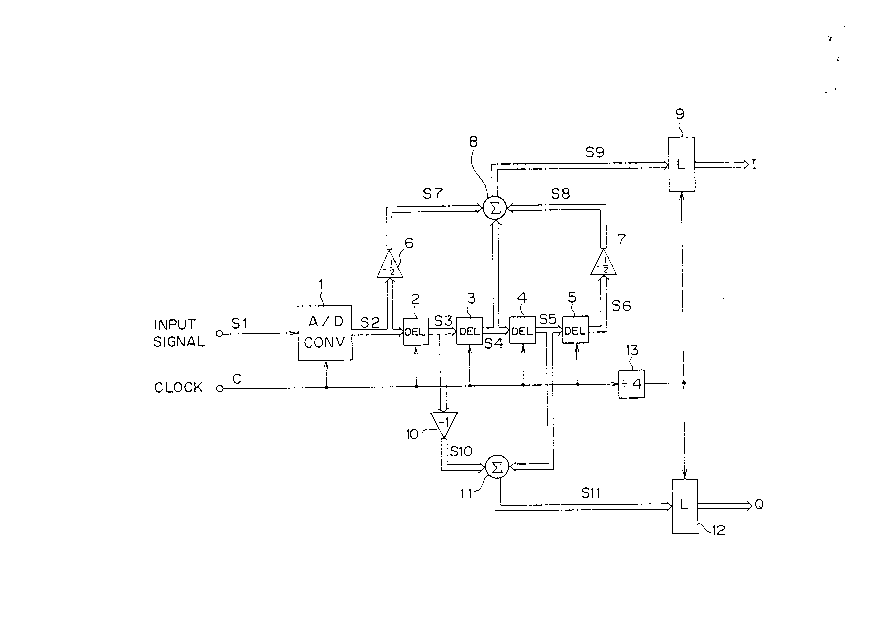
5In FIG.1, an Af~ converter 1 converts an input signal
Sl to a digital signal S2 in synchronizatiOn with a sampling
clock C having a frequency four times higller than the
carrier frequency of signal Sl. The digital signal S2 is
delayed by one sampling cycle of clock C by delay circuits
102, 3, 4 and 5, respectively, whicll output respective delayed
signals S3, S4, S5, and S6. The digital signal S2 is
weighted by a weighting factor of -1/2 at a weighting
circuit 6 to become a signal S7. l~le output S6 of the fourth
delay circuit 5 is weighted by a weighting factor of -1/2 at
15a weighting circuit 7 to become a signal S8. The outputs S7
and S~ in addition to the output S4 of the second delay
circuit 3 are added by a first adder 8, the output of which
(S9) is latched to the first output latching circuit 9 at a
cy-le follr times longer than the sampling clock cycle. ~liS
20latching cycle is obtained by dividing the samplirlg clock C
at a divider 13. The latched signal is outputted as an I
signal(in-phase component level).
In additiorl, a weighting circuit 10 weights the outpul
S3 of the first delay circuit 2 with a weighting factor of -
1 to reverse the polarity of same and thereby to produce an
205602 1
output S10. The output S10 and the output S5 of the third
delay circuit 4 are added by a second adder 11. The output
of second adder 11 is then latched to a second output
latching circuit 12 at the latching cycle provided from
divider- 13. This latched signal is outputted as a Q signal
( quadrature component level ).
The above-described operation can be described by the
following mathematical expressions. Let the input signal S1
be
~ = Acos(~ ct+ ~ )+ v, - ........................... (7)
and let the sampling timing within the A/D converter 1 be
t = nT. -- -- .
where,
n = -{o, - , -2, -1, 0, 1, 2, - , ~ . .............. (9)
T = 2~ /4~)c : the sampling cycle ( with the sampling
frequency 4-times longer than the carrier
frequency) (10)
v = the DC off-set.
According to the above definitions, signals S2, S3, S4,
S5, and S6 are respectively expressed as
S2 = Acos(~ cnT+ ~ )+ v
S3 = Acos(~ c(n-l)T+ ~ )+ v
S4 = Acos(~ c(n-2)T+ ~ )+ v ........... (11)
SS = Acos(~l)c(n-3)T+~ )+v
S6 = Acos(~ c(n-4)Tt- ~ )+ v
205602 1
Here, n = 4m+ k.
Where,
= -co, , -2, -1, 0, 1, 2, , oo
k = 0, 1, 2, 3,
then, the expressions (11) become
S2 = Acos(~ c(4m+ k)T+ ~ )+ v
S3 = Acos(~ c(4m+ k-l)T+ ~ )+ v
S4 = Acos( ~ c(4m+ k-2)T+ ~ )+ v ........... (12)
S5 = Acos( ~ c(4m+ k-3)T+ ~ )+ v
S6 = Acos(~ c(4m+ k-4)T+ ~ )+ v.
Substituting the e~ressions(10) into the expressions(12)
and allowing the latching timing in the OUtpllt circuit 9 an~l
12 to at the time when k=2, then each delay signal can be
expressed as
S2 = Acos(2~ m+ ~ + ~ )+ v
S3 = Acos(2~ m+ ~ /2+ ~ )+ v
S4 = Acos(2~ m~ )+ v (13)
S5 = Acos(2~ m-~ /2+ ~ )+ v
S6 = Acos(2~ m-~ + ~ )+ v
or
S2 = -Acos(~ )+ v
S3 = -Asin(~ )+ v
S4 = Acos(~ )+ v .................. (14)
S5 = Asin(~ )+ v
S6 = -Acos(~ )+ v
205602 1
Accordingly, the values that are latched within the output
latching circuits 9 and 12 are
I = -S2/2+ S4-S6/2
= -(Acos(~ )+ v)/2+ Acos(~ )+ v-(Acos(~ )+ v)/2
= 2Acos(~ ) (15)
Q = -S3+ SS
= -(Asin(~ )+ v)+ A sin(~ )+ v
= 2Asin(~ ). - - -- - (16)
As a result, the phase ~ is derived as
~ = tan~l(Q/I). (17)
It should be noted that the weighting circuits 6, 7, 10
and the like can easily be realized by usir~ circuitry that
shifts the digits of the data or by bit reversing, and as a
result no complicated multipliers are re~uired.
lS As described above, the present invention enables
quadrature phase detection of a phase modulated wave by
using an A/D converter, delay circuits, adders and latching
circuits, and the DC off-set voltage in the input signal is
completel.y eliminated in the process, which in turn
eliminates phase errors. Since no analo~ devices such as
ninety de8ree phase shifters, mixers are used in the
circuitry of the present invention, phase errors caused by
the imperfection of such devices are eliminated. In
addition, since circuits other than the A/D converter are
implemented with digital circuits, and therefore large
205602 1
scale integration (~SI~ technologies can be used, the
invention is effective for reducing the size and power
consumption of the quadrature phase detection circuit.
-1~