Sélection de la langue

Search

Sommaire du brevet 2057447 

Énoncé de désistement de responsabilité concernant l'information provenant de tiers

Une partie des informations de ce site Web a été fournie par des sources externes. Le gouvernement du Canada n'assume aucune responsabilité concernant la précision, l'actualité ou la fiabilité des informations fournies par les sources externes. Les utilisateurs qui désirent employer cette information devraient consulter directement la source des informations. Le contenu fourni par les sources externes n'est pas assujetti aux exigences sur les langues officielles, la protection des renseignements personnels et l'accessibilité.

Disponibilité de l'Abrégé et des Revendications

L'apparition de différences dans le texte et l'image des Revendications et de l'Abrégé dépend du moment auquel le document est publié. Les textes des Revendications et de l'Abrégé sont affichés :

  • lorsque la demande peut être examinée par le public;
  • lorsque le brevet est émis (délivrance).
(12) Brevet: (11) CA 2057447
(54) Titre français: METHODE ET CIRCUIT DE VERIFICATION DE TRAJETS DE TRANSMISSION
(54) Titre anglais: METHOD AND CIRCUIT FOR TESTING TRANSMISSION PATHS
Statut: Périmé et au-delà du délai pour l’annulation
Données bibliographiques
Abrégés

Abrégé français

Un circuit pour vérifier l'intégrité des voies de transmission comprend un registre à décalage à rebouclage linéaire (RDRL) adapté de façon à générer une séquence périodique de pseudo- données d'essai aléatoires pour fins de transmission sur les voies de transmission. Un second RDRL se synchronise avec les données d'essai transmises après avoir reçu une valeur représentative correspondant à un mot transmis. Après la synchronisation, le second RDRL est placé en mode de fonctionnement libre et génère, de façon indépendante, une pseudo-séquence de modèles correspondant à la séquence générée par le premier RDRL. Un comparateur compare les pseudo-données aléatoires générées par le second RDRL aux pseudo-données aléatoires reçues des voies des transmission. En cas d'écart, un signal indiquant la présence d'erreurs est communiqué.


Abrégé anglais


A circuit for testing the integrity of transmission
paths includes a first linear feedback shift register (LFSR)
adapted to generate a periodic sequence of pseudo random test
data for transmission on the transmission paths. A second
LFSR synchronizes to the transmitted test data after being
provided with a seed value corresponding to a transmitted
data word. After synchronization, the second LFSR is set to
a free running mode and independently generates a pseudo
random sequence of patterns corresponding to the sequence
generated by the first LFSR. A comparator compares the
pseudo random data generated by the second LFSR with the
pseudo random data received from the transmission paths. If
a mismatch occurs a signal indicating an error condition is
asserted.

Revendications

Note : Les revendications sont présentées dans la langue officielle dans laquelle elles ont été soumises.


- 9 -
What I claim is:
1. A method of testing a circuit comprising a
plurality of transmission paths having x input terminals
for receiving a series of input test patterns and having
corresponding y output terminals, the method comprising
the steps of:
generating a first series of 2n pseudo random
input test patterns, each pattern having n bits;
applying to the x input terminals at least a
portion of each of the generated input test patterns for
transmission to the corresponding y output terminals;
generating a second series of patterns by
beginning the second series with an n-bit seed value
corresponding to an output pattern from the output
terminals, each pattern in the second series formed of a
plurality of bits, the second series corresponding to the
first series of pseudo random input test patterns; and
comparing each pattern in the second series with
a corresponding output pattern from the series of output
patterns.
2. A method of testing a circuit as defined in claim
1 wherein the seed value is attained by capturing a bit
provided at one of the y output terminals from each of n
sequential test patterns.
3. A method of testing a circuit comprising a
plurality of transmission paths having x input terminals
for receiving series of input test patterns and having
corresponding output terminals, the method comprising the
steps of:
in a first generator for connection to the input
terminals, generating a first series of 2n pseudo random
test patterns, each pattern having n bits;

- 10 -
applying to the x input terminals at least a
portion of each of the generated first series of patterns
for transmission to the corresponding output terminals;
in a second pseudo random test pattern generator
at the output of the circuit, generating a second series
of patterns by beginning the second series with an n bit
seed value corresponding to the nth test pattern generated
by the first generator whereby the test patterns
subsequently generated by the second generator correspond
to the pseudo random test patterns generated by the first
generator and are in synchronism with the test patterns on
the output terminals; and
comparing each of the test patterns on the
output terminals of the circuit with the corresponding
test pattern from the second generator and generating a
signal indicative of the result of the comparison.
4. A method of testing as defined in claim 3 wherein
the seed value is obtained by capturing a bit provided at
one of the output terminals into a register of the second
generator for each of n sequential test patterns.
5. A method of testing as defined in claim 4 wherein
a clock signal is used to drive the circuit under test and
the first and second test pattern generators.
6. A method of testing a transmission path
comprising the steps of:
generating a first series of test patterns;
applying the test patterns to an input port of
the transmission path whereby data appears at an output
port of the transmission path;
replicating one of the test patterns of the
first series of test patterns from the data thereby
synchronizing to a test pattern at the output port;
after synchronizing, continuing to replicate the
series of test patterns applied to the input port thereby

- 11 -
generating a second series of test patterns, independent
of the data at the output port;
comparing the second series of test patterns
with the data appearing at the output port of the
transmission path; and,
generating a flag signal when a mismatch is detected
between the second series of test patterns and the test
patterns at the output port of the transmission path.
7. A circuit for testing transmission paths
comprising:
(a) means for generating a first periodic series of
2n pseudo random input test patterns, each pattern having
n-bits for transmission through the transmission paths;
(b) means for generating a second periodic series of
2n patterns, the second series corresponding to the first
generated series, wherein the second series is generated
after the second series generation means is provided with
an n-bit starting seed value corresponding to an output
pattern transmitted through the transmission paths; the
provision of the seed value corresponding to a
synchronizing mode; the subsequent generation of the
second series corresponding to a free-running mode;
(c) control means for selectively switching the means
for generating the second series from the synchronizing
mode to the free running mode; and
(d) comparator means for comparing each pattern in
the second series with a corresponding output pattern from
a series of output patterns transmitted through the
transmission paths for determining the integrity of a data
transmission.
8. The circuit for testing as claimed in claim 7
further comprising selection means for selectably
connecting the transmission paths with a set of pseudo
random input signals corresponding to a test mode or a set
of normal input signals corresponding to a non-test mode.

- 12 -
9. A circuit as defined in claim 7 wherein the
transmission paths and the circuit for testing the
transmission paths are co-located on an integrated
circuit.
10. A circuit for testing a module comprising:
(a) first means for generating a first series of
pseudo random input test signals for transmission through
the module;
(b) second means for generating a second series of
pseudo random input test signals corresponding the first
series, wherein the second series is based upon a seed
value generated by the first means after having been
transmitted through the module; and,
(c) comparator means for comparing the transmitted
first series of pseudo random test signals with the second
series of pseudo random test signals.
11. A circuit for verifying the integrity of a
plurality of transmission paths having input terminals and
corresponding output terminals, comprising:
a first circuit means for generating a first
series of 2n pseudo random test patterns, each pattern
having n bits;
means for applying to the input terminals at
least a portion of each of the generated first series of
test patterns for transmission to the corresponding output
terminals;
a second circuit means for generating a second
series of pseudo random test patterns, the second circuit
means being responsive to an n bit seed value
corresponding to an nth test pattern generated by the
first circuit means for synchronizing to the test patterns
on the output terminals and being responsive to the seed
value and to control signals for subsequently generating

- 13 -
test patterns corresponding to the test patterns generated
by the first circuit means;
means for comparing the test patterns generated
by the second circuit means to the test patterns on the
output terminals; and
means for generating a signal indicative of the
result of the comparison.
12. A circuit as defined in claim 11 wherein each of
the first and second circuit means comprises a linear
feedback shift register having a shift register with n bit
positions ordered from least to most significant and an
exclusive-or gate responsive to the content of two of the
bit positions of the shift register to generate a feedback
signal, and a feedback path to recirculate the feedback
signal to the least significant bit position of the
register.
13. A circuit as defined in claim 12 wherein the
feedback path of the second circuit means comprises a
selection switch responsive to control signals for
selectively feeding back the associated feedback signal or
at least a portion of the signal at an output terminal of
the transmission paths to thereby acquire the seed value.
14. A circuit as defined in claim 13 wherein the
linear feedback shift registers of the first and second
circuit means and the transmission paths are driven by a
clock signal having a source that is used during normal
operation of the transmission path.
15. A circuit as defined in claim 11 and further
comprising a first switch responsive to control signals
for selectively switching the input terminals of the
transmission paths between a normal source of signals and
the test patterns generated by the first circuit means.

Description

Note : Les descriptions sont présentées dans la langue officielle dans laquelle elles ont été soumises.


2~5~447
M~l'HOD AND CIRCUIT FOR 1~ S~ G TRANSMISSION PATHS
Field of the Invention
The invention relates to a circuit and method of
testing and more specifically to a method and circuit for
generating pseudo random test data for verifying the
integrity of transmission paths.
Bac~4~ of the Invention
In the past, the integrity of transmission paths
has usually been verified using a signature test. A
signature comprised of a predetermined pattern of data bits
is transmitted through a tr~n~ ission path under test and is
compared to the data received at a receiver~ The
transmission path under test is considered to be fault-free
if the received data matches the transmitted data.
More recently, transmission circuits have become
increasingly more complex with a requirement for data to be
transmitted at higher rates. As bit rates increase, the need
for the testing of transmission circuits becomes more
essential since a transmission circuit which performs
adequately at low frequencies may not perform adequately at
much hiqher frequencies and may cause data to become corrupt.
Transmission circuits capable of transmitting data at high
frequencies often have many closely inter-spaced data lines
forming a data bus. It is not uncommon for noise to be
generated on the bus as data bits carried on the data bus are
changing binary values at very high frequencies. This noise
is often the cause of data corruption, resulting in the loss
of integrity of a transmitted data message. A static data
test such as a signature test may not detect data corruption
in a circuit capable of transmitting large amounts of data at
very high frequencies. Thus, it is desirable to provi~e test
data which is random or pseudo random and which covers a
myriad of possible hit combinations thereby to provide
varying stimuli for a transmission circuit under test.

2 20574~7
Pseudo random data is compr~sed of many varying patterns
which, while appearing random, are periodically based.
In the past, large memory devices have been used to
S store test data; however, memory devices capable of storing
an adequate amount of test data are physically large and may
not be practically incorporated on an integrated circuit that
also includes the circuit under test.
It is therefore an object of the invention to
provide an improved method and circuit for testing the
integrity of a transmission path.
It is also an object of the invention to provide
testing circuitry that may be co-located on an integrated
circuit also containing at least a portion of the circuit to
be tested.
It is a further object of the invention to provide
testing circuitry that is adapted to exercise the circuit
under test at a data rate similar to that normally sent
through the circuit under test.
Summary of the Invention
The circuit of the invention is particularly
well-suited to test the integrity of transmission paths such
as exist through a switching network module. A circuit
adapted to generate pseudo random data may be connected to
apply the generated data to the input ports of the module
whereas another circuit is responsive to the data at the
output ports of the module for synchronizing to the generated
data thereby allowing a continuous comparison between the
generated data and the data at the output ports of the
module. A mismatch of the compared data indicates a problem
associated with the particular transmission path being
tested.
In accordance with the invention there is provided
a method of testin~ a circuit comprising a plurality of

2~7~ ~7
transmission paths having x input terminals for receiving
series of input test patterns and having corresponding y
output terminals, the method comprising the steps of:
in a first generator for connection to the input
terminals, generating a first series of 2"pseudo random test
patterns, each pattern having n bits;
applying to the x input terminals at least a
portion of each of the generated first series of patterns for
transmission to the corresponding y output terminals;
in a second pseudo random test pattern generator at
the output of the circuit, generating a second series of
patterns by beginning the second series with an n bit seed
value corresponding to the nth test pattern generated by the
first generator whereby the test patterns subsequently
generated by the second generator correspond to the pseudo
random test patterns generated by the first generator and are
in synchronism with the test patterns on the output
tel ; n~ 1 S; and
c -ring each of the test patterns on the output
te~ inAls of the circuit with the corresponding test pattern
from the second generator and generating a signal in the
event of a mismatch.
From a different aspect, the invention also
provides a circuit for testing tr~n~ lssion paths. The
circuit comprises means for generating a first periodic
series of 2npseudo random test input patterns, each pattern
having n-bits for transmission through the transmission
paths; means for generating a second periodic series of 2"
patterns, the second series corresponding to the first
generated series, wherein the second series is generated
after the second series qeneration means is provided with an
n-bit starting seed value corresponding to an output pattern
transmitted through the transmission pa'hs; the provision of
the seed value corresponding to a synchronizing mode; the
subsequent generation of the second series corresponding to a
free-running mode; control means for selectively switching
the means for generating the second series from the
synchronizing mode to the free running mode; and comparator

2~ 74 '1 7
means for comparing e~ch pattern in the second series with a
corresponding output pattern from a series of output patterns
transmitted through the transmission paths for determining
the integrity of a data transmission.
The invention thus provides a simple and economical
circuit and method of testing the integrity of a transmission
path under conditions approximating normal operating
conditions. Furthermore, the circuit of the invention may be
practically implemented as an integrated circuit either by
itself or with other circuitry such as a plurality of
transmission paths that may periodically require to be
exercised. To that end, the circuit of the invention may
also comprise circuit means for switchably coupling it to
transmission paths under control signals such as from a
processor.
Detailed DescriDtion
An embodiment of the invention will be described
with reference to the drawings in which:
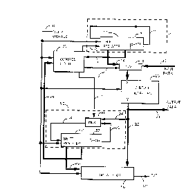
Figure 1 is a blocK diagram of a test circuit in
accordance with the invention; and
Figure 2 is a schematic block diagram of a portion
of the test circuit shown in Figure 1.
IA Figures 1 and 2, a linear feedback shift
register (LFSR) 5 for generating pseudo random test data is
shown comprising a conventional shift register 10 coupled to
an exclusi~e-or gate 13. A multiplexer circuit 15 is adapted
to selectively connect the input ports of a circuit under
test 20 via a data bus 14 or to a data inp~t bus 17 under
control of signals 31 from control circuit 30. In more
detail, Figure 2 shows the LFSR S comprised of a 15-bit shift
register 10 and an exclusive-or gate 13. The first 10 stages
3s of the 15-bit shift register correspond to bit positions 1 to
10 and provide a 10 bit parallel output stream of pseudo
random test data on data bus 14. The exclusive-or gate 13 is
connected to receive the values stored in two locations
(e.g., 14th and 15th bit positions) of the 15-bit shift

20~7~7
register and generates an exclusive-or feedback signal which
is transmitted on feedback path 12 to the input stage of the
shift register 10. The circuit under test 20 receives the
test patterns from the LFSR 5 and provides the test patterns
on bus 22. As mentioned above, the circuit of the invention
is particularly well suited to the testing of a circuit such
as a switching network which of course comprises a plurality
of transmission paths. The multiplexer 15 is thus arranged
to switchably connect the test signals from the LFSR 5 or the
normal input data on bus 17 to the various input ports of the
switching network. Data bus 21 connected to bus 22 provides
ouL~L data to other circuitry connected to the circuit under
test 20. The data transmitted on data bus 21 is either
normal input data which originated on data bus 17 or the
input test data originating from the LFSR 5.
A second LFSR circuit 50 is configured in a similar
-nner as the first; however, a multiplexer 40 permits one of
two signals to be fed back to the input stage of a shift
register 51. An exclusive-or gate 53 is responsive to the
two most significant bits of the shift register 51, (e.g.,
bits 14 and 15), to generate an exclusive-or feedback signal
which is transmitted on feedback path 52 to the multiplexer
40 which is also cor.nected to data line 24 to receive a
signal carried on the least significant data line of data bus
22. The control circuit 30 provides a selection control
signal on control line 34 for selecting the signal carried on
data line 24 or the feedback signal carried on feedback path
52. The least significant data line on data bus 22 is
connected to data line 24 to permit a portion of the pseudo
random data transmitted in the least significant bit position
to be transmitted to the second LFSR 50 via the multiplexer
40. The control circuit also monitors the value stored in
the LFSR 5 and the LFSR 50 via control lines 16 and 19
respectively.
A comparator 60 is connected to receive the 10-bit
series of output test patterns from the circuit 20 and a
10-bit pattern generated by the second LFSR circuit 50 on

2~7~47
data bus 58. The comparator 60 compares the two 10-bit
series of test patterns and generates true or false signals.
A clock signal provided on control line 18 provides a timing
signal to the first LFSR 5, the control circuit 30, the
second LFSR circuit 50 and to the comparator 60. If that
clock signal has the same frequency as that normally driving
the circuit under test 20, then the circuit is exercised
under real-life conditions.
In operation, the LFSR S is adapted to generate
pseudo random binary test data for provision to the circuit
under test 20. After a sequence of 215-l patterns have been
generated by the LFSR 5 the sequence of patterns repeats.
Upon power up of the test circuitry, the control
circuit 30 initializes the 15-bit binary value stored in the
LFSR 5 to a non-zero value to prevent the LFSR 5 from
generating only zero-bit patterns. After initialization, the
control circuit 30 continues to monitor the contents of the
first and second LFSRs 5 and 50 to ensure that they do not
remain in a state where either one of them contains all zero
bits. If an all zero state is detected in the LFSR 5 or the
LFSR 50, the control circuit 30 re-initializes the test
circuit by asserting the signals on control lines 32 and 34.
Once the LFSR 5 has been initialized, the binary
word stored in the 15-bit shift register 10 is shifted in the
more significant direction in a rotational manner; the bit
stored in the first stage of the shift register 10 is shifted
to the second stage; the bit stored in the second stage is
simultaneously shifted to the third stage, and so on. Each
shift occurs synchronously with each period of the clock
signal. As each shift occurs, the bits stored in the two
most significant bit positions, bits 14 and 15 are
exclusive-ored and the resultant signal is fed back to the
least significant bit position of the shift register 10.
Feeding back the resultant signal ensures that, with each
period of the clock signal, the binary value of the 15-bit
binary word in the LFSR 5 changes with each shift. The least

2a~74~7
significant 10 bits of the 15-bit binary word corresponding
to the first 10 stages of the shift register, form a binary
pattern and with each shift, a different pattern is formed.
Of course, the entire 15 bits could be used to form test
patterns, however, in the embodiment described only the least
10 significant bits are required. Providing an LFSR which
has more register stages than the bits used for the test
patterns as exemplified in the embodiment, provides more
patterns in the series of test patterns and thus provides a
greater variation of stimuli presented to the circuit under
test. The series of pseudo random binary data patterns are
transmitted to the circuit under test 20 via data bus 14 and
multiplexer 15.
After a transmission delay in the circuit under
test 20, the comparator 60 is presented with the first
patterrl via data bus 2Z. During the initialization stage,
the selection control signal is asserted on control line 34
to select a least significant bit of the series of patterns
transmitted on data bus 22 to provide an input signal to the
second LFSR circuit 50. After 15 clock cycles have occurred,
a 15-bit word corresponding to a word that was generated in
the first LFSR 5 will have been written into the second LFSR
circuit 50. By copying 15 successive values from the least
significant data line of data bus 22, and shifting the 15
bits into the second LFSR 50, a 15-bit word is captured which
was generated sometime before in the first LFSR 5. The
15-bit binary word in the LFSR 50 represents a seed value
from which it may generate data patterns on its own in a free
running mode. The control circuit 30 thus de-asserts the
selection control signal on control line 34 and the
multiplexer 40 provides the input stage of the second LFSR 50
with the exclusive-or feedback signal carried on feedbac~
path 52. With each successive period of the clock signal, a
10-bit binary word corresponding to the least significant
10-bits of the second LFSR 50 are presented to the comparator
60. Each 10-bit binary word presented to the comparator 60
on data bus 58 should henceforth match a pattern of the
series of patterns received on data bus 22. A mismatch

2 ~ ~ 7 ~ ~ 7
between the two 10-bit binary words presented to the
comparator 60 results in the comparator generating a false
condition signal on an output line 62. A mismatch indicates
that a 10-bit pseudo random binary pattern has become altered
during transmission through the circuit under test 20.
Corrective action may be taken on each error detection or
statistics of false conditions may be logged and corrective
action taken when the number of false conditions exceeds an
acceptable predetermined number.
The invention thus provides a simple and economical
circuit and method of verifying the integrity of a
tr~n~ ission path. Since the circuit uses only digital logic
circuitry, it may be readily implemented as an integrated
circuit either on its own or as a portion of another
integrated circuit. In addition, the circuit may be driven
by the same clock signal source as that of the circuit under
test thus providing real life test conditions.
Numerous other modifications, variations and
adaptations may be made to the particular embodiment of the
invention described above without departing from the scope of
the claims.

Dessin représentatif
Une figure unique qui représente un dessin illustrant l'invention.
États administratifs

2024-08-01 : Dans le cadre de la transition vers les Brevets de nouvelle génération (BNG), la base de données sur les brevets canadiens (BDBC) contient désormais un Historique d'événement plus détaillé, qui reproduit le Journal des événements de notre nouvelle solution interne.

Veuillez noter que les événements débutant par « Inactive : » se réfèrent à des événements qui ne sont plus utilisés dans notre nouvelle solution interne.

Pour une meilleure compréhension de l'état de la demande ou brevet qui figure sur cette page, la rubrique Mise en garde , et les descriptions de Brevet , Historique d'événement , Taxes périodiques et Historique des paiements devraient être consultées.

Historique d'événement

Description Date
Exigences relatives à la révocation de la nomination d'un agent - jugée conforme 2021-04-01
Inactive : CIB désactivée 2015-03-14
Inactive : CIB du SCB 2015-01-17
Inactive : CIB expirée 2015-01-01
Le délai pour l'annulation est expiré 2006-12-11
Inactive : Demande ad hoc documentée 2006-02-23
Lettre envoyée 2005-12-12
Inactive : TME en retard traitée 2003-11-25
Lettre envoyée 2000-10-13
Lettre envoyée 1999-07-22
Accordé par délivrance 1998-12-29
Inactive : Taxe finale reçue 1998-09-03
Préoctroi 1998-09-03
Un avis d'acceptation est envoyé 1998-08-27
Lettre envoyée 1998-08-27
Un avis d'acceptation est envoyé 1998-08-27
Inactive : Renseign. sur l'état - Complets dès date d'ent. journ. 1998-08-20
Inactive : Dem. traitée sur TS dès date d'ent. journal 1998-08-20
Inactive : Approuvée aux fins d'acceptation (AFA) 1998-07-02
Inactive : CIB attribuée 1998-07-02
Inactive : Supprimer l'abandon 1998-04-06
Réputée abandonnée - omission de répondre à un avis sur les taxes pour le maintien en état 1997-12-11
Toutes les exigences pour l'examen - jugée conforme 1993-11-24
Exigences pour une requête d'examen - jugée conforme 1993-11-24
Demande publiée (accessible au public) 1993-06-12

Historique d'abandonnement

Date d'abandonnement Raison Date de rétablissement
1997-12-11

Taxes périodiques

Le dernier paiement a été reçu le 1998-11-12

Avis : Si le paiement en totalité n'a pas été reçu au plus tard à la date indiquée, une taxe supplémentaire peut être imposée, soit une des taxes suivantes :

  • taxe de rétablissement ;
  • taxe pour paiement en souffrance ; ou
  • taxe additionnelle pour le renversement d'une péremption réputée.

Les taxes sur les brevets sont ajustées au 1er janvier de chaque année. Les montants ci-dessus sont les montants actuels s'ils sont reçus au plus tard le 31 décembre de l'année en cours.
Veuillez vous référer à la page web des taxes sur les brevets de l'OPIC pour voir tous les montants actuels des taxes.

Historique des taxes

Type de taxes Anniversaire Échéance Date payée
TM (demande, 6e anniv.) - générale 06 1997-12-11 1997-12-10
Taxe finale - générale 1998-09-03
TM (demande, 7e anniv.) - générale 07 1998-12-11 1998-11-12
TM (brevet, 8e anniv.) - générale 1999-12-13 1999-11-04
TM (brevet, 9e anniv.) - générale 2000-12-11 2000-08-25
TM (brevet, 10e anniv.) - générale 2001-12-11 2001-12-11
TM (brevet, 11e anniv.) - générale 2002-12-11 2002-12-11
TM (brevet, 12e anniv.) - générale 2003-12-11 2003-11-25
TM (brevet, 13e anniv.) - générale 2004-12-13 2004-12-10
2004-12-10
Titulaires au dossier

Les titulaires actuels et antérieures au dossier sont affichés en ordre alphabétique.

Titulaires actuels au dossier
NORTEL NETWORKS LIMITED
Titulaires antérieures au dossier
JOHN ALBERT GAUTHIER
JOHN KENNETH GOATCHER
Les propriétaires antérieurs qui ne figurent pas dans la liste des « Propriétaires au dossier » apparaîtront dans d'autres documents au dossier.
Documents

Pour visionner les fichiers sélectionnés, entrer le code reCAPTCHA :


Pour visualiser une image, cliquer sur un lien dans la colonne description du document (Temporairement non-disponible). Pour télécharger l'image (les images), cliquer l'une ou plusieurs cases à cocher dans la première colonne et ensuite cliquer sur le bouton "Télécharger sélection en format PDF (archive Zip)" ou le bouton "Télécharger sélection (en un fichier PDF fusionné)".

Liste des documents de brevet publiés et non publiés sur la BDBC .

Si vous avez des difficultés à accéder au contenu, veuillez communiquer avec le Centre de services à la clientèle au 1-866-997-1936, ou envoyer un courriel au Centre de service à la clientèle de l'OPIC.

({010=Tous les documents, 020=Au moment du dépôt, 030=Au moment de la mise à la disponibilité du public, 040=À la délivrance, 050=Examen, 060=Correspondance reçue, 070=Divers, 080=Correspondance envoyée, 090=Paiement})


Description du
Document 
Date
(aaaa-mm-jj) 
Nombre de pages   Taille de l'image (Ko) 
Dessin représentatif 1998-12-23 1 7
Dessin représentatif 1998-10-12 1 13
Revendications 1998-06-16 5 211
Dessins 1998-06-16 2 25
Dessins 1993-12-19 2 21
Revendications 1993-12-19 5 180
Abrégé 1993-12-19 1 20
Description 1993-12-19 8 329
Avis du commissaire - Demande jugée acceptable 1998-08-26 1 166
Avis concernant la taxe de maintien 2006-02-05 1 172
Taxes 2002-12-10 1 32
Correspondance 1997-12-09 2 58
Correspondance 1998-09-02 1 36
Correspondance 2000-02-07 1 22
Taxes 1999-11-03 1 33
Taxes 2001-12-10 2 71
Taxes 1998-11-11 1 39
Taxes 1997-12-09 1 36
Taxes 2000-08-24 1 31
Taxes 2004-12-09 2 66
Correspondance 2006-03-07 2 132
Taxes 1996-11-26 1 44
Taxes 1994-11-29 1 46
Taxes 1993-11-23 1 45
Taxes 1995-11-14 1 49
Correspondance de la poursuite 1991-12-10 13 550
Correspondance de la poursuite 1993-11-23 1 31
Correspondance de la poursuite 1993-11-23 1 38
Correspondance de la poursuite 1994-02-22 1 38
Correspondance de la poursuite 1994-02-22 1 18
Demande de l'examinateur 1997-07-07 2 48
Correspondance de la poursuite 1998-01-06 2 47
Correspondance de la poursuite 1998-03-31 1 26
Courtoisie - Lettre du bureau 1998-04-01 2 33
Courtoisie - Lettre du bureau 1993-12-23 1 35