Note : Les descriptions sont présentées dans la langue officielle dans laquelle elles ont été soumises.
206 1 349
_ .
BACKGROUND OF THE INVENTION
Field of the Inventlon
Thls inventlon relates to a surface-normal
optoelectronlc fuslon devlce to be used for highly parallel
optlcal transmlsslon and optlcal lnformatlon processlng or the
llke.
BRIEF DESCRIPTION OF THE DRAWINGS
Flg. 1 ls a cross-sectlonal vlew of a conventlonal
surface-normal optoelectronlc devlce;
Flg. 2 ls a cross-sectlonal vlew of a surface-normal
optoelectronlc devlce accordlng to a flrst embodlment of thls
lnventlon;
Flgs. 3 to 5 are for explalnlng a productlon method
of the devlce as shown ln Flg. 2 on a processlng basls ln
whlch:
Flg. 3 cross-sectlonally shows that a flrst
semlconductor layer, a second semlconductor layer, an actlve
layer, a thlrd semlconductor layer, a fourth semlconductor
layer and a contact layer are formed on a substrate ln thls
order, and that a part of the fourth semlconductor layer and a
part of the contact layer are removed thereafter to form a
mesa portlon thereon;
Flg. 4 cross-sectlonally shows that a Zn diffuslon
region ls formed ln the thlrd semlconductor layer, and
Fig. 5 cross-sectionally shows that hlgh-reslstance
reglons are formed ln the thlrd semlconductor layer;
Flg. 6 ls a cross-sectlonal vlew of a surface-normal
optoelectronlc devlce accordlng to a second embodlment of thls
- 1 - '~C
--~ 74646-2
inventlon. 2061 349
Descrlptlon of the Prlor Art
Such a surface-normal optoelectronlc fuslon devlce
that the lnput and output of a llght can be made ln the
dlrectlon perpendicular to the surface of a semlconductor
substrate and that possesses functlons lncludlng latch ls an
lndlspensable key device to be used for computer-to-computer
data transmlsslon and optlcal computlng. A conventlonal
surface-normal optoelectronlc fuslon devlce ls cross-
sectlonally shown ln Flg. 1. Thls devlce ls dlsclosed ln theJapanese Lald-Open Patent Publlcatlon No. 64-14963.
The conventlonal surface-normal optoelectronlc
fuslon devlce shown ln Flg. 1 has so-called pnpn structure, ln
whlch on a n-type GaAs substrate 60, a n-type AlGaAs layer 61
(Al composltlon ratlo 0.4; layer thlckness l~m; doplng
74646-2
206 1 349
concentratlon of donor 1 x 1018cm 3), a p-type GaAs layer 62
(layer thickness 50 ~; doplng concentratlon of acceptor 1 x
1019cm 3), a n-type GaAs layer 63 (layer thlckness lym; doplng
concentratlon of donor 1 x 1017cm 3), a p-type AlGaAs layer 64
(Al composltlon ratlo 0.4; layer thlckness 0.5ym; doplng
concentratlon of acceptor 1 x 1018cm 3), and a p-type GaAs
layer 65 (layer thlckness 0.15 ym; doplng concentratlon of
acceptor 1 x lO19cm 3) are lamlnatedly formed ln thls order.
The n-type GaAs layer 60 and n-type AlGaAs layer 61 constltute
a cathode range, the p-type GaAs layer 62 constltutes a p-type
gate range, the n-type GaAs layer 63 constltutes a n-type gate
range, the p-type AlGaAs layer 64 constltutes an anode range,
and the p-type GaAs layer 65 constltutes a contact layer.
The GaAs substrate 60 has a cathode electrode 66 of
an AuGe-Nl alloy formed on the surface (lower surface) on
opposlte surface of whlch the n-type AlGaAs layer 61 ls
formed, and on the upper surface of the p-type GaAs layer 65,
an anode electrode 67 of an Au-Cr-AuZn alloy ls formed. In
addltlon, a p-type dlffuslon range 68 ls provlded so as to
pass from the upper surface of the n-type GaAs layer 63
through the n-type GaAs layer 63 and p-type GaAs layer 62 to
~r 74646-2
206 ~ 349
the n-type AlGaAs layer 61. In the area ~ust above the p-type
dlffuslon reglon 68 on the upper surface of the n-type GaAs
layer 63, an n-type gate electrode 69 of an Au-Cr-AuZn alloy
ls formed, and a p-type gate electrode 70 of an AuGeNl alloy
ls formed on the upper surface of the n-type GaAs layer 63 on
the opposlte slde to the n-type gate electrode 69 wlth respect
to a mesa portlon formed on the surface of the n-type GaAs
layer 63.
In case of uslng the above-mentloned conventlonal
surface-normal optoelectronlc fuslon devlce, a blas voltage ls
applied so as to make the anode electrode 67 posltlve and the
cathode electrode 66 negatlve, and the value of thls blas
voltage ls set to a value ~ust before the devlce is turned on.
At thls tlme, a voltage ls not applled to the n-type gate
electrode 69 and p-type gate electrode 70. Next, when a
trlgger llght ls applled to the n-type gate electrode 69 or
the p-type gate electrode 70, the devlce ls turned on to
generate an output llght as shown ln Flg. 1. When once turned
on, it ls malntained even if the trigger llght ls stopped to
be applled. In thls case, lf the p-type AlGaAs layer 64
constltutlng the anode range, n-type AlGaAs layer 61
constltutlng the cathode range and n-type GaAs substrate
74646-2
206~ 349
are made larger in forbidden band width than the p-type
GaAs layer 62 constituting the p-type gate electrode and
n-type GaAs layer 63 constituting the n-typegate electrode,
carriers are confined into these gateranges, resulting
in an enhancement in luminous efficiency. In order to turn
it off, the polarity of the bias voltage to be applied to
the anode electrode 67 and the cathode electrode 66 is
reversed, and further, a voltage is applied so as to make
the n-type gate electrode 66 positive and the p-type gate
electrode 70 negative. As a result, the carriers confined
into these gate ranges shown above are forcibly taken out
of the device, so that it is turned off. This means that
high speed turn-off operation becomes possible.
With the conventional surface-normal optoelectronic
fusion device as shown in Fig.l, a light emission is made in
the light emitting diode (LED) mode under the turned-on
condition, being unsatisfactory in electro-optic conversion
efficiency. In addition, the turn-off time is as large as
several hundreds psec, so that it is required to do it more
speedy. Further in addition, because the gate electrodes 69
and 70 are provided, an electric current is expandingly
blowed not only to the range corresponding to a light
20 ~ 1 34~
emlttlng portlon (mesa portlon) of the p-type GaAs layer 62 as
an actlve layer but also to the range out of the same, whlch
means that the luminous efflclency cannot be lmproved. Also,
the natural emlsslon mode has a llmltatlon upon frequency
characterlstlc, thus becomlng lmposslble to operate lt at hlgh
speed.
Therefore, an ob~ect of thls lnventlon ls to provlde
a surface-normal optoelectronlc fuslon device which makes it
posslble to operate turn-on and turn-off motlons at hlgher
speed than would be provlded by the above-descrlbed
conventlonal surface-normal optoelectronlc fuslon devlce as
well as to obtaln hlgher lumlnous efflclency.
Another ob~ect of thls lnventlon ls to provlde a
surface-normal optoelectronlc fuslon devlce whlch ls operable
ln a laser dlode (LD) mode superlor ln electro-optlc
converslon efflclency.
SUMMARY OF THE INVENTION
Accordlng to a flrst aspect, the present lnventlon
provldes a semlconductor surface-normal optoelectronic devlce,
comprlslng: a semlconductor substrate; a flrst semlconductor
region of a first electroconductive type formed on sald
substrate; a second semiconductor region of a second
electroconductive type having a polarity opposite to that of
the flrst electroconductlve type, whlch ls formed on said
flrst semiconductor region; a semiconductor actlve layer
formed on sald second semlconductor reglon; a thlrd
semlconductor reglon of the flrst electroconductlve type
formed on sald semlconductor actlve layer; a fourth
74646-2
~, ~
20~ ~ 3~9
semlconductor reglon of the second electroconductlve type
formed on sald thlrd semlconductor reglon; a cathode electrode
connected to one of sald flrst semlconductor reglon and sald
fourth semlconductor region; an anode electrode connected to
the other of sald flrst semlconductor reglon and sald fourth
semlconductor reglon; a flrst gate electrode connected to sald
second semlconductor reglon; a second gate electrode connected
to sald thlrd semlconductor reglon; and a hlgh electrlc
reslstance reglon that passes through sald actlve layer, that
surrounds a llght emlttlng reglon of sald actlve layer, and
that has an electrlc reslstance hlgher than that of the llght
emlttlng reglon; whereby an electrlc current flowing through
sald actlve layer ls restrlcted by sald hlgh electrlc
resistance reglon.
Accordlng to a second aspect, the present lnventlon
provldes a semlconductor surface-normal optoelectronlc devlce
comprlslng: a semlconductor substrate; a flrst semlconductor
layer of a flrst electroconductlve type formed on sald
substrate; a second semlconductor layer of a second
electroconductlve type havlng a polarlty opposlte to that of
the flrst electroconductive type, whlch ls formed on sald
flrst semlconductor layer; a thlrd semlconductor layer of the
flrst electroconductlve type formed on sald second
semlconductor layer; a fourth semlconductor layer of the
second electroconductlve type formed on sald thlrd
semlconductor layer; a cathode electrode connected to one of
sald flrst semlconductor layer and sald fourth semlconductor
layer; an anode electrode connected to the other of sald flrst
74646-2
206~ 349
-
semlconductor layer and sald fourth semlconductor layer; a
flrst gate electrode connected to said second semiconductor
layer; a second gate electrode connected to sald thlrd
semlconductor layer; and a hlgh electric resistance region
that is formed in a vicinity of a ~unction of said second and
third semiconductor layers, that surrounds a light emitting
region, and that has an electric resistance higher than that
of the light emittlng region; whereby an electric current
flowing through sald llght emitting reglon is restricted by
the high electric resistance region.
In this device, the active layer is provided between
the second and third layers and the high resistance
range/ranges ls/are formed vertically passing through the
active layer so as to surround its luminous range, so that an
ineffective current to be flowed out of the luminous range can
be
- 7a -
74646-2
206 ~ 349
extremely reduced, resulting in an improvement in luminous
efficiency. In addition, there is no excess pn junction
around the luminous range, and a parasitic capacity becomes
small, so that it can be operated at higher speed. Further
in addition, the gate electrodes can be formed without
expanding the area of the active layer. Still further in
addition, said high resistance range/ranges can be realized,
for example, by injecting an ion selectively into said third
layer in the layer thickness direction.
In this device, it is preferable that said first layer
and fourth layer respectively include layers serving to act
as a reflecting mirror to sandwich said active layer
therebetween. In this case, in addition, it is preferable
that the sum of the thicknesses of the semiconductor layers
( that is, second layer, third layer and active layer )
provided between the first and fourth layers is an integral
multiple of the in-medium wavelength of an emitted light
from said active layer. As a result, this device makes
possible to effect a laser emission under the turn-on
condition. In this case, an ineffective current can be
extremely reduced, it makes possible to effect the LD action
without increasing the emitting threshold current. The LD
_ ~ _
206 ~ 349
mode is superlor ln electrooplc convertlng efflclency, swltch-
off speed, frequency characterlstlc and dlrectlvlty of an
emltted llght beam to the LED mode, whlch means that the
devlce of thls lnventlon can be made further superlor ln
varlous characterlstlcs to conventlonal ones. As the layer
servlng to act as a reflectlng mlrror, a multllayer fllm (of
p-type or n-type) made, for example, of a GaAs fllm and AlAs
fllm alternately lamlnated can be used.
It ls preferable that a part of sald thlrd layer ls
exposed from sald fourth layer to form sald flrst and second
gate electrodes on the surface of thus exposed part thereof
and sald hlgh reslstance ranges are respectlvely placed under
these gate electrodes.
Sald cathode electrode ls connected to sald flrst
layer or fourth layer accordlng to the electroconductlve type,
but lt may be connected dlrectly to sald flrst layer or fourth
layer or to the contact layer formed ad~acently to sald flrst
or fourth layer. The anode electrode ls slmllar to the above.
The electrode to be connected to sald flrst layer may be
connected to the substrate, ln thls case, however, lt ls
preferable to form a contact layer between sald substrate and
sald flrst layer for connectlng sald electrode to the
74646-2
206 1 349
contact layer thus formed. This is because the electrodes
are possibly formed only on one side of said substrate.
(2) In a second aspect, a surface-normal optoelectronic
fusion device of this invention features that it has a four-
layer structure which is obtained by excepting the active
layer from the device shown in the first aspect, and that
said second layer and third layer are smaller in forbidden
band width than said first layer or fourth layer, and that
high resistance range/ranges are provided at the vicinity of
the junction of said second and third layers so as to
surround its luminous range and have a resistance higher
than that of the luminous range.
In this device, similar to that of the first aspect, it
is preferable that a part of said third layer is exposed
from said fourth layer to form said first and second gate
electrodes on the surface of thus exposed part thereof, and
said high resistance range/ranges are placed under these
gate electrodes.
In this device, there is no active layer and the LD
action is not effected, however, the luminous range is
narrowed by the high resistance range/ranges similar to the
case in the first aspect, so that an electric current can be
- 2061 349
taken ln hlghly efflclently, resultlng ln obtalnlng a hlgher
llght output. In addltlon, there ls no excess parasltlc
capaclty due to pn ~unctlon around the lumlnous range, so that
hlgh speed response becomes posslble, resultlng ln an
lmprovement ln turn-off speed, for example, to several tens
psec.
DESCRIPTION OF THE PREFERRED EMBODIMENTS
Preferred embodlments of thls lnventlon wlll be
descrlbed below whlle referrlng to Flgs. 2 to 6.
[Flrst Embodlment]
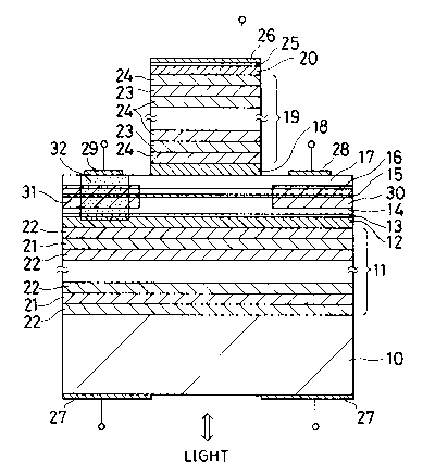
Flg. 2 cross-sectlonally shows a surface-normal
optoelectronlc fuslon devlce accordlng to a flrst embodlment
of thls lnventlon. In Flg. 2, on an n-type GaAs substrate 10,
an n-type semlconductor multllayer fllm 11 (doplng
concentratlon of donor 2 x 1013cm 3), an n-type AlGaAs layer
12 (doplng concentratlon of donor 2 x 1013cm 3; layer
thlckness 1500A; Al composltlon ratlo 0.4), a p-type AlGaAs
layer 13 (doplng concentratlon of acceptor 1 x 1019cm 3; layer
thlckness 50A; Al composltlon ratlo 0.25), a non-doped AlGaAs
layer 14 (layer thlckness about 1000A; Al
~ 74646-2
206 1 349
composition ratio 0.25), an active layer 15 having a
quantum well structure having laminated a non-doped InGaAs
layer (In composition ratio 0.2) and a non-doped AlGaAs
layer (Al composition ratio 0.25) (layer thickness each
100 A ; three periods), a non-doped AlGaAs layer 16 (layer
thickness about 1000 A; Al composition ratio 0.25), a non-
doped AlGaAs layer 17 ( doping concentration of donor 2 x
1017cm~3 ; layer thickness about 3000 A; Al composition
ratio 0.25), a p-type AlGaAs layer 18 (doping concentration
of acceptor 2 x 1018 cm~3 ; layer thickness 1500 A ; Al
composition ratio 0.4), a p-type semiconductor multilayer
film 19 (doping concentration of acceptor 2 x 1018cm~3), and
a p-type GaAs contact layer 20 ( doping concentration of
acceptor 1 x 1019cm~3) are laminatedly formed in this order.
The p-type AlGaAs layer 18, p-type semiconductor multilayer
film 19 and p-type GaAs contact layer 20 are formed in a
mesa portion.
Referring to the ten layers thus formed on the substrate
10, the n-type semiconductor multilayer film 11 and n-type
AlGaAs layer 12 constitute a first semiconductor layer
(cathod region), and the p-type AlGaAs layer 13 constitutes
a second semiconductor layer (p-type gate electrode). The
-- 206 1 349
non-doped AlGaAs layers 14 and 16 each serves to increase a
gain of transistor action during the operation of the
device. Referring to the active layer 15, the action as the
active layer on a strict sense basis is provided by the non-
doped InGaAs, and on the other hand, the non-doped AlGaAs
layer has the same action as each of the non-doped AlGaAs
layers 14 and 16 do. The n-type AlGaAs layer 17 constitutes
a third semiconductor layer (n-type gate region), and the p-
type AlGaAs layer 18 and p-type semiconductor multilayer
film 19 constitute a fourth semiconductor layer (anode
region).
The p-type AlGaAs layer 13 (second semiconductor layer)
and n-type AlGaAs layer 17 (third semiconductor layer)
having said active layer 15 sandwiched therebetween are made
larger in forbidden band width than said active layer 15. In
addition, the forbidden band width of the p-type AlGaAs
layer 13 is made smaller than that of the n-type AlGaAs
layer 12 (part of the first semiconductor layer) adjacently
formed to said layer 13. The forbidden band width of the n-
type AlGaAs layer 17 is made smaller than that of the p-type
AlGaAs layer 18 (part of the fourth semiconductor layer)
adjacently formed to said layer 17. As a result, carriers
2~16~1 3~
and a light can be easily confined thereto, so that laser
emission can be made easily, leading to a reduction in
threshold of luminescence.
The n-type semiconductor multilayer film 11 has n-type
GaAs layers 21 (layer thickness about 672 A ) and n-type
AlAs layer 22 (layer thickness about 804 A ) alternately
laminated. Here, 24.5 pairs of the layers 21 and 22 are
formed, in other words, 24 n-type AlAs layers 22 and 23 n-
type GaAs layers 21 are formed in an alternate lamination
manner. The p-type semiconductor multilayer film 19 has a p-
type GaAs layer 23 (layer thickness about 672 A ) and a p-
type AlAs layer 24 ( layer thickness about 804 A )
alternately laminated. In this case, 15.5 pairs of the
layers 23 and 24 are formed, in other words, 15 p-type AlAs
layers 24 and 14 p-type GaAs layers 23 are formed in an
alternate lamination manner. The layer thicknesses shown
above correspond to the quarter-wavelengths of a light
in respective media (layers). The multilayer films 11 and 19
each serves to act as a reflecting film of a light. The
distance between the films 11 and 19 is preferable to be
an integral multiple of the in-medium wavelength of an
emitted light in order to make emission easy. In this
- 14 -
-- 206 1 349
embodiment, the distance from the center line of the active
lager 15 to the multilayer film 19 is made two times the in-
medium wavelength of an emitted light, or about 5800 A , and
the distance from the center line of the active layer 15 to
the multilayer film 11 is made equal to the in - medium
wavelength thereof, or about 2900 A .
In the p-type GaAs contact layer 20 of the mesa portion,
an anode electrode consisting of a Cr layer 25 and an Au
layer 26 is formed. On the lower surface of the substrate
10, that is, the surface thereof opposite to the surface on
which the multilayer film 11 is formed, a cathode electrode
made of an AuGeNi/Au layer 27 is formed excepting a window
formed at the center thereof for taking out a light
therefrom. The n-type AlGaAs layer 17 is exposed around the
cylindrical mesa portion with a diameter of about 10~ m and
on thus exposed surface of the n-type AlGaAs layer 17, a n-
type gate electrode 28 made of an AuGeNi/Au layer and a p-
type gate electrode 29 made of a Cr/Au layer are formed. The
n-type gate electrode 28 and p-type gate electrode 29 are
disposed on the opposite side to each other with respect to
the mesa portion.
Within the n-type AlGaAs layer 17 ( third semiconductor
- 15 -
- 206 1 34 9
layer), non-doped AlGaAs layer 16, the active layer 15 and
non-doped AlGaAs layer 14, as shown in Fig . 2 , high
resistance ranges 30 and 31 are formed substantially just
below the gate electrodes 28 and 29, respectively. The high
resistance ranges 30 and 31 are provided such that in the
upper direction, or in the direction perpendicular to the
surface of the substrate 10, within the n-type AlGaAs layer
17, there exist only at the vicinity of the active layer 15,
within the non-doped AlGaAs layer 16 and active layer 15,
there exist over the whole thickness ranges thereof, and
within the non-doped AlGaAs layer 14, there exist over the
whole upper part excepting its one part on the side of the
p-type AlGaAs layer 13 (second semiconductor layer). The
section of the active layer 15 provided between the high
resistance ranges 30 and 31 constitutes a luminous range.
Within the n-type AlGaAs layer 17, non-doped AlGaAs
layer 16, active layer 15, non-doped AlGaAs layer 14, p-type
AlGaAs layer 13 and n-type AlGaAs layer 12, as shown in Fig.
2, a p-type diffusion range 32 having diffused zinc (Zn)
atoms is formed passing through the high resistance range
31. The p-type diffusion range 32 constitutes a p-type gate
range. The p-type diffusion range 32 is formed to be
- 16 -
- 2061 349
attained from the upper surface of the n-type AlGaAs layer
17 to the upper area of the n-type AlGaAs layer 12.
Next, a production method of the device shown above will
be explained below.
First, by a molecular beam epitaxy (MBE) method, on the
n - type GaAs substrate 10, the n - type semiconductor
multilayer film 11, the n-type AlGaAs layer 12, the p-type
AlGaAs layer 13, the non-doped AlGaAs layer 14, the active
layer 15 of quantum well structure having the non - doped
InGaAs layers and non-doped AlGaAs layers laminatedly
formed, the non-doped AlGaAs layer 16, the n-type AlGaAs
layer 17, the p - type AlGaAs layer 18, the p - type
semiconductor multilayer film 19 and the p-type GaAs contact
layer 20 are formed in this order by growing epitaxially.
Next, the p - type GaAs contact layer 20, p-type
semiconductor multilayer film 19 and p-type AlGaAs layer 18
are subjected to mesa etching by a lithographic method to
form a cylindrical mesa with a diameter of about 10~ m,
which is shown in Fig.3. In this case, however, a square
pillar-shaped mesa of about 10~ m square may be formed
instead of the cylindrical mesa.
Next, as shown in Fig.4, a siO2 film 33 with a thickness
- 17 -
206 1 349
of about 0.3 ~ m is formed on the surface of said
semiconductor multilayer lamination body forming the
cylindrical mesa and then, an opening is formed in the siO2
film 33 at a predetermined position of the upper surface of
the n-type AlGaAs layer 17. Thereafter, the diffusion of Zn
atoms are carried out at 550 C. The Zn atoms are diffused
in the lower direction passing through the opening to form
the p-type diffusion region 32 as shown in Fig . 4. The
diffusion should be carried out so that the diffusion front
of the Zn atoms can pass through the p-type AlGaAs layer 13
as the p-type gate range. In this embodiment, the diffusion
front is attained to the central portion of the n-type
AlGaAs layer 12 formed beneath the p-type AlGaAs layer 13.
Next, a photoresist film (with a thickness of about 5
~ m) is formed only on the cylindrical mesa of said
semiconductor multilayer lamination body and then, the
lithography technology is applied to remove the SiOa film 33
excepting that formed on the cylindrical mesa. As a result,
on the cylindrical mesa, a mask consisting of the sio2 film
33 and a photoresist film 34 is formed as shown in Fig.5.
The photoresist film 34 is preferable to be hard-baked for
one hour at about 200 C. Subsequently, irradiation of
- 18 -
- 2061 349
proton (H+) is made toward said mask to inject the proton
thereto from the upper surface of the n-type AlGaAs layer 17
with no mask formed. As a result, the proton injection is
made so as to surround the cylindrical mesa to form an area
where the proton is injected. Such a range as is surrounded
by the area becomes a luminous range. The proton injection
is preferable to be carried out under the conditions of
acceleration voltage 50 keV and dose quantity 3 x 1014cm~2.
As a result, as shown in Fig. 5, the high resistance ranges
30 and 31 can be selectively formed only within the proton-
injected layers existing at a moderated depth. Accordingly,
there can be formed the high resistance ranges 30 and 31 at
only the vicinity of the active layer 15. In addition,
referring to the proton-injected ranges, the high resistance
range 31 is formed inside the p-type diffusion region 32 and
the high resistance region 30 is formed outside the same.
After proton injection, said mask is removed.
Then, said semiconductor multilayer lamination body is
annealed for thirty seconds at 475 C. Thereafter, the layer
27 made of AuGeNi/Au is formed by the vacuum deposition
technology on the lower surface of the substrate 10
excepting the window to be taken out a light therefrom to
-- 19--
206 1 349
make a cathode electrode. The Cr layer 25 and the Au layer
26 are laminated in this order by the vacuum deposition
technology on the upper surface of the p-type GaAs contact
layer 20 to make an anode electrode. Also, by the same
technology, an AuGeNi/Au layer is formed at a predetermined
position of the upper surface of the n-type AlGaAs layer 17
excepting the p-type diffusion range 32 to make the n-type
gate electrode 28, and a Cr/Au layer is formed on the upper
surface of the n-type AlGaAs layer 17 on the p-type
diffusion range 32 to make the p-type gate electrode 29. As
a result, the surface-normal optoelectronic fusion device
as shown in Fig.2 can be obtained.
In case of using such a device as shown above, a bias
voltage is applied so as to make the anode electrode
positive and the cathode electrode negative, and yet, the
value of this bias voltage is set to the value just before
the device is turned on. At this time, the gate electrodes
28 and 29 are not applied with a voltage. Under this
condition, if a light is sent from the window formed on the
lower surface of the substrate 10 into the device, it is
turned on to generate an output light as illustrated. When
once turned it on, if the light is stopped to be sent, the
- 20 -
206 ~ 349
turn-on condition is maintained to continue the light
emission. For turning it off, the polarity of a voltage to
be applied to the anode and cathode electrodes is reversed
and furthermore, a voltage is applied to the n-type gate
electrode 28 and p-type gate electrode 29 so as to make the
electrode 28 positive and the electrode 29 negative,
respectively. As a result, the carrier confined into the
device is forcibly taken out of it at high speed thereby
turning it off.
The device according to the first embodiment of this
invention advantageously features that high speed switching
operation can be made while a current level necessary to
emit a light under turn-on condition is being maintained
low, and that from the fact that it is operable in the LD
mode, a luminous efficiency can be improved, a light beam to
be emitted is superior in directivity, and yet the
compatibility to other devices and optical fibers is
outstandingly high.
In this embodiment, a n-type contact layer may be formed
between the substrate 10 and the n-type semiconductor
multilayer film 11. Therefore, a cathode electrode can be
formed on the n-type contact layer thus obtained, so that
2 0 6 1 3 4 9
the electrodes become possible to be formed only on one side
of a semiconductor wafer.
[Second Embodiment]
Fig.6 is a cross-sectional view of a surface-normal
optoelectronic fusion device according to a second
embodiment of this invention. In Fig. 6, a n-type AlGaAs
layer 41 ( Al composition ratio 0.4 ; layer thickness 1~ m;
doping concentration of donor 1 x 1013cm~3), a p-type GaAs
layer 42 (layer thickness 50 A; doping concentration of
acceptor 1 x 10l9 cm~3), a n-type GaAs layer 43 (layer
thickness 1~ m; doping concentration of donor 1 x 1017cm~3),
a p-type AlGaAs layer 44 (Al composition ratio 0.4; layer
thickness 0.5~ m ; doping concentration of acceptor 1 x 10¹³
cm~3) and a p-type GaAs layer 45 (layer thickness 0.2~ m;
doping concentration of acceptor 1 x 1019 cm~3) are
laminatedly formed in this order on a n-type GaAs substrate
40. An active layer as in the first embodiment is not formed
in this embodiment. The n-type AlGaAs layer 41 constitutes
a first semiconductor layer, the p-type GaAs layer 42
constitutes a second semiconductor layer, the n-type GaAs
layer 43 constitutes a third semiconductor layer, and the p-
type AlGaAs layer 44 constitutes a fourth semiconductor
206 1 349
layer. The p-type GaAs layer 45 is a contact layer. The
layers 41, 42, 43, 44 and 45 can be successively formed on
the substrate 40 by growing epitaxially by a molecular beam
epitaxy (MBE) method as in the first embodiment.
On the upper surface of the p-type GaAs contact layer 45
in a mesa portion, an anode electrode 47 is provided, and on
the lower surface of the substrate 10, a cathode electrode
46 is provided excepting a window formed at the center
thereof for taking out a light therefrom. The n-type GaAs
layer 43 has the surface exposed around the mesa portion
thereby to form a n-type gate electrode 50 and a p-type gate
electrode 49 thereon. The n-type gate electrode 50 and p-
type gate electrode 49 are disposed on the opposite side to
each other with respect to the mesa portion.
Within the n-type GaAs layer 43 (third semiconductor
layer), p-type GaAs layer 42 (second semiconductor layer)
and n-type AlGaAs layer 41 (first semiconductor layer), as
shown in Fig. 6 , two high resistance ranges 51 and 52 are
formed substantially just below the gate electrodes 49 and
50, respectively. The high resistance ranges 51 and 52
respectively include, in the vertical direction (layer
thickness direction), the total thickness of the p-type GaAs
206 1 349
layer 42, and the vicinal thickness ranges of the n-type
GaAs layer 43 and n-type AlGaAs layer 41 to the p-type GaAs
layer 42. That is, the ranges 51 and 52 are not formed in
the lower range than said vicinal thickness range of the n-
type AlGaAs layer 41 and in the upper range than said
vicinal thickness range of the n-type GaAs layer 43. The
section of the p-type GaAs layer 42 provided between the
high resistance ranges 51 and 52 becomes a luminous range.
A p-type diffusion range 48 is formed vertically passing
through the high resistance range 52 within the n-type GaAs
layer 43, p-type GaAs layer 42 and n-type AlGaAs layer 41 as
shown in Fig.6, which constitutes a p-type gate range. The
p-type diffusion range 48 is attained from the upper surface
of the n-type GaAs layer 43 to the vicinity of the center of
the n-type AlGaAs layer 41.
Said electrodes 46,47,49 and 50, high resistance ranges
51 and 52, and p-type diffusion range 48 may be formed by
the same method as is used in the first embodiment.
The p-type GaAs layer 42 and n-type GaAs layer 43 are
larger in forbidden band width than the n-type AlGaAs layer
41 and/or p-type AlGaAs layer 44, and the carriers are
confined into the p-type GaAs layer 42 and n-type GaAs layer
- 24 -
206 ~ 349
43 under the turn-on condition, resulting in an improvement
in luminous efficiency. As a result, the threshold of
luminescence can be reduced.
The device of this embodiment has a mesa portion as in
the first embodiment, which is different therefrom in that
the mesa etching is made as to etch the n-type GaAs layer 43
as the third semiconductor layer up to a moderate depth
thereby to have the n-type GaAs layer 43 existed at the root
of the mesa portion. In addition, the device of this
embodiment is different from that of the preceding
embodiment in that the high resistance ranges 51 and 52
formed by an ion injection method respectively are provided
at the vicinity of the junction of the p-type GaAs layer 42
and n-type GaAs layer 43, and there exists no active layer
as formed in the preceding embodiment.
A method of using the device of this embodiment is the
same as in the first embodiment. That is, if it is to be
turned on, a voltage is not applied to the gate electrodes
49 and 50, but a voltage is applied so as to make the anode
electrode 47 positive and the cathode electrode 46 negative,
and under this condition, a light is sent from the window
formed on the lower surface of the substrate 40 thereunto.
- 25 -
- 206 1 349
Thus, a light is emitted from the window on the lower
surface of the substrate 40. If it is to be turned off, the
polarity of a voltage to be applied to the anode electrode
47 and cathode electrode 46 is reversed, and a voltage is
applied thereto so as~to make the p-type gate electrode 29
negative and the n-type gate electrode 28 positive.
As explained above, the surface-normal optoelectronic
fusion device of this invention makes it possible to switch
it highly speedy as well as to provide agood luminous
efficiency as compared with conventional ones.
- 26 -