Note : Les descriptions sont présentées dans la langue officielle dans laquelle elles ont été soumises.
2~22~ 7739
FIELD OF T~HE INVENTION
This invention relates to various
5 electrostatic discharge ~hereafter referred to as
"ESD") protection devices for various semiconductor
chip packages (hereinafter re~erred to as "SCP") of the
type having a plurality of connector pins which are
either (a) continuously shorted and then, upon
10 insertion of the connector pins into complementary
receptacles, automatically unshorted or (b)
continuously shorted until the physical removal of the
ESD protection device from the SCP.
BACKGROUND OF THE INVENTION
For a plurality of connector pins of a SCP
which mates with a corresponding plurality of
receptacles in a connector, typically, a printed
20 circuit board, it is frequently necessary to short
together the connector pins of the SCP until they are
inserted into complementary receptacles in the
connector in order to protect the semiconductor's
circuitry ~rom ESD. Present ESD protection devices
25 consist primarily of ESD packaging of the SCP in
electrically conductive strips, pellets, boxes and
plastic tubing which provides effective ESD protection
until the User is about to inserts the connector pins
of the SCP into the complementary receptacles in the
30 connector. At that point, however, the User must
remove this ESD packaging from the SCP, thus rendering
the SCP vulnerable to ESD, in order to position and
insert the connector pins into the receptacles.
Accordingly, as the User inserts the connector pins of
35 the SCP into the receptacles, the semiconductor dies
housed within these SCP1s could be destroyed by ESD and
,,
, : ~
'
2~22~8
7739
would have to be replaced. Moreover certain types of
scPs typically EPROMs, UVPROMs, and DRAMs, are plug-in
devices which have connector pins which are repeatedly
inserted into and then removed from the receptacles.
5 These types of scPS re~uire ESD protection during the
repeated insertions into and removals from the
receptacles. Specifically, the connector pins of these
SCPs require ESD protection from the moment that their
connector pins are removed from the receptacles till
10 their connector pins are again inserted therein.
Consequently, a need still exists within the
semiconductor chip packaging industry for a true ESD
protection device, rather than ESD packaging, which
effectively protects the semiconductor die from ESD
15 until the connector pins of the SCP are inserted into
the receptacles of the connector and then protects the
semiconductor die from ESD again when the connector
pins are removed from their respective receptacles.
SVMMARY OF THE INVENTION
With the foregoing in mind, the primary
object of the present invention is to provide an ESD
protection device on a SCP which operates in a simple,
25 economical, and effective manner to automatically short
a plurality of connector pins together while the SCP is
disconnected from a connector.
It is a further object of the present
invention to provide an ESD protection device on a SCP
30 which operates to automatically open the shorts between
the plurality of connector pins upon the SCP's
connection to a connector which has not been
specifically adapted to effect such opening.
It is yet another object of the present
35 invention to provide an ~SD protection device on a SCP
which operates to automatically short a plurality of
: . ~ ,.,::. ,., : .
- . , ~:.: :
- ~ ,
: .
2~22~3
7739
connector pins until the ESD protection device is
physically removed ~rom the SCP.
According to this invention, the foregoiny
objects are achieved by several different ESD
5 pro-tection devices, each discussed below, which are
disposed on the top or bottom surface of a SCP.
The SCPs are of the type that have a top
surface, a bottom surface, and, disposed between the
top and bottom surfaces, a pl~lrality of interface
10 surfaces each having a plurality of substantially
parallel and evenly spaced apart connector pins
disposed thereon. Each connector pin comprises a first
portion extending outward from the interface surface, a
second portion of substantially the same width as the
15 first portion extending in a downward direction, a bent
portion interconnecting the first and second portions,
a third portion extending downward to its distal end,
and an interface portion interconnecting the second and
third portions.
In the first embodiment, the ESD protection
device comprises a base section secured to the bottom
surface of the SCP and a plurality of integral shorting
arms. The plurality of shorting arms extend outwardly
from the base section with their plurality of distal
25 end portions in spaced apart relationship with respect
to each other and being transversely disposed with
respect to the connector pins. Each shorting arm
comprises a first portion fixedly secured to the base
section and extending outwardly from tha bottom
30 surface, a knee portion which extends from the first
portion and below the interface portion of a respective
one of the connector pins to define a bend in the
shorting arm, and an intermediate portion which extends
from the bend towards the respective one connector pin
35 so that the distal end portion extends over the first
portion of the respective connector pin. Each shorting
.:: ,
~:
2~2~
7739
arm further comprises means for yieldably biasing the
shorting arm so as to urge its distal end portion
against the first portion of the respective one
connector pin thereby crea~ing an electrical connection
5 therebetween when the pluralil:y of connector pins are
not inserted into a complementary plurality of
receptacles. When the connecl:or pins are inserted into
the complementary receptacles/ each knee portion moves
towards the bottom surface of the SCP against i-ts
10 yieldable bias so as to disengage its distal end
portion from the first portion of a respective one of
the connector pins to break the electrical connection
therebetween. Finally, an adhesive disposed on the
base section or a pair of clips disposed on the ends of
15 the base section provide this ESD protection device
with a secure attachment to the SCP.
In the second embodiment, the ESD protection
device comprises a base section secured to the top
surface of the SCP and a plurality of shorting arms and
20 gripping members which are both integral to the base
section. The plurality of shorting arms extend
outwardly from the base section in spaced apart
relationship with respect to each other and in spaced
apart alignment with respect to the plurality of
25 connector pins. Each shorting arm has a first portion
which is integral to the base section and which extends
outwardly and downwardly from the base section to
define a transverse edge portion. Each transverse edge
portion engages the first portion of a respective one
30 of the connector pins so as to electrically connect the
shorting arm and the connector pin. Similarly, the
plurality of gripping members extend from integral
connection to the base section in an interdigitated
spaced apart relationship with respect to the plurality
35 of shorting arms so as to provide the base section with
support and stability against lateral movement. Each
,
2~622~
7739
gripping member has a *irst portion extending along the
top surface of the SCP and an integral second portion
which securely grasps the SCP at an interface surface.
Finally, an adhesive disposed on the base section or a
5 pair of clips disposed on the ends of the base section
provide this ESD protection device with a secure
attachment to the SCP.
In the third embodiment, the ESD protection
device comprises a base section secured to the top
10 surface of the SCP and a plurality of shorting arms and
gripping members which are both integral to the base
section. The plurality of shorting arms extend
outwardly from the base section with distal end
portions in spaced apart relationship with respect to
15 each other and in spaced apart alignment with respect
to the plurality of connector pins. Each shorting arm
has a first portion which is integral to the base
section and which extends outwardly from the base
section in an integral connection to a respective one
20 of the distal end portions. Moreover, each first
portion is wider than its distal end portion so as to
define a transverse edge portion. Similarly, the
plurality of gripping members extend from integral
connection to the base section in an interdigitated
25 spaced apart relationship with respect to the plurality
of shorting arms so as to provide the base section with
support and stability against lateral movement. Each
gripping member has a first portion extending along the
top surface of the SCP and an integral second portion
30 which securely grasps the SCP at an interface surface.
Each shorting arm further comprising means for
yieldably biasing the shorting arm so as to urge its
transverse edge portion against ~he first portion of
the respective one of the connector pins thereby
35 creating an electrical connection therebetween when the
plurality of connector pins are not inserted into a
,
; , :
:1 ' .
.
2~2~8 7739
complementary plurality of receptacles. When the
connector pins are inserted into the complementary
receptacles, each distal end portion o~ the shorting
arms moves towards the bottom surface of the ScP
5 against its yieldable bias so as to disengage its
transverse edge portion from its respective connector
pin to break the electrical connection therebetween.
Finally, an adhesive disposed on the base section or a
pair of clips disposed on the ends of the base section
10 provide this ESD protection device with a secure
attachment to the SCP.
In the fourth embodiment, the ESD protection
device comprises a plurality of electrically conductive
bars each disposed in an overlying relation with
15 respect to the plurality of connector pins extending
from each interface surface and a spring structure
mounted to the top surface of the SCP for urging the
plurality of conductive bars against the conductor
pins. The spring structure has a central pad securely
20 mounted with an adhesive to the top surface of the SCP
and a plurality of spring members integral to the
central pad and corresponding in number to the number
of electrically conductive bars. Each spring member
has an integral cantilevered portion fixedly secured at
25 one end to the central pad and extending outwardly
beyond the top surface and an integral pair of spaced
apart depending leg portions extending downwardly on
both sides of the respective plurality of connector
pins and beyond the bottom surface. Each corresponding
30 electrically conductive bar is securely mounted with an
adhesive to its corresponding cantilevered portion
adjacent to the interface between its cantilevered
portion and its pair of leg portions so as to
selectively engage its respective plurality of
35 connector pins on an interface surface. Each spring
member furth~er comprises means for biasing the spring
. . . : - ~. ..:
.
,
.
2~22~
7739
member to the cantilevered portion towards the top
surface of the SCP so as to urge the electrically
conductive bar associated therewith against its
respective connector pins thereby creating an
5 electrical connection therebetween when the SCP is not
positioned against a surface of a connector. When the
SCP is positioned against the surface of the connector,
each cantilevered portion moves away from the top
surface of the SCP against its yieldable bias so as to
10 disengage its electrically conductive bar from its
respective plurality of connector pins on the interface
surface to break the electrical connection
therebetween.
In the fifth embodiment, the ESD protection
15 device comprises a base section which may be overlaid
on and secured to the top surface of the SCP and a
plurality of shorting arms which are integral to the
base section. The plurality of shorting arms extend
outwardly from the base section with distal end
20 portions in spaced apart relationship with respect to
each other and in spaced apart alignment with respect
to the plurality of connector pins when the ESD
protection device is secured to the SCP. Each shorting
arm has a first portion which is integral to the base
25 section and which extends outwardly from the base
section in an integral connection to a respective one
of the distal end portions~ Moreover, each first
portion is wider than its distal end portion so as to
define at least one lateral edge portion which is
30 moveable into engagement with the first portion of at
least one respective connector pin. Each shorting arm
further comprises means for yieldably biasing the
respective shorting arm so as to urge the lateral edge
portions of adjacent pairs of shorting arms against the
35 first portion of respective ones of the connector pins
thereby creating an electrical connection therebetween
' ' " ' ' '' ~' ' : ,,
:.
',
2~22~8
7739
when the plurality o~ connector pins are not inserted
into a complementary plurality of receptacles. When
the connector pins are inserted into the complementary
receptacles, each distal end portion of the shorting
5 arms moves apart from its respec~ive connector pin
against its yieldable bias so as to disengage its
later~l edge portion from its respective connector pin
to break the electrical connection therebetween. A
pair of clips disposed on the ends of the base section
10 or an adhesive provide this ESD protection device with
a secure attachmPnt to the SCP. Finally, a stiffening
rib disposed integrally within the base section
provides stiffness to the base section while pull tabs
disposed on the ends of the stiffening rib provide for
15 the quick and easy removal of this ESD protection
device from the SCP.
In the sixth and seventh embodiments, the ESD
protection device comprises a base section which may be
overlaid on and secured to the top surface of the SCP
20 and a plurality of shorting arms which are integral to
the base section. The plurality shorting arms extend
outwardly from the base section in spaced apart
relationship with respect to each oth2r and in spaced
apart alignment with respect to the plurality of
25 connector pins when the ESD protection device is
secured to the SCP. Each shorting arm has a member
which is integral to the base section and which extends
outwardly and downwardly from the base section to
define at least one lateral edge portion which is
30 moveable into engagement with the first portion of at
least one respective connector pin. Each shvrting arm
further comprises means for yieldably biasing the
respective shorting arm so as to urge the lateral edge
portions of adjacent pairs of shorting arms against the
35 first portion of respective ones of the connector pins
thereby creating an electrical connection therebetween.
, ~. ~ ,
. ~ ~
''' .
2~2~
7739
In the seventh embodiment, thare are shown bifurcated
shorting arms where slots physically separate adjacent
lateral edge portions that were connected in the sixth
embodiment and these slots provide each adjacent
5 lateral edge portion with the ability to move
independently of the other so as to independently
engage the ~irst portion of their respective connector
pin. A pair of clips dispos~d on the ends of the base
section or an adhesive provide this ESD protection
10 device with a secure attachment to the SCP.
stiffening rib disposed integrally within the base
section provides stiffness to the base section while
pull tabs disposed on the ends of the stiffening rib
provides for the quick and easy removal of the ESD
15 protection device from the SCP.
In the eight and final embodiment, the ESD
protection device comprises a base section which may be
overlaid on and secured to the top surface of the SCP
and a plurality of shorting arms which are integral to
20 the base section. The plurality of shorting arms
extend outwardly from the base section in spaced apart
relationship with respect to each other and in an
overlying spaced apart relationship with respect to
corresponding ones of the plurality of connector pins.
25 Each shorting arm has a member which is integral to the
base section and which extends outwardly and downwardly
from the base section to define an integral
protuberance at its distal end which engages the second
portion of at least one of the connector pins. A pair
30 of clips disposed on the ends of the base section or an
adhesive provide this ESD protection device with a
secure attachment to the SCP while pull tabs disposed
on the ends of the stiffening rib provide for the quick
and easy removal of the ESD proteckion device from the
35 SCP~
9 , ~
.
2B622~8 7739
DESCRIPTION OF THE DRAWINGS
The novel features that are considered
characteristic of the invention are set forth with
5 particularity in the appended claims. The invention
itself, however, both as to its organization and its
method of operation together with other objects and
advantages thereof will be best understood from the
following description of the illustrated embodiment
10 when read in connection with the accompanying drawings
wherein:
Figure lA is an exploded perspective view of
an ESD protection device of thi.s invention disposed
below a SCP;
Figure lB is a perspective view of the ESD
protection device shown in Figure lA mated to the
bottom surface of the SCP shown in Figure lA;
Figure lC is a perspective view of the ESD
protection device-SCP sub assembly shown in Figure lB
20 mated to a printed circuit board;
Figure 2A is an exploded perspective view of
another ESD protection device of this invention
disposed above a SCP;
Figure 2B is a perspective view of the ESD
25 protection device shown in Figure 2A mated to the top
surface of the SCP shown in Figure 2A;
Figure 2C is a perspective view of the ESD
protection device-SCP sub-assembly shown in Figure 2B
mated to a printed circuit board;
Figure 3A is an exploded perspective view of
another ESD protection device of this invention
disposed above a SCP;
Figure 3B is a perspective view of the ESD
protection device shown in Figure 3A mated to the top
35 surface of the SCP shown in ~igure 3A;
:, :
~: ,
2~622~g
7739
Figure 4A is an exploded perspective view of
another ESD protection device of this invention
disposed above a SCP;
Figure 4B is a perspective view of the ESD
5 protection device shown in Fiqure 4A mated to the top
surface of the SCP shown in Fi.gure 4A;
Figure 4C i5 a perspective view of the ESD
protection device-SCP sub-assembly shown in Figure 4B
mated to a printed circuit board;
Figure 4D is a side view as seen alony line
4D-4D of Figure 4B of the ESD protection device mated
to the top surface of the SCP;
Figure 4E is a side view as seen along line
4E~4E of Figure 4C of the ESD protection device-SCP
15 sub-assembly mated to the printed circuit board;
Figure 5A is an exploded perspective view of
another ESD protection device of this invention
disposed above a SCP;
Figure 5B is a perspective view of the ESD
20 protection device shown in Figure 5A mated to the top
surface of the SCP shown in Figure 5A;
Figure 5C is a perspective view of the ESD
protection device-SCP sub-assembly shown in Figure 5B
mated to a printed circuit board;
Figure 6A is an exploded perspective vi~w of
another ESD protection device of this invention
disposed above a SCP;
Figure 6B is a perspective view of the ESD
protection device shown in Figure 6A mated to the top
30 surface of the SCP shown in Figure 6A;
Figure 7A is an exploded perspective view of
another ESD protection device of this invention
disposed above a SCP;
Figure 7B is a perspective view of the ESD
35 protection device shown in Figure 7A mated to the top
surface of the SCP shown in Figure 7A;
.
'
:
.
. .
~0~22~ 7739
Figure 8~ is an exploded perspective view of
another ESD protection device oE this invention
disposed above a 5CP; and
Figure 8B is a perspective view of the ESD
5 protection device shown in Figure 8A mated to the top
surface of the SCP shown in Figure 8A.
: . .:
,
, .
2~22~ 7739
LY~5~ SDL~LIn~ REFERRED EMBODIMENTS
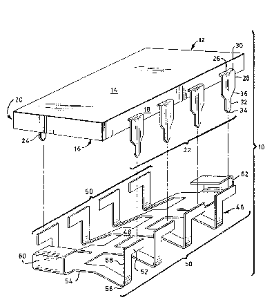
Referring now to FI~,U~ES lA-lC, there is
5 shown generally at 10 a SCP-ESD protection device
combination comprising an ESD protection device ~6 of
this invention, a SCP 12, and a complementary connector
38. The SCP 12 in one embodiment may comprise a top
surface 14, a bo~tom surface :16, and, between the top
10 and bottom surfaces, a pair o:E interface surfaces 18
and 20. A plurality of connector pins 22 and 24,
respectively, are disposed on each inter~ace surface 18
and 20, respectively, in a substantially parallel and
spaced apart relationship with respect to each other.
15 Each of the plurality of connector pins 22, 2~ further
comprises a first portion 26 extending outwardly from
the corresponding interface surface 18, 20, a second
portion 28 of substantially the same width as the first
portion 26 extending in a downward direction, a bent
20 portion 30 interconnecting the first portion 26 and the
second portion 28, a third portion 32 narrower than the
first portion 26 and extending downward to its distal
end 3~, and an interface portion 36 which interconnects
the second portion 28 and the third portion 32. ~s
25 will be readily understood, the SCP 12 may house either
a VLSI, LSI, or MSI semiconductor die or dies.
The plurality of the connector pins 22, 24
are adapted for physical and electrical connection to
the connector 38, typically a printed circuit board,
30 having a substantially planar surface 42 on one
selected side thereof. A plurality of elongated
receptacles 44 extend inwardly from the planar surface
42 in a subctantially parallel spaced apart insulated
relationship and in a complementary relationship with
35 respect to the connector pins 22, 24 so as to
accommodate the ready insertion of the third portion 32
'
;' . ' . :
2~22~ 7739
of the connector pins 22, 24 into the respective ones
of the receptacles 44.
In order to ensure that the connector pins
22, 24 are shorted until they are secured in the
5 complementary receptacles 44, the ESD protection device
46 is provided. This ESD protection device 46
comprises a hase section 48 secured to the botkom
surface 16 of the SCP 12 and a plurality of integral
shorting arms 50. The plurality of shorting arms 50
10 extend outwardly from the base section 48 with their
distal end portions 52 in spaced apart relationship
with respect to each othex and transversely disposed
with respect to the connector pins 22, 24,
respectively. Each shorting arm 50 comprises a first
15 portion 54 fixedly secured to the base section 48 and
extending outwardly from the bottom surface 16, a knee
portion 56 extending from the first portion 54 to
define a bend in the shorting arm below the interface
portion 36 of a respective one of the plurality of
20 connector pins 22, 24 and an intermediate portion 58
extending from the bend towards the respective one of
the plurality of connector pins 22, 24 so that the
distal and portion 52 extends over the first portion 26
of the respective one of the plurality of connector
25 pins 22, 24. An adhesive tnot ~hown) disposed on the
base section 48 or a pair of clips 60, 62 disposed on
the ends of the base section provides the ESD
protection device 4~ with a secure attachment to the
SCP 12.
The plurality of shorting arms 50 are
yieldably biased by any means well known in the art
such as a built in resilient spring bias so as to urge
their respective distal end portions 52 against the
first portions 26 of respective ones of the plurality
35 of connector pins 22, 24 th~reby creating an electrical
interconnection between the plurality of shorting arms
,
.. . . - . ,.
2~2 ~g 7739
50 and the plurality of connector pins 22, 24. Thus,
as is readily apparent from FIGURES lA-lC, when the
plurality of connector pins 22, 24 are not inserted
into the corresponding plurality of receptacles 44, the
5 shorting arms 50 urge their respective distal end
portions 52 against and into respective electrical
connection with the ~irst port:ions 26 of the respective
plurality of connector pins 22, 24. In this manner,
the shorting of all or some of the plurality of
10 connector pins 22, 24 is accomplished 50 as to
effectively protect the semiconductor die (not shown)
within the SCP 12 from ESD which could operate to
damage the electrical circuitry in the semiconductor
die.
Insertion of the connector pins 22, 24 into
the complementary receptacles 44 in the connector 38
operates to move and deflect upwards the knee portion
56 of the shorting arms 50 against their yieldable
bias, thereby moving the distal end portions 52 out of
20 physical and electrical connection with the first
portions 26 of the connector pins 22, 24, respectively.
As will be readily apparent, the number of
connector pins 22, 24 on either interface surface 18,
20 to be shorted together by this ESD protection device
25 46 need not include all the connector pins 22, 24 as
shown in FIGURES lA-lC but may also be limited to any
subset of all the conductive pins. Moreover, only a
subset of all the connector pins 22, 24 on just one
interface surface 18, 20 may be shorted together by
30 this ESD protection device 46 while all the other
connector pins 22, 24 remain unshorted.
Referring now to FIGURES 2A~2C where like
numerals designate previously described elements, there
is shown a second embodiment of the ESD protection
35 device 64 for the SCP 12' and the connector 38'. In
contrast to the first embodiment of the ESD protection
- .
:-.
'
2~224~
7739
dev.ice 46, this ~SD protection device 64 is disposed on
the top surface 14' of the S~P 12'. This unitary ESD
protection device 6~ comprises a base section 66
secured to the top surface 1~' of the SCP 12' and a
5 plurality of shorting arms 68 and grippiny mem~ers 70.
The plurality of shorting arms 68 extend outwardly from
the base section 66 with distal end portions 72 in
spaced apart relationship wit:h respect to each other
and in spaced apart alignment with respect to the
10 plurality of connector pins 22', 24'. Each of the
plurality of shorting arms 68 has a first portion 74
which is integral to the base section 66 and which
extends outwardly from the base section 66 in an
integral connection to a respective one of the distal
15 end portions 72. Moreover~ each ~irst por-tion 74 is
wider than its distal end portion 72 so as to define a
transverse edge portion 76.
Similarly, the plurality of gripping members
70 extend from integral connection to the base section
20 66 in an interdigitated spaced apart relationship with
respect to the plurality of shorting arms 68 so as to
provide the base section 66 with support and stability
against lateral movement. Each o~ the gripping members
70 has a first portion 78 extending along the top
25 sur~ace 14' of the SCP 12' and an integral second
portion 80 which securely grasps the SCP 12' at one of
the interface surfaces 18', 20l. Furthermore, an
adhesive (not shown) disposed on the base section 66 or
a pair of clips 82, 84 disposed on the ends of base
30 section 66 provides the ESD protection device 64 with a
secure attachment to the SCP 12'.
The shorting arms 68 are yieldably biased by
means well known in the art such as a built in
resilient spring bias so as to urge their respective
35 transverse edge portions 76 against the first portions
26' of the plurality of connector pins 22', 24',
16
'. ' , ' :'
; ~ ~
~22~ 7739
respectively, thereby creating an electrical
interconnection between the plurality of shorting arms
68 and the plurality of connector pins 22', 24'. Thus,
as is readily apparent from FIGURES 2A-2C, when the
5 plurality of connector pins 22', 24' are not inserted
into the corresponding plurality of receptacles 44',
the shorting arms 68 urge their respective transverse
edge portions 76 against and into respective electrical
connection with the first portions 26' of the
10 respective plurality of connector pins 22', 24'. In
this manner, the shorting of all or some of the
plurality of connector pins 22', 24' is accomplished so
as to effectively protect the semiconductor die (not
shown~ within the SCP 12' from the ESD which could
15 operate to damage the electrical circuitry within the
semiconductor die.
Insertion of the connector pins 22', 24' into
the complementary receptacles 44' operates to move and
deflect upwards the distal end portions 72 of the
20 shorting arms 68 against their yieldable bias, thereby
moving -the transverse edge portions 76 out of
respective physical and electrical connection with the
first portions 26l of the connector pins 22', 24'.
As will be readily apparent, the number oE
25 connector pins 22', 24' on either interface surface
18', 20' to be shorted together by this ESD protection
device 64 need not include all the connector pins 22',
24' as shown in FIGURES 2A-2C bu-t may also be limited
to any subset of all the conductive pins~ Moreover,
30 only a subset of all the connector pins 22', 24' on
just one interface surface 18', 20' may be shorted
together by this ESD protection device 64 while all the
other connector pins 22', 24' remain unshorted.
Re:Eerring now to FIGURES 3A-3B where like
35 numerals designate previously described elements, there
is shown a third embodiment of the ESD protection
,
, ~
2 ~ ~
7739
device 88 for the SCP 12' and the connector 38'. This
third embodiment of the ESD protection device 88 is
substantially similar to the second ESD protection
device embodiment 64 described above. In contrast to
5 the second embodiment, the clips of the second
embodiment have been replaced with pull tabs 90, 92 so
that only the adhesive (not shown) on the base section
94 in cooperation with the gripping members 70' secure
this ESD protection device 88 to the top surface 14' of
10 the SCP 12l. Like the second embodiment, this ESD
protection device 88 comprises a base section 94
secured to the top surface 14' of the SCP 12' and a
plurality of shorting arms 96 and gripping members 70'
which are both integral to the base section 94. The
15 plurality of yripping members 70', just as in the
second ESD protection device embodiment, extend in an
interdigitated spaced apart relationship with respect
to the plurality of shorting arms 96 so as to provide
the base section 94 with support and stability against
20 lateral movement. Also, as in the second embodiment,
each of the plurality of gripping members 70' comprises
a first portion 78' extending along the top surface 14'
of the SCP 12' and an integral second portion 80' which
securely grasps the SCP 12l at an interface surface
25 18', 20'.
The plurality of shorting arms 96, as in the
second embodiment, extend outwardly from the base
section 94 in spaced apart relationship with respect to
each other and in spaced apart alignment with respect
30 to the plurality of connector pins 22', 24'. Unlike
the second embodiment, however, each of the plurality
of shorting arms 96 has only an integral first portion
98 extending outwardly and downwardly from the base
section 94 to define a transverse edge portion 100
35 which engages the first portion 26' of a respective one
of the connector pins 22', 24'. This means that the
18
'
,
. , :
2~22~8 7739
transverse edge portions 100 always electrically
interconnect the shorting arms 96 to the plurality of
connector pins 22', 24', respectively, regardless of
whether or not the connector pins 22', 24' are inserted
5 into the complementary receptacles (not shown) of a
connector (not shown) because this embodiment lacks the
means for urging the transverse e~ge portions 100 away
from their correspondin~ first: portions 26'. Thus,
only the physical removal of this ESD protection device
10 88 from the top surface 14' of the SCP 12' by grasping
and pulling the pull tabs 90, 92 will electrically
disconnect the shortin~ arms g6 from the connector pins
22', 24'.
As was the case in the second ESD protection
15 device embodiment 64, the number of conneckor pins 22',
24' on either interface surface 18', 20' to be shorted
together by this third ESD protection device embodiment
88 need not include all the connector pins 22', 24' as
shown in FIGURES 3A-3B but may also be limited to any
20 subset of all the conductive pins. Moreover, only a
subset of all the connector pins 22', 24' on just one
interface surface 18', 20' may be shorted to~ether by
this ESD protection device 88 while all the other
connector pins 22', 24' remain unshorted.
Referring now to FIGURES 4A-4E, there is
shown generally at 102 another PC~-ESD protection
device combination of this invention comprising a
fourth ESD protection device embodiment, a SCP 104 and
a complementary connector 12~. The SCP 104 in one
30 embodiment may comprise a top surface 106, a bottom
surface (not shown), and, between the top and bottom
surfaces, a plurality of interface surfaces 108, 110,
112, 114. A plurality of connector pins 116, 1~8, 120,
122 are disposed on the interface surfaces 108, 110,
35 112, 114, respectively, in a substantially parallel and
spaced apart relationship with respect to each other.
19
J
~' , ~ ' ,
2~&22~8 7739
As will be readily understood, the SCP 104 may house
either a VLSI, LSI, or MSI semiconductor die or dies.
The plurality of connector pins 116, 118,
120, 122 are adapted for physical and electrical
5 connection to the connector 124, typically a printed
circuit board, having a subs~antially planar surface
126 on one selected side thereof. A plurality o~
surface pads 128 exist on the planar surface 126 in a
complementary relationship with respect to the
10 eonneetor pins 116, 118, 120, 122 so as to accommodate
the ready soldering of the connector pins 116, 118,
120, 122 to the respective ones of the surface pads
128.
In order to ensure that the connector pins
15 116, 11~, 120, 122 ara shorted until they are soldered
to the complementary surface pads 128, the ESD
protection device 130 is provided. This ESD protection
device 130 comprises a plurality of electrically
conductive bars 132, 134, 136, 138 disposed in
20 overlying relationship with respect to the plurality of
connector pins 116, 1189 120, 122 respectively and a
spring structure 140 mounted to the top surface 106 of
the SCP 104 for urging the plurality of conductive bars
132, 134, 136, 138 against the respectiYe conductor
25 pins 116, 118, 120, 122. The spring structure 140 has
a central pad 142 securely mounted with an adhesive
(not shown) to the top surface 106 of the SCP 104 and a
plurality of spring members 144, 146, 148, 150 integral
to the central pad 142 and corresponding in number to
30 the number of electrically conductive bars 132, 134,
136, 138. Each spring member 144, 146, 148, 150 has an
integral cantilevered portion 152 fixedly secured at
one end to the central pad 142 and extending outwardly
beyond the top surface and an integral pair of spaced
35 apart depending leg portions 154, 156 extending
downwardly on both sides of a respective one of the
': ~
,
,
2 ~ ~
7739
plurality of connector pins 116, 118, 120, 122 and
be~ond the bottom surface (not shown). Each
corresponding electrically conductive bar 132, 134,
136, 138 is securely mounted ~ith an adhesive (not
5 shown) to its corresponding cantilevered portion 152
adjacent to the inter~ace between its cantilevered
portion 152 and its pair of leg portions 154, 156 so as
to selectively engage its respective one of the
plurality of connector pins 116, 118, 120, 122.
The plurality of sp:ring members 144, 146, ..
148, 150 are yieldably biased by means well known in
the art such as an built in resilient spring bias so as
to urge their respective cantilevered portion 152
towards the top surface 106 and their respective
15 electrically conductive bars 132, 134, 136, 138 against
the connector pins 116, 118, 120, 122 respectively
thereby creating an electrical interconnection
therebetween. Thus, as is readily apparent from
FIGURES 4A-4E, when the plurality of connector pins
20 116, 118, 120, 122 are not soldered to their
complementary sur~ace pads 128, the spring members 144,
146, 148, 150 urge their respective electrically
conductive bar 132, 134, 136, 138 against and into
electrical connsction with their respective connector
25 pins 116, 118, 120, 122. In this manner, the shorting
of all of the connector pins 116, 118, 120, 122 is
accomplished so as to effectively protect the
semiconductor die (not shown) within the SCP 104 from
ESD which could operate to damage the electrical
30 circuitry in the semiconductor die.
Positioning the connector pins 116, 118, 120,
122 over the complementary surface pads 1~8 in the
connector 124 in readiness ~or soldering opera~es to
move and deflect upwards the leg portions 154, 156 of
35 all the spring members 144, 146, 148, 150 against their
yieldable bias, thereby moving all the electrically
21
.~ ~
.
- , :
2 ~622~ 7739
conductive bars 132, 134, 136, ~38 out of physical and
electrical connection with the connector pins 116, 118,
120, 122.
~s will be readily apparent, the connector
5 pins 116, 118, 120, 122 on all the interface surfaces
108, 110, 112, 114 need not be shorted together by this
ESD protection device 104 but may be limited to those
connector pins found in any select subset of all the
interface surfaces.
Referring now to FIGURES 5A-5C where like
numerals designate previously described elements, there
is shown a fifth embodiment o~ the ESD protection 158
for the SCP 12' and the connector 38'. This unitary
ESD protection device 158 comprises a base section 160
15 which may be overlaid on and secured to the top surface
14' of the SCP 12' and a plurality of shorting arms
162. The plurality of shorting arms 162 extend
outwardly from the base section 160 with distal end
portions 168 in spaced apart relationship with respect
20 to each other and in spaced apart alignment with
respect to the plurality of connector pins 22', 24'.
Each of the plurality of shorting arms 162 has a first
portion 166 which is integral to the base section 160
and which extends outwardly from the base section 160
25 in an integral connection to a respective one of the
distal end portions 168. Moreover, each first portion
166 is also wider than its distal end portion 16~3 so as
to define lateral edge portions 170.
A pair of clips 172, 174 are disposed on the
30 ends of the base section 160 of the ESD protection
device 158 which grip the top surface 14' and the
bottom surface 16' of the SCP 12' and secure the base
section 160 of the ESD protection device 158 to the top
surface 14' of the SCP 12'. Alternatively, an adhesive
(not shown) disposed on either base section 160 or the
top surface 14' of the SCP 12' can also provide the ESD
; ~ .: ,
, ! ,. . .
20G22~
7739
protection device 158 with a secure attachment to the
SCP 12'. A sti-~fening rib 176 is disposed integrally
within the base section 160 to provide stiffness to the
base section 160 so as to prevent lateral movement from
5 occurring in the base section 160 when the distal end
portions 168 of the shorting arms 162 move away from
their respective connector pins 22'. Cantilevered end
portions of the stiffening rib 176 extend beyond the
corresponding end portions of the base section 160 and
10 define a pair of pull tabs 17~3, 180 which provide for
the quick and easy removal of the ESD protection device
158 from the SCP 12'.
The shorting arms 162 are yieldably biased by
means well known in the art such as a built in
15 resilient spring bias so as to urge the lateral edge
portions 170 of adjacent pairs of shorting arms 162
against the first portions 26' of respective ones of
the connector pins 22', 24' thereby creating an
electrical interconnection between the plurality of the
20 shorting axms 162 and the plurality of connector pins
22', 24'. Thus, as is readily apparent from FIGURES
5A-5C, when the plurality of connector pins 22', 24'
are not inserted into the corresponding plurality of
receptacles 44', the shorting arms 162 urge their
25 respective lateral edge portions 170 against and into
electrical connection with the first portions 26' of
respective connector pins 22', 24'7 In this manner,
the shorting of all of the plurality of connector pins
22', 24' is accomplished so as to effectively protect
30 the semiconductor die (not shown) within the SCP 12'
from the ESD which could operate to damage the
electrical circuitry within the semiconductor die.
Insertion of the connector pins 22', 24' into the
complementary receptacles 44' operates to move and
35 deflect upwards the distal end portions 168 of the
shorting arms 162 against their yieldable bias, thereby
23
,
2~2~
7739
moving the lateral edge portions 170 out of physical
and electrical connection with the first portions 26'
of the connector pins 22', 24'.
As can be seen from FIGURES 5A-5C, the
5 shorting arms 162 at the ends of the base section 160
define only one lateral edge portion 170 while the
intermediate shorting arms 16:2 each define two lateral
edge portions 170 that engage respectively adjacent
connector pins 22', 24'. In this manner, each
10 connector pin 22', 24' is shorted by being engaged by
two lateral edge portions 170 from two adjacent
shorting arms ~62. This redundancy, as should be
readily apparent, operates to substantially improve the
reliability of the ESD protection device 158.
AS Will be readily apparent, the number of
connector pins 22', 24' to be shorted together by this
ESD protection device 158 need not include all the
connector pins 22', 24' as shown in FIGURES 5A-5C but
may also be limited to any subset of all the conductive
20 pins. Moreover, only a subset o~ all the connector
pins 22', 24' on just one interface surface 18', 20'
may be shorted together by this ESD protection device
158 while all the connector pins 22', 24' remain
unshorted.
Referring now to FIGURES 6A-6B and FIGURES
7A-7B where like numerals designate previously
described elements, there is shown a sixth and a
seventh embodiment of the ESD protection device 182 for
the SCP 12'. The distinguishing features between the
30 sixth and seventh embodiments are the slots 202,
explained below, found in the ESD protection device
shown in FIGURES 7A-7B but not in FI~URES 6A-6B. In
FIGURES 6 and 7, the ESD protection device 182
comprises a base section 184 secured to the top surface
35 14' of the SCP 12' and a plurality of shorting arms 186
which are integral to the base section 184. Just as in
24
.~ ~
~2~ 7739
the ESD protection device embodiment of FIGURE 5A-5C, a
pair of clips 188, 190 are disposed on the ends of the
base section 184 of the ESD protection device 182 which
grip the top surface 14' and the bottom surface 16' o~
5 the SCP 12' and secure the base section 184 of the ESD
protection device 182 to the top surface 14' of the SCP
12'. Alternatively, an adhesive (not shown) disposed
on either base section 184 or the top surface 14' of
the SCP 12' can also provide the ESD protection device
1~ 182 with a secure attachment to the SCP 12'. A
stiffening rib 192 is also disposed inteyrally within
the base section 184 and provides stiffness to the base
section 184 so as to prevent lateral movement from
occurring in the base section 184. Cantilevered end
15 portions of the stiffening rib 192 also extend beyond
the corresponding end portions of the base section 184
and define a pair of pull tabs 194, 196 which provide
for the quick and easy removal of the ESD protection
device 182 from the SCP 12'.
The plurality of shorting arms 186, as in the
embodiment of FIGURES 5A-5C, extend outwardly from the
base section 184 in a spaced apart relationship with
respect to each other and in a spaced apart alignment
with respect to the plurality of connector pins 22',
25 24'. Unlike the embodiment of FIGURES 5A-5C, however,
each of the plurality of shorting arms 186 has an
integral member 198 extending outwardly and downwardly
from the base section 184 to define at least one
lateral edge portion 200 which is moveable into
30 engagement with the first portion 26' of at least one
respective connector pin 22'. As can be seen from
FIGURES 6A-6B and FIGURES 7A-7B, the shorting arms 186
at the end of the base section 184 define only one
lateral edge portion 200 while the intermediate
35 shorting arms 186 each define two lateral edges 200
that engage respectively adjacent connector pins 22',
.
2~62~4~ 7739
24'. In this manner, each connector pin 22', 24' is
shorted by being engaged by two lateral edge portions
200 from two adjacent shorting arms 186. This
redundancy, as should be readily apparent, operates to
5 substantially improve the reliability of the ESD
protection device 182.
In FIGURES 7A-7B, t:here are shown bifurcated
shorting arms 186 where slots 202 physically separate
adjacent lateral edge portions 200 that were connected
10 in the embodiments of FIGURES 6A-6B. These slots 202
provide each adjacent lateral edge portion 200 with the
ability to move independently of the other 50 as to
independently engage the first portion 26' o~ their
respective connector pin 22', 24'. In FIGURES 6 and 7,
15 the lateral edge portions 200 always electrically
interconnect the shorting arms 186 to the plurality of
connector pins 22', ~4', regardless, of whether or not
the connector pins 22', 24' are insertsd into the
complementary receptacles (not shown) of a connector
(not shown~ because this embodiment lacks the means for
urging the lateral edge portions 200 away from their
respective first portions 26'. Thus, only the physical
removal of this ESD protection device from the top
surface 14' of the SCP 12' by grasping and pulling the
25 pull tabs 194, 196 will electrically disconnect the
shorting arms 186 from the connector pins 22', 24'.
As was the case in the ESD protection device
embodiment 158 of FIGURES 5A-5C, the number of
connector pins 22', 24' on either surface 18', 201 to
30 be shorted together by the ESD protection device
embodiment 182 of FIGURES 6A~6B and FIGURES 7A-7B need
not include all the connector pins 22', 24' but may
also be limited to any subset of all the connector
pins. Moreover, only a subset of all the connector
35 pins 22', 24' on just one interface surface 18', 20'
may be shorted together by this ESD protection device
26
;: ~ . . .
: ::
':,
~ ~ 6 ~ 7739
182 while all the other connector pins 22', 24' remain
unshorted.
Referring now to FIGURES 8A-8B where like
numerals designate previously described elements, there
5 is shown an eight and final embodiment of the ESD
protection device 204 for the SCP 12'. This ESD
protection device 204 comprises a base section 206
which can be secured to the top surface 14' of the ScP
12' and a plurality of shorting arms 208 which are
10 integral to the base section 206. A pair of clips
210, 212 are disposed on the ends of the base section
206 of the ESD protection device 204 and grip the top
surface 14' and the bottom surface :L6' of the SCP 12'
to sscure the base section 206 of thé ESD protection
15 device 204 to the top surface 14' of the SCP 12'.
Alternatively, an adhesive (not shown) disposed on
either base section 206 or the top surface 14' of the
SCP 12 ' can also provide the ESD protection device 204
with a secure attachment to the SCP 12'.
The plurality of shorting arms 208 extend
outwardly from the base section 206 in a spaced apart
relationship with respect to each other and in an
overlying spaced apart relationship with respect to
corresponding ones of the plurality of connector pins
25 22 ', 24 ' . Each shorting arrn 208 has a member 214 which
is integral to the base section 206 and which extends
outwardly and downwardly from the base section to
define an integral protuberance 216 at its distal end
218. Each member 214 is resiliently biased so that the
30 protuberance 216 at the distal end 218 thereof engages
and electrically shorts the second portion 28 ' of a
corresponding one of the connector pins 22 ', 24 ' . The
E:SD protection device 204 may also be removed from the
SCP 12' in the aforementioned manner by grasping and
35 pulling the pull tabs 220, 2220 Moreover, as will be
readily apparent, the width of an individual shorting
27
2 ~g224~ 7739
arm 206 in the ESD protection device 20a may be varied
so that the accompanying protuberance will short
together any subset of the connector pin 22', 24' on a
given interface surface 18', 20' at the same time.
Other embodiments of.` the invention includiny
additions, subtrac~ions, deletions, and other
modifications of the preferrecl disclosed embodiments of
the invention will be obvious to those skilled in the
art and are within the scop~ of the following claims.
28
' '
. ~ ~