Note : Les revendications sont présentées dans la langue officielle dans laquelle elles ont été soumises.
- 14 -
The invention claimed is:
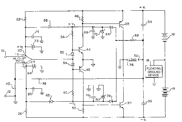
1. A power amplifier provided with overload
protection comprising, in combination, an input terminal
adapted to be connected to a source of electrical signals
and an output terminal adapted to be connected to a load,
power output means having an input and an output coupled
to the output terminal, an amplifier having an input
coupled to the input terminal and an output coupled to
the input of the power output means, said amplifier
having a supply voltage input, the output current of said
amplifier being a direct function of the potential on
said supply voltage input, a source of direct current
electrically connected to the supply voltage input to
said amplifier, said direct current source having a
potential at least equal to the potential required to
drive the amplifier to produce the current output to
excite the power output means to full output, and means
for switching a portion of the current from the source of
direct current from the supply voltage input of the
amplifier responsive to the load impedance falling below
a threshold value, whereby the amplifier reduces
excitation of the power output means when the load
impedance is below the threshold value and the power
output of the power output means is limited.
2. A power amplifier provided with overload
- 15 -
protection comprising the combination of claim l wherein
the means for switching a portion of the current from the
source of direct current from the supply voltage input of
the amplifier comprises a first diode and a second diode
connected in series opposition, the first diode being
connected to the supply voltage input of the amplifier to
conduct charges therefrom, and a resistor connected to
the load and in series with the first and second diodes,
the first and second diodes being back biased during
normal operation and conducting during periods in which
the load impedance is below a threshold value.
3. A power amplifier provided with overload
protection comprising the combination of claim 2 in
combination with a voltage regulator connected to the
voltage supply input of the amplifier to maintain a fixed
maximum potential thereon during periods of normal
operation.
4. A power amplifier provided with overload
protection comprising the combination of claim 3 wherein
the voltage regulator comprises a zener diode and a
capacitor connected in parallel.
5. A power amplifier provided with overload
protection comprising, in combination, an input terminal
- 16 -
adapted to be connected to a source of electrical signals
and an output terminal adapted to be connected to a load,
power output means having an input and an output coupled
to the output terminal, an amplifier having an input
coupled to the input terminal and an output coupled to
the input of the power output means, said amplifier
having a supply voltage input, and the output current of
said amplifier being a direct function of the potential
on said supply voltage input, a source of direct current,
means electrically connecting the source of direct
current to the supply voltage input of said amplifier
including a first resistive element, said direct current
source having a potential at least equal to the potential
required to drive the amplifier to produce the current
output to excite the power output means to full output, a
first diode and a second diode, each diode having a first
terminal and a second terminal and being polarized to
pass electrical current from the first terminal thereof
to the second terminal thereof, the first terminal of the
first diode being connected to the supply voltage input
of the amplifier and the second terminal of the first
diode being connected to the second terminal of the
second diode, capacitive means connected to the second
terminals of the first and second diodes, and a second
resistive element connected between the first terminal of
the second diode and the load terminal, the second diode
- 17 -
being reverse biased for load impedances higher than a
threshold value, whereby during periods in which the load
impedance is below the threshold value a portion of the
current from the direct current source is diverted from
the supply voltage terminal of the amplifier and the
potential on the supply voltage terminal is depressed,
thus limiting the current output of the amplifier and
reducing the current drive for the power output means.
6. A power amplifier provided with overload
protection comprising the combination of claim 5 wherein
the capacitive means connected to the second terminals of
the first and second diodes comprises a capacitor and a
voltage regulator connected in parallel.
7. A power amplifier provided with overload
protection comprising the combination of claim 6 wherein
the regulator comprises a zener diode.
8. A power amplifier provided with overload
protection comprising the combination of claim 5 in
combination with a transistor coupler electrically
connected between the amplifier and the power output
means, the transistor coupler having a base electrically
connected to the junction between the first and second
diodes and the current output of the transistor coupler
- 18 -
being directly related to the potential on the base
thereof, whereby during periods in which the load
impedance is below the threshold value, the second diode
becomes forward biased and conducts current from the load
to the junction between the first and second diodes, thus
reducing this potential and the potential on the base of
the transistor coupler to limit the output current
thereof.
9. A power amplifier provided with overload
protection comprising the combination of claim 8 in
combination with a voltage regulator connected to the
junction between the first and second diode to maintain a
fixed maximum potential thereon during periods of normal
operation.
10. A power amplifier provided with overload protection
comprising the combination of claim 9 wherein the voltage
regulator comprises a zener diode and a capacitor
connected in parallel.
11. A power amplifier provided with overload
protection comprising, in combination, an input terminal
adapted to be connected to a source of electrical signals
and an output terminal adapted to be connected to a load,
- 19 -
power output means including a pair of power output
devices having an input and an output coupled two the
output terminal, a balanced operational amplifier having
an input coupled to the input terminal and an output
electrically coupled to the input of the power output
means, said amplifier having two opposed supply voltage
inputs, and the output current of said amplifier being
direct function of the potentials on said supply voltage
inputs, a first source of direct current, means
electrically connecting the first source of direct
current to the first supply voltage input of said
operational amplifier including a first resistive
element, a second source of direct current, a second
means electrically connecting the second source of direct
current to the second supply voltage input of said
operational amplifier including a second resistive
element, said first and second direct current sources
having potentials at least equal to the potential
required to drive the operational amplifier to produce
the current output to excite the power output means to
full output, a first diode, a second diode, a third
diode and a fourth diode, each diode having a first
terminal and a second terminal and being polarized to
pass electrical current from the first terminal thereof
to the second terminal thereof, the first terminal of the
first diode being connected to the first supply voltage
- 20 -
input of the operational amplifier and the second
terminal of the first diode being connected to the second
terminal of the second diode, capacitive means connected
to the second terminals of the first and second diodes,
the first terminal of the third diode being connected to
the second supply voltage input of the operational
amplifier and the second terminal of the third diode
being connected to the second terminal of the fourth
diode, capacitive means connected to the second terminal
of the third and fourth diodes, and a second resistive
element connected between the first terminal of the
second diode and the first terminal of the fourth diode
and the load terminal, the second diode and the fourth
diode being reverse biased for load impedances higher
than a threshold value and forward biased for load
impedances below the threshold value, whereby during
periods in which the load impedance is below the
threshold value portions of the current from the direct
current sources are diverted from the supply voltage
terminals of the operational amplifier and the potential
on the supply voltage terminals are depressed, thus
limiting the current output of the amplifier and reducing
the current drive for the power output means.
12. A power amplifier provided with overload
protection comprising the combination of claim 11 in
- 21 -
combination with a coupler having a first and a second
transistor electrically connected between the operational
amplifier and the output means, the first transistor
having a base electrically connected to the junction
between the first and second diodes, and the second
transistor having a base electrically connected to the
junction between the third and fourth diodes, the current
output of the coupler being a direct function of the
potential on the bases of the first and second
transistors, whereby during periods in which the load
impedance is below the threshold value, the potentials of
the junctions between the first and second diode and
third and fourth diodes falls reducing the potentials on
the bases of the first and second transistors, thus
limiting the current output of the coupler and reducing
the current drive for the power output means.