Sélection de la langue

Search

Sommaire du brevet 2064148 

Énoncé de désistement de responsabilité concernant l'information provenant de tiers

Une partie des informations de ce site Web a été fournie par des sources externes. Le gouvernement du Canada n'assume aucune responsabilité concernant la précision, l'actualité ou la fiabilité des informations fournies par les sources externes. Les utilisateurs qui désirent employer cette information devraient consulter directement la source des informations. Le contenu fourni par les sources externes n'est pas assujetti aux exigences sur les langues officielles, la protection des renseignements personnels et l'accessibilité.

Disponibilité de l'Abrégé et des Revendications

L'apparition de différences dans le texte et l'image des Revendications et de l'Abrégé dépend du moment auquel le document est publié. Les textes des Revendications et de l'Abrégé sont affichés :

  • lorsque la demande peut être examinée par le public;
  • lorsque le brevet est émis (délivrance).
(12) Demande de brevet: (11) CA 2064148
(54) Titre français: RESEAU DE CONDENSATEURS DISCOIDAUX UTILISANT UN SUBSTRAT
(54) Titre anglais: CAPACITOR ARRAY UTILIZING A SUBSTRATE AND DISCOIDAL CAPACITORS
Statut: Réputée abandonnée et au-delà du délai pour le rétablissement - en attente de la réponse à l’avis de communication rejetée
Données bibliographiques
(51) Classification internationale des brevets (CIB):
  • H03H 7/075 (2006.01)
  • H01G 4/38 (2006.01)
  • H01R 13/66 (2006.01)
  • H03H 1/00 (2006.01)
(72) Inventeurs :
  • GLIHA, EDWARD R., JR. (Etats-Unis d'Amérique)
(73) Titulaires :
  • AMPHENOL CORPORATION
(71) Demandeurs :
  • AMPHENOL CORPORATION (Etats-Unis d'Amérique)
(74) Agent: MARKS & CLERK
(74) Co-agent:
(45) Délivré:
(22) Date de dépôt: 1992-03-26
(41) Mise à la disponibilité du public: 1992-10-02
Licence disponible: S.O.
Cédé au domaine public: S.O.
(25) Langue des documents déposés: Anglais

Traité de coopération en matière de brevets (PCT): Non

(30) Données de priorité de la demande:
Numéro de la demande Pays / territoire Date
678,147 (Etats-Unis d'Amérique) 1991-04-01

Abrégés

Abrégé anglais


ABSTRACT OF THE DISCLOSURE
A planar filter array includes a single monolithic alumina substrate having a
plurality of counter bores on each side connected by central bores to form passages
for insertion of connector pin contacts. The connecting bores contain ferrite beads
and the counter bores contain discoidal capacitors which sandwich the ferrite beads
to form pi filter circuits for filtering the pin contacts. Grounding electrodes on the
discoidal capacitors are soldered to a grounding layer or traces on the substrate to
provide a ground path for the filters.

Revendications

Note : Les revendications sont présentées dans la langue officielle dans laquelle elles ont été soumises.


I Claim:
1. A filter array comprising grounding means (2, 19) for electrically connecting
said first filter elements to an external ground; a planar substrate (1) having two
principal exterior surfaces on opposite sides of said substrate and a plurality of
counter bores (3, 4) in each of said two principal exterior surfaces, wherein
corresponding ones of said counter bores (3) on one side of said substrate are
connected to corresponding ones of said counter bores (4) on the other side of said
substrate by connecting bores (5) which communicate with respective counter
bores on each side of the substrate; and a plurality of first filter elements within
said counter bores, wherein said filter array is characterized in that said grounding
means are located primarily on said principal exterior surfaces of said substrate.
2. A filter array as claimed in claim 1, further characterized in that said array
comprises a plurality of second filter elements (15) within said connecting bores,
said first filter elements sandwiching said second filter elements.
3. A filter array as claimed in claim 1, further characterized in that said
grounding means comprises a conductive layer (2) on said principal exterior
surfaces of said substrate.
4. A filter array as claimed in claim 1, further characterized in that said
grounding means comprises conductive traces (2) on said principal exterior surfaces
of said substrate.
5. A planar filter array as claimed in claim 1, further characterized in that said
grounding means comprises solder (19) located between ground electrodes (23) on

said first filter elements and a conductive coating (2) on said principal exterior
surfaces of said substrate.
6. A filter array as claimed in claim 2, further characterized in that said second
filter elements are ferrite beads and said first filter elements are discoidal
capacitors, said first and second filter elements together forming pi filters for
contact pins (20) inserted through pin receiving bores in each of said first and
second filter elements.
7. A filter array as claimed in claim 6, further characterized in that said
grounding means includes an external common grounding electrode on each
principal exterior surface, and said capacitors comprise an outer ground electrode
(23) and an inner hot electrode (24), said hot electrode being soldered to said pins
and said outer ground electrode being soldered to one of said external common
grounding electrodes.
8. A filter array as claimed in claim 1, further characterized in that said first
filter elements are discoidal capacitors.
9. A planar filter array as claimed in claim 8, further characterized in that two
of said capacitors have different capacitance values from each other.
10. A planar filter array as claimed in claim 1, further characterized in that said
counter bores and connecting bores are cylindrical and said connecting bores are
smaller in diameter than said counter bores, such that annular shoulders (6) are
formed at inner surfaces of said counter bores to provide supporting means for said
first filter elements.
11. A planar filter array as claimed in claim 1, further characterized in that said
substrate is made of alumina.
12. A filter array as claimed in claim 1, further characterized in that said first
filter elements comprise means defining a central pin receiving bore in each first
filter element for receiving a connector contact pin (20), a live electrode (24)
located on a surface of each central pin receiving bore, and means (18) for
electrically connecting said live electrode to said contact pin.
13. A method of assembling a filter array for use in a connector, comprising the
steps of: providing a planar substrate (1) having two principal exterior surfaces;
forming a plurality of counter bores (3, 4) in each of said two principal exterior
surfaces; forming connecting bores (5) to connect corresponding ones of said
counter bores with each other, and characterized in that said method further
comprises the steps of:
applying a conductive layer (2) on each principal surface of said substrate
to form an external common ground electrode for filter elements (10) to be located
in said bores;
inserting second ones of said filter elements (15) into respective ones of said
connecting bores;
inserting first ones of said filter elements into respective ones of said
counter bores after inserting said second ones of said filter elements into said
connecting bores;

electrically connecting individual ground electrodes (23) on said first filter
elements to a respective one of said common ground electrodes.
14. A method as claimed in claim 13, wherein said step of electrically
connecting said individual ground electrodes to said common ground electrodes is
characterized by comprising the step of soldering.
15. A method as claimed in claim 13, further characterized in that it comprises
the step of providing said first filter elements in the form of discoidal capacitors.
16. A method as claimed in claim 13, further characterized in that it comprises
the step of providing said second filter elements in the form of ferrite filter beads.
17. A method of assembling a filter connector, comprising the steps recited in
claim 13, and further characterized in that said method comprises the steps of:
inserting a substrate into an electrically conductive connector shell (21); and
electrically connecting said common ground electrodes to said electrical
connector shell.
18. A method as claimed in claim 17, characterized in that it further comprises
the steps of inserting connector contact pins through central pin receiving bores in
said first and second filter elements and electrically connecting live electrodes in
said first filter elements to said contact pins.

11
19. A method as claimed in claim 18, further characterized in that the step of
electrically connecting live electrodes to said contact pins comprises the step of
soldering.
20. A method as claimed in claim 18, further characterized in that it comprises
the step of providing said first filter elements in the form of discoidal capacitors.
21. A method as claimed in claim 18, further characterized in that it comprises
the step of providing said second filter elements in the form of ferrite filter beads.
22. A filter array for use in a connector, comprising a support substrate (1)
having two principal exterior surfaces on opposite sides of said substrate and a
plurality of counter bores (3, 4) in each of said two principal exterior surfaces,
wherein corresponding ones of said counter bores (30) on one side of said
substrate are connected to corresponding ones of said counter bores (4) on the
other side of said substrate by connecting bores (5) which communicate with
respective counter bores on each side of the substrate; and a plurality of first filter
elements (10) within said counter bores, and characterized in that said support
substrate is a substantially non-conductive planar ceramic support substrate.

Description

Note : Les descriptions sont présentées dans la langue officielle dans laquelle elles ont été soumises.


,, .: ~ ', 1. .
2 ~
CAPACITC)R ARRAY UTlLlZlNt3 A SUBSTP~ATE
AND DISCC)IDAL CAPACITORS
BACI~GROUND OF THE INVENTlt:)N ~:
1. Fi~l~l of the Invention
The present învention relates to filtared electrical connectors of the type
utilizing planar monolithic filter arrays.
2. Description of Related Art
It is known to provida electrical filters in connoc~ors for the purpose of
protecting sensitivo components frorn transient currants and vol~ages which
develop in a transmission cable due to electromagnetic and radio frequency
interference. Such transients are generally hi~h frequency in nature, and therefora
capacitive or tuned pi circuits are used to shunt th~ transiants to ground wi~hout ~.
affecting the primary signal carried by the cablo. ~ '.
Conventional dasigns generally fall into one of two cat~gories: The first
category includes filter connectors in which monolithic capacitor blocks are used.
The capacitor blocks generally consis~ of a planar block of dielectric material with ::
- ,. ~ ..... . ~
..
:.~ . . ~:

interleaved ground and hot elactrodes arranged to be electricaliy csnnected withpins inserted through holes in the blocks. Such blocks are convenient but are
disadvanta~eous in that customizing of capaci~ances for individual pins is difficult,
due to limitations of the single dielectric material used for the block and also the
need for additional manufacturing steps and tooling. Moreover, if any one capacitor
is defective, th0 unit must be replaced. When oombinad with ferrite blocks or
tubes to form pi filters, problems arise in combining the two ceramics, ferrite and
dielectric, and subsequent electroding is ralatively difficult.
The second category of prior capacitive or pi filter designs involves utilizing
discrete cylindrical capacitor or pi filters which are formed as filter sleeves for ~he
pins and are grounded to tho connector shell through a conductive ground plate
which can be metal (normally plated) or a metalized dielectric ground plate. These
designs are disadvantageous in that the filter sleeves are fragile and require
ralatively complicated grounding arrangements. In addition, the use of ceramic
supporting blocks increases the risk of damage to the arrays.
BRIEF SUMMARY o~-T~TIQN
It is an objective of ths invention to overcome the disadvantages of
conventional filter connector designs by providing a filtered electrical connector
utilizing a monolithiG capacitor array desisn which is less complicated, and at the
same time less fragile than conventional dasigns.
It is a further objective of the invention to provide a filtered elec~rical
connector including a capacitor array formed from a single high-strength metal
oxide substrate in conjunc~ion with low-cost discoidal capacitors.
~ ' :

2 ~
It is a still further objective of the inventive to provide a fii~ered electrical
conn~c~or includin~ a pi filter array forrnad from a single high-streng~h metal oxide
substr~te in conjunction with iow-cost discoidal capacitors.
In order to achieve the objectives of ~he inven~ion, a preferred embodiment
of tha invention includes a planar filter array fnrmed from a singla alumina substrate
or circuit board having a plurality of counter bores on each side and a connecting
bore between the respective counter bores on each side of the substrate. Ferritebeads are inserted in~o tha conn~cting bores and small cer3mic monoblock
capacitors of the type including interleavad buried electrodes are inserted into the
counter bores to form pi circults, the ferrite beads being sandwiched ~etween
respective capacitors to form pi filters. This arrangemant permits both capacitance
values and filter types to be easily mixed within the array.
BRIEF DESCRIP~N~0 THE DRAWINGS
Figura 1 is a cross-sectional view of a planar capacitor array according to a
preferred embodiment of the invention.
Figure 2 shows the substrate of Figure 1 with filter elements removed.
Figure 3a is a perspective view of a discoidal capacitor suitable for usa in theplanar filter array of Figure 1.
Figure 3b is a perspectiv~ view of a ferrite bead suitable for use in the planarfilter array of Figure 1.
.
. .
,,

Figure 4 is a circuit diagram of the pi filter shown in connection with the
preferred embodiment of Figure 1.
I~ETAILED DESCRIPTION OF THE PREFERRED EMBODIMENT
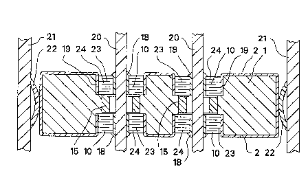
Figure 1 i5 a cross-sectional view of a planar filter array according to a
preferrsd embodimant of the invention. The planar filter array of Fi~ure 1 includes
a substrate or circuit bnard 1. Substrate 1 is preferably made of a high-strsn3~h
crystalline metal oxide material such as alumina, al~hough similar high-strengthrnetal oxide materials may be subs~ituted. The aiumina substrate replaces
conventional filter supports and is arranged as follows:
Exterior surfacas of substrats 1 include a conductiva cornmon e~ternal
ground electrode 2 which may be in the form of discrete tracss or a uniform
coating or layer on the outside of the substrate. In either case, any conven~ional
coating, plating, or trace-applying techniqua ma~jr be used to apply the ground
coating. When placed in a conn~ctor shell 21, comrnon ground electrode 2 may be
connected ~hereto by any sui~able means, numerous ones of which are known, for
example by electrically conductive springs 22.
Provided in substrata 1 are a plurality of cylindrical ceun~er bores 3 and 4
each of which communicates with a cylindrical central connecting bore 5
connecting the coun~er bores on each ~ide of the substrate. Connacting bores 5
are preferably narrower than counter bores 3 and 4 to form annular shoulder~ 6,
as will be described in more d~tail below. External common ground eiectrode 2
may extend into counterbores 3 and 4, but i~ may be also applied solely to tbe
principal external surfaces of the substrate before formin~ coun~erbores 3 and 4.
' ' ' ' ' . ' ',:
' : .
.

2 ~
It will of course be appreciated that bor0s 3-5 nead not n~c~ssarily be cylindrical
in shape, but rather may have any shape necessary to accommodate the shape of
the filter elements to be inserted into the bores.
As shown in Figure 3a, the capacitors 10 provided in counterbores 3 and
are preferably discoidal capacitors, although other filter elements may be
substituted. Each capaci~or 10 includes an annular dielectric body 11 having a
central bore 12, a circumferential ground electrode 14 for connection with common
external ground electrode 2, and an inner hot or live electrode 13 to be electrically
connectsd wi~h one o~ pin contacts 20. Capacitance is establish~d by interleavedelectrodes 23 and 24 provided in the dielectric body and extending alternately from
the ground and hot electrode~. Becausa the capacitors are discrete units, their
capacitance values need not all be ~he same, bu~ rathr~r may easily be varied ifdesired.
The pi filter inductors 15 each consist of an annular ferrite b~ad 16
although, again, other monoiithic filter elements may be substituted. Ferrite bead
16 includes a central bore 17 through which the pin contac~s 20 are inserted.
Ferrite beads 15 fit within bores 5 as discussed above.
In order to assemble the filter array of the ,nreferred embodiment, ferrite
bead 15 is first inserted into bore 5 and secured to the substrate by a suitableadhesive or other supporting means. The discoidal capacitors 10 are then inserted
into respectivs counter bores 3 and 4 from opposite sides of tha substrate to
sandwich ~he ferrite bead. The discoidal capaciturs rest on annular shoulders and
are preferably soldered, as indicated by reference numaral 19, to common external
'

ground 2 in order to establish elactrical connection betwean the common ground
alectrode and the ground electrodes 14 of the capaci~ors. Although soldering is
preferred, other rneans of securing the discoidal capacitors in the counter bores,
such as use of electrically conductive adhesive or a conductive retention spring may
be substituted.
The final step in the assembly procass is simply to insert pin contacts 20
through bores 12 and 17 of the respective capacitors and the ferrite beads and to
electrically connect the pins to the hot electrodas 13 of tha capacitors by soldering,
as indicated by reference numeral 18, or by use of a suitable adhesiw or reten~ion
1 0 spring.
It wili of course be appreciated by those skilled in the art that the monolithicsubstrate and pi filter arrangement may be modified within the scope of the
invention to include a variety of different fil~er structures. Discoidal filter elements
other than capacitors, for example, may be substitu~ed for one or more of the
capacitors used in the preferred embodiment. In addi~ion, one or more of the ferrite
beads may be omitted and/or replaced by other filter elemeflts. The filter substrate
itself may be used in a variety of different connec~or configurations, so long as
some means is provided to establish ~n electrical connection between the
connector shell and the common extarnai ~round 2 on the substrate.
Numerous othar variations of the invention will undoubtedly occur to ~hose
skilled in the art and, therefore, i~ is intended that the invention not be limited to
the specific smbodiment discussed above, but rather that it be definsd solely by the
appended claims.
.

Dessin représentatif
Une figure unique qui représente un dessin illustrant l'invention.
États administratifs

2024-08-01 : Dans le cadre de la transition vers les Brevets de nouvelle génération (BNG), la base de données sur les brevets canadiens (BDBC) contient désormais un Historique d'événement plus détaillé, qui reproduit le Journal des événements de notre nouvelle solution interne.

Veuillez noter que les événements débutant par « Inactive : » se réfèrent à des événements qui ne sont plus utilisés dans notre nouvelle solution interne.

Pour une meilleure compréhension de l'état de la demande ou brevet qui figure sur cette page, la rubrique Mise en garde , et les descriptions de Brevet , Historique d'événement , Taxes périodiques et Historique des paiements devraient être consultées.

Historique d'événement

Description Date
Inactive : CIB de MCD 2006-03-11
Le délai pour l'annulation est expiré 1994-09-27
Demande non rétablie avant l'échéance 1994-09-27
Réputée abandonnée - omission de répondre à un avis sur les taxes pour le maintien en état 1994-03-28
Inactive : Demande ad hoc documentée 1994-03-28
Demande publiée (accessible au public) 1992-10-02

Historique d'abandonnement

Date d'abandonnement Raison Date de rétablissement
1994-03-28
Titulaires au dossier

Les titulaires actuels et antérieures au dossier sont affichés en ordre alphabétique.

Titulaires actuels au dossier
AMPHENOL CORPORATION
Titulaires antérieures au dossier
EDWARD R., JR. GLIHA
Les propriétaires antérieurs qui ne figurent pas dans la liste des « Propriétaires au dossier » apparaîtront dans d'autres documents au dossier.
Documents

Pour visionner les fichiers sélectionnés, entrer le code reCAPTCHA :


Pour visualiser une image, cliquer sur un lien dans la colonne description du document. Pour télécharger l'image (les images), cliquer l'une ou plusieurs cases à cocher dans la première colonne et ensuite cliquer sur le bouton "Télécharger sélection en format PDF (archive Zip)" ou le bouton "Télécharger sélection (en un fichier PDF fusionné)".

Liste des documents de brevet publiés et non publiés sur la BDBC .

Si vous avez des difficultés à accéder au contenu, veuillez communiquer avec le Centre de services à la clientèle au 1-866-997-1936, ou envoyer un courriel au Centre de service à la clientèle de l'OPIC.


Description du
Document 
Date
(aaaa-mm-jj) 
Nombre de pages   Taille de l'image (Ko) 
Dessins 1992-10-01 2 50
Abrégé 1992-10-01 1 14
Revendications 1992-10-01 5 142
Description 1992-10-01 6 203
Dessin représentatif 1999-07-08 1 20
Courtoisie - Lettre du bureau 1992-10-06 1 49