Note : Les descriptions sont présentées dans la langue officielle dans laquelle elles ont été soumises.
2061273
Specification
Title of the Invention
Improved process for preparing a layered structure containing at least
one thin film of oxide superconductor
Back~round of the Invention
Field of the Tnvention
The presel1t invel1tiol1 relates to improvement in a process for
preparing a layered structllle containing at least one thin film of oxide
superconductor, more palticulally, it relates to a process for cleaning a
surface of a bottom supelcol1ductor layer.
In first preferred embodiment, the process is used for depositing
more than one thil1 film of oxide superconductor each possessing a
different crystal orientcltiol1 successively on a substrate.
In second prefelle(l embodiment, the process is used for depositing
a top superconducting layer on a bottom superconductor layer.
Descliptiol1 of the related art
Oxide superconductols are expected to be used in a variety of
applications due to theil higl1el critical temperatures than conventional
metal superconductors. ln tact, Y-Ba-Cu-O oxide superconductor possess
the critical temperatule above ~0 K and Bi-Sr-Ca-Cu-O and T1-Ba-Ca-
Cu-O oxide supercol1ductols possess that of above l00 K.
7 ~
'_.
These oxide sllperconductors, however, possess crystal anisotropy
in their superconducting properties. In fact, the highest critical current
density is observed in a direction which is perpendicular to c-axis of their
crystal. From this fact. the direction of crystal must be considered in
5 actual utilization of these oxide superconductors.
When the oxide superconductors are used in superconducting
electronics such as superconducting devices or integrated superconducting
circuits, it is indispensable to prepare at least one thin film of the oxide
superconductors. The problem of crystal anisotropy becomes much
10 severe in such thil1 film~ of oxide superconductors. For instance, in
order to realize higl1-pelfoll11al1ce superconducting devices or integrated
superconducting circllit~. it is requested to prepare two kinds of
superconducting wiril1g lines: one part in which electric current flows in
parallel with a surface of substrate and another part in which electric
15 current flows pelpendiclllally to the surface of substrate. For example,
in superconductil1g electrodes. current flows in parallel with the surface
of substrate while~ ill intellayer connecting superconducting wiring lines
which connect layer s stratified on the substrate, current flows
perpendicularly to the sllrrace of substrate. Therefor, when oxide
20 superconductor is u.sed in hi~h-perforrnance superconducting devices or
integrated supercond-lctil1~ circuits, it is requested to deposit both of c-
axis orientated thin filn1 of o~ide superconductor in which the critical
current density along the direction which is in parallel with the surface of
substrate is l1igher tl1al1 the otl1er directions and of a-axis (or b-axis)
2 5 orientated thin film of oxide ~uperconductor in which the critical current
density along the direction wl1ich is perpendicular to the surface of
substrate is hi~her than the c-axis orientated thin film on a common
20~273
.....
surface of a sub.strate. llereil1after, only a-axis oriented thin film is
referred, since electric cullel1t flows equally along the direction which is
perpendicular to the surface of substrate in a-axis orientated thin film and
in b-axis orientated thin film.
In the multi-layered structures for the superconducting devices or
integrated superconducting circuits, two layers of a c-axis oriented thin
film of oxide superconductor and of an a-axis oriented thin film of oxide
superconductor must be deposited successively. Crystal orientation of the
thin film of oxide supelcollductol can be controlled by selecting or
adjusting film-formil1g temperature which is determined by substrate
temperature. In fact, the a-axis oriel1ted thin film can be realized at a
substrate temperature whicl1 is lower by about SO to 100 ~C than a
substrate temperatllre at whicl1 the c-axis oriented thin film grows.
In a supelconductil1g jul1ction of so-called Josephson Junction
realized with oxide supelcol1dLlctor~ it is requested to deposit a bottom
superconductor layer, an intermediate thin film of non-superconductor
and a top superconductor layer on a substrate successively.
Josephson elemel1t is a two-terminals element, so that a logical
circuit consisting of Josephsol1 elements alone becomes complicated. In
order to overcome this demelit of complexity, a variety of ideas of three-
terminals elements are proposed. Tn the superconductor transistors
consisting of supercol1d-lctol and semiconductor which is a typical three-
terminals elemel1t, it is also required to combine a thin film of
semiconductor wit]1 a thil1 film of oxide superconductor and hence
successive deposition ot' thil1 films each made of different material is
required.
_ _ J _ _
206~273
.... ..
Successive deposition of a thin film of ordinary conductor such as
metal on a thill film of oxide superconductor is required also in the other
type superconducting elemellt consisting of superconductor and ordinary
conductor. In these superconducting elements, a superconducting current
5 passes through a thin film of non-superconductor sandwiched between
two layers of superconductors positioned close to each other. A distance
between the two adjacent superconductors is determined by the coherence
length of superconductor. Since the coherence length of oxide
superconductors is very short, the distance between two adjacent
10 superconductors li1USt be ~everal nanometer.
In addition to this, frol11 a point of view as performance of the
superconducting devices, all thil1 films in the superconducting device
must have higl1 crystallil1ity, in other words, these thin films are
preferably made of a sil1gle crystal or polycrystal having crystal
15 orientation whicl1 is sil11ilal to sil1gle crystal. When the superconducting
device has thin film(s) made of polycrystal whose crystal orientation is
not well-ordered or has amolpl1ous thin film(s), high-performance of the
superconducting device cal- l10t be expected and hence function thereof
When more thal1 two thil1 films are deposited successively on a
20 common substrate, it is usucll practice to subject a surface of a bottom
superconductor layel to cleanil1g operation before a top superconductor
layer is deposited, othelwise electrical continuity between the bottom
superconductor layer alld the top superconductor layer is spoiled due to
contaminants adsorbed on a ~ulfclce of the bottom superconductor layer
25 or undesirable oxides produced on the surface. Discontinuity of two
layers result in formatioll of a undesirable junction between two layers.
Superconducting devices or integrated superconducting circuits having
206427~
such undesirable junctio n do not show desired performance and
sometimes do not work.
In particular, the surface condition of the bottom superconductor
layer should be considered carefully because the coherence length of
oxide superconductors is very short. Still more, oxygen of oxide
superconductors is rather unstable and easily escape out of the thin film.
Excessive oxygen deficient result in deterioration of superconducting
properties and, in the worst case. loss of superconductivity.
Therefole, the sulf~lce of bottom superconductor layer must be
clean and also m~lst hclve well-ordered crystallinity or superconducting
property.
In the field of semicol1ductor industries, the surface of bottom
superconductor layer is often cleaned with ultra-pure water, by chemical
washing, dry or wet etcl1ing or the like. In the case of oxide
superconductors, however, these clearing technique can not be used due
to high reactivity of oxide superconductors. Tf the surface of thin film of
oxide supercond~ctor is treated by these known techniques, undesirable
reaction occur on the sulface? resultil1g in that cleanness of the surface
become worse and crystallil1ity and superconducting property are lost.
It is also knowl1 to deposit the top superconductor layer, just after
the bottom supercol1dLIctol layer of oxide superconductor has been
deposited, in an identical appalatus. This technique, however, requires a
big apparatus and matelials to be used for the top superconductor layer
are limited.
An object of the presellt invelltion is to solve the problems and to
provide an improved process for preparing a layered structure
containing at lea~st one thil1 film of oxide superconductor without
2 ~t ~
.._
deteriorating supercol~ lctillg properties of the thin film of oxide
superconductor.
Another object of the present invention is to provide an improved
process for depositing more than one thin film of oxide superconductor
5 each possessing a different crystal orientation successively on a substrate.
Still another object of the present invention is to provide an
improved process for depositing, on a thin film of oxide superconductor,
another thin film of differellt material.
Sul~ ry of the Invention
The present invention provides a process for producing a layered
structure on a first film of oxide superconductor deposited on a substrate
and having a contaminated surface, characterized in that said first film of
oxide superconductor is heat-treated in an atmosphere containing oxygen
having a purity higher than 5 N (99.999 %) under a background of ultra-
high vacuum of lower than 1 x 10⁻⁹ Torr, wherein a partial pressure of
oxygen is between 20 mTorr and 25 Torr, said heat-treatment being
conducted at a temperature between 350~C and 700~C, and then another thin
film is deposited on said first film of oxide superconductor.
2 ~ The essence of the process according to the present invention resides
in that a surface of a botlom superconductor layer is heat-treated in
oxygen of high purity so as to clean the surface before another thin film
is deposited tllereoll.
The heat-treatmellt is eftected just before the top superconductor
layer of oxide supercond-lctor is deposited on the bottom superconductor
layer so that contaminallts such as hydrocarbons or metal carbides
'~ 7~ 7 ~
adsorbed or deposited on tl-e surt'ace of the bottom superconductor layer
are removed by ~he hea~-tleatl11ent. The heat-treatment permit to repair
local surface disorder of crystallinity in the bottom superconductor layer
and to supply enough oxygen by the heat-treatment so that
5 superconducting property is improved.
Oxygen of high-purity used in the process of the present invention
contains substantially no H20 and CO2 and reacts easily with and
deteriorates the oxide superconductor.
The heat-treatmel1t i~ effected at a heating temperature between 350
1 0 and 700 ~C for a thil1 film of Yl Ba~Cu3O7 x. If the heating temperature
is not higher than ~0 ~C. the recrystallized surface of thin film can not
be repaired and,. if the heatil1g temperature exceed 700 ~C, order of
crystal of the thil1 film of oxide superconductor is disturbed. Time
duration of the heat-treatmel1t depend on the partial pressure of oxygen
15 and the heating tempelatule.is usually between several minutes and
several hours.
The substrate is prefelably a single crystal of oxide such as MgO,
StTiO3, PrGaO~ or the lilie.
The thin fi lm of oxide superconductor can be a bottom
20 superconductor layer which is deposited directly on a surface of the
substrate. This bottom supercol1ductor layer can be a thin film of oxide
206427~
, .~.
. ~
superconductor, for exal11ple, a c-axis oriented thin film of
YlBa2Cu307 x.
The process according to the present invention is applicable to any
known oxide superconductors and is advantageously applicable to Y-Ba-
Cu-O oxide superconductor, Bi-Sr-Ca-Cu-O oxide superconductor and
Tl-Ba-Ca-Cu-O oxide superconductor which have the most attractive
properties including their high critical temperatures.
First Embodiment
In a preferled firsl embodil11ent of the present invention, another
thin film is made of oxide superconductor which may be made of the
same material as or differel1t material from the bottom superconductor
làyer. In this case, anotl1el thil1 film can be an a-a~is oriented thin film
of Y l Ba2Cu3O7 x .
Namely, in the fir~t embodin1ent~ the present invention provides a
process for depositing a first thil1 fihn of an oxide superconductor and a
second thin film of oxide supercol1ductor successively, crystal orientation
of the first thill film being differel1t from that of the second thin film,
and the first thin film havil1g a contan1il1ated surface, characterized in
that the contamil1ated s~llface of the first thin film is heated in an
atmosphere contail1il1g oxygel1 of hi~h purity at a temperature between
an evaporation tempelatllle of contaminants and a film forming
temperature of the first thil1 film before second thin film is deposited.
2 5 In the first embodimel1t, tlle process according to the present
invention is applicable tOr lamil1atil1g or stratifying thin films of oxide
superconductor each havil1g a different crystal orientation successively
206g273
and, more particularly~ is adval1tageously applicable for depositing an a-
axis oriented thin film of oxide superconductor on a c-axis orierited thin
film of oxide superconductol.
5 Second Embodiment
In a preferred second embodiment of the present invention, the
present invention provides a process for depositing, on a first thin film
of oxide superconductol wl1o~se surface is contaminated, a second thin
film made of dift'erent material from the oxide superconductor,
10 characterized in that the finst tl1in film of oxide superconductor is heated
in an atmosphere contail-il1g oxygen of high purity at a temperature
between an evaporation temperature of contaminants and a film forming
temperature of the first thil1 film before the second thin film is deposited.
In this case, the second thil1 film can be made of non-superconductor, for
15 example insulator ~sucl1 as MgO or metal such as Ag. A third thin film of
oxide superconductol- can he deposit additionally on the second thin film.
The second emboclil11el1t of the process according to the present
invention is applicable for depositing, on a thin film of oxide
superconductor, a thin film of in~sulator or ordinary conductor in order
2 0 to fabricate supel cond~lctil1g devices.
In botll embodil11el~t~s~ tlle process according to the present
invention is applicable. for example, to such a thin film of oxide
superconductor which is exposed to air and hence whose surface is
deteriorated, in order to clean the surface before another thin fil~n or top
25 superconductor layer having a differel1t crystal orientation or of different
material is depo~sitecl thelec)l1~ .so that more than two thin film layers each
having a different crystal oriel~tcltiol1 or a combination of a thin film of
2U6~273
oxide superconductol ancl a noll-superconductol can be deposited in
different film forming apparatuses independently at their optimum
conditions and hence the resulting layered thin films show an improved
superconducting property.
In conclusion, the present invention provides a process for
stratifying more than one thill film of oxide superconductor each having
different orientation without spoiling superconducting property. The
process according to the presellt invelltion also permits to deposit, on a
thin film of oxide supelcollductol, another thin film of different material
without spoilin~ supelcoll(luctillg property. The obtained stratified thin
films show improved crys~allillity and improved contilluity or matching
in lattice constallts at theil intelface which are re4uested for realizing
superconducting elemellts or integlated superconducting circuits from
which high-perforlllallce sllpelcollducting devices are fabricated.
1 5
Brief l)escliption of the Drawing
Fig. I illustlates succes~sive steps for preparing a layered structure
containing at least one thill film of oxide superconductor by the process
according to the present invelltion.
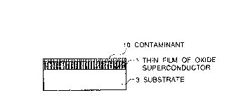
Fig. IA sllows a substlate 3 on wllich thin films àre to be deposited
successively by the process accolclillg to the present invention.
At first, a tllin film ol' oxide superconductor (I) is deposited on the
substrate (3) by off-axis sputtering method, laser abrasion method,
reaction evaporation method? MBE or CVD technique. After deposition
complete, tlle substrate (3) havillg the deposited thin film of oxide
superconductor (I ) is taken out of a sputtering chamber. In air, a surface
-- 10 --
2064273
of the thin film of oxide supelconductor (]) reacts with moisture to
produce a deteriorated portion (10) thereon and is contaminated with
hydrocarbons, BaC03, BaCuO2 or the like as is shown in Fig. lI3.
Then, the substrate (3) is placed in a ultra-high vacuum chamber
5 which is then vacuumed lower than 1 x 10⁻⁹ Torr. After that, the thin
film of oxide superconductor (1) is heat-teated under suitable operational
conditions. The surface of the thin film of oxide superconductor (1) is
monitored by a quadropole mass spectrometer (QMS) and is analyzed by
means of a low enelgy electroll diffraction analyzer (LEED) or a X-ray
10 photoelectron spectrometer (XPS) after the heat-treatment, in such a
manner that contalllillal-ts are removed, deteriorated portion (10)
disappears and a çrystallille s~lrface is exposed.
On the resulting cleaned surface (Fig. lC), another thin film (2)
(oxide superconductol or different material) is deposited in the same
15 chamber by off-axis sp~lttelillg metllod, laser abrasion method, reaction
evaporation method MBE~ CVD techllique or the like.
Description of the Preferred Embodiment
Now, the presellt invelltioll will be described with refe;rring to
2 0 Example but the scope of the inventioll should not be limited thereto.
Example 1
In this Example 17 all a-axis oriented thin film of oxide
superconductor of Yl Ba2Cu3O7 x was deposited on a c-axis oriented thin
25 film of oxide supelcolld-lctor of YlBa2Cu3O7 x by the process according
to the present invelltioll whose steps are illustrated in Fig. 1.
I I
7 ~
"_
At first, a c-axis oriellted thin film of oxide superconductor of
YlBa2Cu3O7 x (1) havillg a thicklless of 300 nm is deposited on a
substrate (3) of MgO ( I ()()) by off-axis sputtering method under
following operational conditions:
Sputtering gas Ar : 90 % by volume
~2 : 10 % by volume
Pressure : 10 Pa
Substrate temperature : 700~C
After deposition complete, the substrate (3) is taken out of a
10 sputtering chambel. A surface of the resulting thin film of oxide
superconductor (l ) has a deteriorated portion (10) thereon and is
contaminated with hydrocarbons BaCO3, BaCuO2 or the like produced
by a reaction witll moistule in air.
Then, the substrate (~) is placed in a ultra-high vacuum chamber
15 which is then vacuumed lower tllan I x l0-9 Torr.
After that, the thill film of oxide superconductor (I) is heat-teated
under following operatiol-al conditions:
Atmosphel-e : ~2 (purity of more than SN,
partial pressure of 25 Torr)
Heating temperatllle : 600 ~C (substrate temperature)
Heatingtime : 10 min (after then, quenched in
oxygen atmosphere)
The surface of the thin film of oxide superconductor (1) is monitored by
a quadropole mass spectrometer (QMS) and is analyzed by means of a
2 5 low energy electroll diffraction analyzer (LEED) or a X-ray
photoelectron spectrometer (XPS) in order to confirm that contaminants
4 ~
.,.._,i
or deteriorated portion (10) ale removed and disappear and a crystalline
surface is exposed:
On the resulting cleaned surface (Fig. lC), an a-axis oriented thin
film of oxide superconductor of YIBa2Cu3o7-x (2) having a thickness of
5 200 nm is deposited by off-axis sputtering method under following
operational conditions:
Sputtering gas A r : 90 % by volume
O~ : 10 % by volume
Pressure : 10 Pa
Substrate temperat-lre : 60() to 650 ~C
In the layered thill films prepared by this Example 1, it is
confirmed that both of the bottom superconductor layer and the top
superconductor layer pos~sess imploved crystallinity and show continuity
at an interface betweell thelll.
1 5
Example 2
Example 1 is repeated except that a thin film of MgO of the same
thickne~s is deposited 011 the c-axis oriented thin film of oxide
superconductor of YlBa2Cu3O7 x in place of the a-axis oriented thin film
2 0 of oxide superconductol of Y I ~a~Cu3O7 x.
In this Example 2, a thill film of MgO (2) having a thickness of 200
nm is deposited by evaporation method under following operational
conditions:
Pressure : 10 Pa
Substrate temperatllle : 200~C
In the layered thill fi Ims prepared by Example 2 also, it is
confirmed that both of the bottom superconductor layer and the top
-,~,
k- ~
206~273
superconductor layer possess improved crystallinity and show a sharp
boundary at their intelface.
Example 3
Example 2 is repeated except that the thin film of MgO is replaced
by a thin film of Ag of the same thickness.
The thin film of Ag having a thickness of 200 nm is deposited by
evaporation method under following operational conditions:
Pressure : 10 Pa
Substrate temperature : 200 ~C
In the layered thill films prepared by Example 3 also, it is
confirmed that both of the bottom superconductor layer and the top
superconductor !ayer possess improved crystallinity and show good
contact between two materials.
---- I 4 ----