Note : Les descriptions sont présentées dans la langue officielle dans laquelle elles ont été soumises.
PATENT
26948-353
- 1 -
BROADHAND PHASE SHIFTER AND VECTOR MODULATOR
FIELD OF THE INVENTION
This invention relates to analog phase shifters and
vector modulators, and in particular to a broadband
frequency vector modulator for accurately shifting the
phase of an input periodic signal by any angle between 0°
and 360°.
~a~~~~
- 2 -
BACKGROUND OF THE INVENTION
As is well known, a periodic signal has a frequency,
a magnitude and a phase. When analyzing periodic signals,
the amplitude and phase of the signal is, for mathematical
convenience, represented by a phase vector, called a
phasor, that rotates about an origin. The angle of the
phasor with respect to a reference indicates the phase of
a signal at a particular time, and its length or magnitude
indicates the amplitude of the signal. In view of this
phasor representation, periodic signals are often spoken
of in the art as "vectors," and the process of phase
shifting periodic signals is commonly referred to as
"vector modulation". In the following description, as in
the art, the term "vector" refers both to actual periodic
signals as well as to an abstract mathematical
representation of periodic signals.
Vector analysis of periodic signals demonstrates
several concepts important to understanding the present
invention. When, for example, two or more signals are
summed, the amplitude and phase of the resulting signal may
be determined by adding the vectors of the phasors of each
signal. This vector representation of summed signals thus
suggests a common method of vector modulation or phase
- 3 -
shifting referred to as a variable amplitude phasor
approach. In this approach, an output signal having a
given phase shift may be generated by properly splitting
and shifting the input signal and summing the two resulting
split signals. For example, equally splitting an input
signal into two identical signals, shifting one by 90° and
the other by 180°, and adding the two delayed signals
produces the input signal phase shifted by 135°. In this
example, by varying the amplitude of one of the signals,
thereby varying the length (magnitude) of its vector
representation, the input signal can be phase shifted
through all the angles between 90° and 180°.
Although phase shifters and vector modulators have
a wide range of uses, one important use is in steering a
beam of phased array antenna. A phased array antenna is
comprised of a plurality of antenna elements, each of which
receives signals identical in almost every respect except
for their phases. A phased array antenna generates a beam
in a given direction by constructively combining radiation
emitted from each individual antenna element. To steer the
beam, the phases of the signals applied to each element are
appropriately shifted by phase shifters. Accurately
pointing the beam and, at the same time, suppressing
c,
- 4 -
radiation sidelobes depends on accurately controlling the
phase shifts between antenna elements.
In a paper entitled "A Monolithic 10-GHz Vector
Modulator", published by the IEEE in 1983 as part of its
GaAs IC Symposium, Eric W. Strid describes a phase
controller (hereinafter referred to as the "Strid vector
modulator") that is monolithically implemented as a single
integrated circuit utilizing the variable amplitude phasor
approach. This single integrated circuit is small and
light, and therefore has the advantage of being usable with
phased array antennas on moving platforms such as military
aircraft and spacecraft.
The circuit of the Strid vector modulator includes
a first and a second tapped lumped delay line. The delay
lines are like those used by a transversal filter for
matched filter detection of PCM signals. The periodic
signal to be selectively phase shifted is applied to an
input of one of the delay lines. Each delay line is
comprised of a number of series connected signal delayers
to generate phase shifts. The amount of delay between each
signal delayer in the delay lines is chosen such that the
phase of a periodic signal at a center frequency in the
band of interest is delayed by 90 ° or 120 ° for each delayer
- 5 -
as the signal propagates through each delay line. A
plurality of field effect transistors (FETs), connect each
delayer of the first delay line to a corresponding delayer
on the second delay line.
The paths through the delay elements and the FETs
form a number of vector channels. Each vector channel
provides to the outputs of the Strid vector modulator
variably phase shifted versions of the input signal for
summing. The signal generated by each vector channel
differs in phase by a predetermined amount, usually in
increments of 90° or 120°. By turning the FETs "on" and
"off" and adjusting the amplitude of the applied voltage
to each FET, different vectors of differing magnitudes and
phases may be created and added to vary and control the
phase shift of the input signal. Therefore, the Strid
vector modulator functions as an analog phase shifter
capable of producing any angle between 0° and 360°.
The Strid vector modulator satisfies many
requirements for phase shifters used for phased array
antennas aboard moving platforms, namely that the vector
modulators be small and light, and consume little power.
However, the vector modulation bandwidth of the Strid
vector modulator is severely narrow, especially for signals
- 6 -
in the microwave range, as a result of the utilization of
signal delayers for creating phase shifts.
At a given center frequency the vectors of the
periodic signal in each of the four vector channels are
separated by the required 90° of phase shift. However, use
of frequency dependant signal delayers to generate phase
shifts results in different transit times through the
vector channels for different frequencies of the input
signal. Thus, deviations in the input frequency causes
skewing of the frequency versus phase response of the Strid
vector modulator resulting in phase distortion in the
output signal. As the frequency of the input periodic
signal applied to a Strid vector phase modulator deviates
from the center frequency, the angles between the vectors
of the signal samples begin to deviate and drift
substantially and are no longer fixed at 90° apart.
When used in conjunction with phased array antennas,
the Strid vector modulator introduces intolerable phase
errors and distortions in the signal that seriously effect
array beam pointing accuracy and the suppression of array
side lobe radiation. The Strid phase shifter is,
therefore, unsuitable for use in highly accurate phased
array antennas transmitting broadband periodic signals.
It is theoretically possible to correct the Strid
phase errors and distortions by varying the applied FET
voltage as the frequency of the vector modulator input
signal changes. However, aside from the impracticality of
dynamically adjusting the amplification of the FETs as a
function of input signal frequency variation, the extra
circuitry and complexity required to provide adjustable FET
amplification to correct the resulting phase distortions
of the Strid device leads away from the goals of a small,
simple, low power device capable of monolithic
implementation to achieve reproducible performance and mass
production.
Accordingly, there is a need for a small, simple,
low power vector modulator having consistent broadband
frequency response further capable of being implemented on
a monolithic chip.
BRIEF DESCRIPTION OF THE INVENTION
The present invention is an improvement of the
Strid analog vector modulator. It is, unlike Strid, truly
broadband, sweeping all angles from 0° to 360° over broad
bandwidths of the input periodic signal without severe
phase distortion, especially in the microwave frequency
range. Yet, the broadband phase shifter of the present
invention preserves many of the advantages offered by the
Strid vector modulator, including simple circuitry and
small size, even at low frequencies, and possible
monolithic implementation advantages such as even smaller
size, lightweight packaging, mass production and
reproducible performance.
In place of the parallel lumped delay lines of
the Strid vector modulator, the invention utilizes a first
and second parallel artificial transmission line coupled by
field effect transistors (FETs). The first artificial
transmission line is comprised of low pass filters
connected in series, each low pass filter retarding the
phase or vector of an input signal by minus 45°. The
second artificial transmission line is comprised of high
pass filters connected in series, each high pass filter
advancing the vector of the sampled input signal by 45°
- 9 -
Like the Strid vector modulator, vector generating channels
are established by turning "on" and "off" the FETs
interconnecting the low pass and high pass filters so as
to generate vectors having angles of 0°, 90°, 180° and
270°.
Unlike the Strid vector modulator however, where
the lumped delay lines introduced different transit times
through each vector channel, the low pass and high pass
filters utilized by the present invention on, respectively,
the gates and drains of the FETs equalize path lengths and
transit times through each vector generating channel with
variations in frequency of the input periodic signal. The
bandwidth of the device is therefore limited only by the
roll-off frequency characteristics of the filters, rather
than by the narrow band frequency response characteristic
of signal delayers. Vectors generated by the present
invention therefore have a relatively flat phase versus
frequency response over a broad bandwidth, the vectors
remaining spaced apart by 90°.
Furthermore, the invention takes advantage of the
parasitic capacitance associated with the gates of the FETs
by incorporating that capacitance into each low pass filter
structure on the first artificial transmission line. The
-to-
number of components and complexity of the filter are
thereby reduced. In addition, utilization of artificial
transmission lines for the vector modulator in accordance
with the present invention has better than a 20 dB return
loss over a broad bandwidth.
In accordance with one aspect of the present invention
there is provided an analog phase shifter for shifting the
phase of an input periodic signal by any selected angle
between 0° and 360° comprising: a first artificial
transmission line having a plurality of substantially
matched low pass filter sections connected in series, each
low pass filter section shifting the phase of a signal on
the first artificial transmission line by a predetermined
amount, an end of the first artificial transmission line
terminating as an input port for the input periodic signal;
a second artificial transmission line having a plurality of
substantially matched high pass filter sections connected
in series, each high pass filter section shifting the phase
of a signal on the second artificial transmission line by
a predetermined amount, an end of the second artificial
transmission line terminating as an output port for a
phase-shifted version of the input periodic signal; a
transistor corresponding to each pair of low pass and high
pass filter sections, each said transistor having a first
electrode coupled to the corresponding low pass filter
section and a second electrode coupled to the corresponding
high pass filter section; and bias means coupled to each
transistor for individually adjusting the conductivity of
W~~ ~'
- l0a -
each transistor to provide a selected angle of phase shift
at each transistor for the input signal.
In accordance with another aspect of the present
invention there is provided an analog phase shifter and
vector modulator for shifting a phase of an input signal by
any angle from 0° to 360° comprising: an input port for
receiving the input signal at a first phase, the phase of
the input signal to be shifted by a preselected angle; a
plurality of transistors, each transistor having a gate and
a drain; a first plurality of inductors individually
connecting the gate of one transistor to the gate of an
electrically adjacent transistor of the plurality of
transistors and an inductor connecting the input port to
the gate of a first one of the transistors; an output port;
a plurality of capacitors individually connecting the drain
of one transistor to the drain of an electrically adjacent
transistor of the plurality of transistors and a capacitor
connecting the output port to the drain of a last one of
the transistors; and a second plurality of inductors
individually coupling the drain of each transistor to a
ground; and bias means connected to each of the plurality
of transistors for individually adjusting the conductivity
of a transistor to shift the phase of the input signal at
each transistor.
In accordance with yet another aspect of the present
invention there is provided an analog vector modulator,
comprising: an input port for receiving a signal to be
phase shifted; a first plurality of inductors series
- 1 o b - ~ ;
connected at a plurality of first filter taps, the first
plurality of inductors connecting the input port to a first
terminating resistance; an output port for providing a
phase shifted version of the signal received at the input
port; a plurality of capacitors series connected at a
plurality of second filter taps, the plurality of
capacitors connecting the output port to a second
terminating resistance; a plurality of transistors each
having a first electrode including a parasitic capacitance
coupled to one of the plurality of first filter taps and a
second electrode coupled to a corresponding one of the
plurality of second filter taps; a plurality of bias means
each providing a variable bias voltage applied to one of
the plurality of transistors to vary the conductivity of
the transistor and alter the phase of the input signal at
the output port.
_ m _
BRIEF DESCRIPTION OF THE DRAWINGS
A more complete understanding of the present
invention and its advantages may be had by reference to the
foregoing Background of the Invention and the following
Detailed Description, both taken in conjunction with the
accompanying Drawings wherein:
FIGURE 1 is a schematic diagram of a prior art
Strid vector modulator;
FIGURE 2 is a vector phase angle versus frequency
plot of the operating characteristics of the prior art
Strid vector modulator shown in FIGURE 1;
FIGURE 3 is a schematic diagram of a vector
modulator in accordance with the teachings of the
invention;
FIGURES 4A and 4B are schematic circuit diagrams
for the low pass and high pass filter sections of the
vector modulator shown in FIGURE 3;
FIGURE 5 illustrates drawings of vectors
generated by the vector modulator of FIGURE 3 in several
modes of operation; and
FIGURE 6 is a vector phase angle versus frequency
plot of the operating characteristics of the vector
modulator of the present invention as shown in FIGURE 3.
- 12 -
DETAILED DESCRIPTION OF THE DRAWINGS
Referring now to FIGURE 1, there is shown a
schematic diagram of the prior art Strid phase shifting
vector modulator 101. As can be readily seen, the prior
art vector modulator 101 is comprised of a first and second
delay line, 103 and 105 respectively, interconnected by a
number of dual-gate FET transistors 107-110. An input
periodic signal to be phase shifted is received by phase
shifter/vector modulator 101 at input port 111. Input port
111 couples the input signal to one end of a first lumped
delay line 103. The other end of the first lumped delay
line 103 is terminated by a terminating resistance 113.
First delay line 103 is comprised of a number of
individual delays 115 coupled in series and separated by
a number of taps 117. Each tap 117 on first delay line
103 is connected to the second gate 118-121 of the
corresponding dual-gate FET transistor 107-110
respectively. The source 122-125 of each FET is connected
to ground 127.
Second delay line 105 is comprised of a number of
individual delays 129 coupled in series and separated by
a number of taps 131. The signal delay provided by each
delay 115 in the first delay line 103 and each delay 129
- 13 -
in the second delay line 105 is different. Each tap '31
on the second delay line 105 is connected to a drain 13~-
141 of the corresponding FET 107-110 such that taps 131 and
117 share one FET and form a vector channel 142-145.
Precise selection of delay times in each delay line 103 and
105 provide 90° vector separation at the chosen center
frequency of operation. The delayed and phase shifted
signals in each vector channel are summed at the outputs
147 and 149.
In order to control the phase of the signal at the
outputs 147 and 149, the magnitude of the vector generated
in each vector channel 142-145 may be adjusted by
application of a control voltage VA_p to a first gate 150-
153 of each FET 107-110. By properly adjusting the applied
voltage V to each FET and vector channel, a periodic signal
at the output ranging in phase from 0° to 360° can be
theoretically generated.
Referring now to FIGURE 2, there is shown the
frequency response characteristics of the prior art Strid
vector modulator 101 shown in FIGURE 1. In particular,
FIGURE 2 discloses that the Strid prior art modulator has
an extremely narrow bandwidth over which near-90° vector
phase separation is maintained. For example, at a given
- 14 -
center frequency, for example 4.50 GHz, the delays for each
delay line can be precisely chosen to provide exactly 90°
phase shift per vector channel as shown generally at 155.
However, as the frequency of operation drifts away from the
chosen center frequency, the frequency response of the
vector channels becomes severely degraded as generally
indicated at 157 causing each channel to lose its 90° phase
shift. Thus, the Strid modulator is unable, especially in
broadband systems applications, such as phased array
antennas, where precise phase shifting over a wide
frequency range is essential, to maintain accurate phase
control (for steering of the beam) and suppress collateral
phase effects (sidelobe generation).
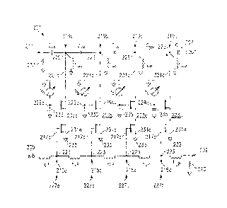
Referring now to FIGURE 3, there is shown a
broadband vector modulator 201 of the present invention.
The vector modulator is generally comprised of a number of
dual-gate or cascade connected MESFETs 203a-203d, an input
port 205, an output port 207 and a low pass and high pass
filter network, 209 and 211 respectively. The MESFETs
203a-203d are coupled to the low pass and high pass filter
networks at a number of taps, 223 and 225.
Input port 205 of the vector modulator 201 is
configured to receive a periodic signal to be phase
- 15 -
shifted. Low pass filter network 209 is coupled to the
input port 205 and is terminated by a terminating
resistance 213. A number of low pass filters 215a-215d
corresponding to each MESFET 203a-203d are coupled in
series between the input port 205 and the terminating
resistance 213 to form the low pass filter network 209
(first artificial transmission line).
As shown in FIGURES 3 and 4A, each low pass
filter 215a-215d is comprised of a "T"-shaped LC low pass
filter circuit having a pair of inductances LLP connected
in series to form the arms of the "T" coupled at tap 223 to
the parasitic capacitance (not shown in FIGURE 3) of the
first gate electrode 217a-217d of each associated MESFET
203a-203d. In forming each LC low pass filter 215a-215d,
two criteria are important.
First, the impedance of the low pass filter network
209 (first artificial transmission line) should match the
characteristic impedance the transmission line coupled to
the input port 205 (generally 50 ohms). Second, each low
pass filter 215a-215d of the low pass filter network 209
should provide a phase shift of minus 180°/N, wherein N is
the number of MESFETs 203 utilized in the vector modulator
201. For example, if four MESFETs are used, as shown in
rr.
- 16 - ~s~~., ,~ ; ,;~ <P
FIGURE 3, each low pass filter 215a-215d should be
configured to provide minus 45° of phase shift.
The equations for the inductances LLP and
parasitic capacitances of the MESFET (CLP, not shown) that
will provide minus 45° of phase shift and match a 50 ohm
transmission line for the low pass filter network 209 are
given below:
LLP = (50*cos (45°) -50) / (w*sin(45°) ) ; and (1)
CLP - 2 * LLP / ( 2 5 0 0 +w2LLP2 ) i ( 2 )
wherein: w is the center frequency of the broadband signal;
and 2500 represents square of the characteristic impedance
(50 ohms) of the transmission line. It will, of course, be
understood that the vector modulator 201 of the present
invention is not limited to a 50 ohm match or minus 45°
phase shift, but may be configured in any other manner
according to equations (1) and (2) above. Incorporation of
the MESFET parasitic capacitance into each low pass filter
215 of the low pass filter network 209 reduces the number
of components in the vector modulator 201, enabling the
modulator to be more efficiently and consistently
manufactured monolithically.
Output port 207 of the vector modulator 201 is
configured to output a phase shifted version of the input
periodic signal. High pass filter network 211 is coupled
- 17 -
to the output port 207 and is terminated by a terminating
resistance 213. A number of high pass filters 219a-219d
corresponding to each MESFET 203a-203d are coupled in
series between the output port 207 and the terminating
resistance 213 to form a second artificial transmission
line.
As shown in FIGURES 3 and 4B, each high pass filter
219a-219d is comprised of a "T"-shaped LC high pass filter
having a pair of capacitances CHP connected in series to
form the arms of the "T" and coupled at tap 225 to a shunt
inductance LHP and the drain electrode 221a-221d of each
associated MESFET. In forming each LC high pass filter
219, the same two criteria of proper impedance match and
phase shift are important.
First, the impedance of the high pass filter network
211 (second artificial transmission line) should match the
characteristic impedance of the transmission line coupled
to the output port 207 (generally 50 ohms). Second, each
high pass filter 219 of the filter network 211 should
provide a phase shift of 180/N°, wherein N is the number
of MESFETs 203a-203d utilized in the vector modulator 201.
For example, if four MESFETs are used, as shown in FIGURE
- 18 -
3, each high pass filter 219 should be configured to
provide 45° of phase shift.
The equations for the capacitances CHP and inductance
LHP that will provide 45° of phase shift and match a 50 ohm
transmission line are given below:
CHP = (cos(45°) + 1)/(50*w*sin(45°); and (3)
LHP = 1250*CHP + 1/ (2*wZCHP) ; (4)
wherein: w is the center frequency of the broadband signal;
and 1250 represents 1/2 the square of the characteristic
impedance (50 ohms) of the transmission line. It will, of
course, be understood that the vector modulator 201 of the
present invention is not limited to a 50 ohm match or 45°
phase shift, but may be configured in any other manner
according to equations (3) and (4) above.
The taps 223 and 225 of each low pass filter section
215a-215d and high pass filter section 219a-219d,
respectively, are coupled through the corresponding MESFET
203a-203d in the vector modulator 201 to form a vector
channel 227a-227d. In the configuration shown in FIGURE
3, each vector channel 227 provides 90° of phase shift from
summing the two 45° phase shifts provided by each included
filter section. The taps for the low pass and high pass
filter sections, 223 and 225 respectively, are coupled to
- 19 - '. '~~ ~'
the first gate electrode 217a-217d and drain electrode
221a-221d respectively of the corresponding MESFET
203a-203d. A second gate electrode 229a-229d of each
MESFET 203a-203d is coupled to a variable DC bias voltage
source Va_d to adjust the amplification of the signal in
each vector channel 227a-227d. The vector modulator 201
circuit is completed by coupling the source electrode
231a-231d to ground 233. Also, a shunt capacitor 235 is
coupled to each second gate electrode 229a-229d.
In the operation of the vector modulator 201, a
signal incident on the input port 205 travels along the low
pass filter network 209 (first artificial transmission
line) toward the terminating resistor 213. The signal is
phase shifted by minus 45° as it passes through each low
pass filter section 215. At each tap 223, the signal is
sampled by the associated MESFET 203. The sampled signal is
selectively amplified according to the applied variable DC
bias voltages Va_d and injected into the tap 225 for the
corresponding high pass filter section 219. At this point
the signal is phase shifted. As the shifted signal
propagates along the high pass filter network 211 (second
artificial transmission line) toward the output port 207,
- 20 -
the signal is added to the shifted signals injected at each
successive tap 225.
The amplified and shifted signals in each vector
channel 227a-227d can be considered to be mathematical
vectors. As shown in FIGURE 5, by selectively turning the
MESFETs 203a-203d "on" and "off" and adjusting the MESFET
bias voltage Va_d, an output signal of any phase from 0° to
360° can be generated.
Referring now to FIGURE 6, there is shown the
frequency response characteristics of the vector modulator
201 of the present invention. Unlike the prior art vector
modulator (see FIGURES 1 and 2), the vector modulator 201
maintains near-90° phase separation in each vector channel
over a wide bandwidth. The use of a combination low pass
and high pass filter networks, 209 and 211 respectively,
rather than delay lines as in the prior art, reduces the
frequency sensitivity because the two filters have nearly
identical roll-off characteristics. Thus, the transit
times traveled by the input signal through each vector
channel are nearly identical over a broad bandwidth. The
bandwidth of the vector modulator is limited only by the
frequency response (roll-off) of each included filter
section rather than by the frequency dependant signal
21 - , ~..~.s ° ;~9 '~ '~
delayers of the prior art. The vector modulator of the
present invention can thus provide a bandwidth of
approximately 30o with a +/- 5° phase error in each vector
channel.
Although a preferred embodiment of the invention
has been illustrated in the accompanying Drawings and
described in the foregoing Detailed Description, it will be
understood that the invention is not limited to the
embodiment disclosed but is capable of numerous
rearrangements and modifications of parts and elements
without departing from the scope of the invention as set
forth in the following claims.