Note : Les descriptions sont présentées dans la langue officielle dans laquelle elles ont été soumises.
2064681
SEMICONDUCTOR LASER DIODE
BACKGROUND OF THE INVENTION
Field of the Invention
This invention relates to a semiconductor laser
diode used for a light source of an optical
communication and, more particularly, to a
semiconductor laser diode which has excellent
temperature characteristics and low threshold current.
Description of the Prior Art
There have been a semiconductor laser diode of
the type for a short wavelength region (~ = 0.78 - 0.89
~m) and a semiconductor laser diode of the type for a
long wavelength region (~ = 1.2 - 1.6 ~m). The
temperature characteristics of a semiconductor laser
diode of the type for the long wavelength region used
mainly for an optical communication are deteriorated as
compared with that for the short wavelength region.
This causes drastic increase of threshold current and
drastic decrease of differential quantum efficiency at
higher temperature.
The threshold current of a laser diode is
represented by an equation (1) as below, where
operating threshold current Ith is a function of a
temperature T in Kelvin, and To denotes characteristic
temperature in Kelvin.
2064681
-
Tth = Itho~exp (T/To) (1)
As understood from the above equation (1), a
semiconductor laser diode having high characteristic
temperature To is excellent due to its stable
temperature characteristics.
In case of an AlGaAs (ternary crystalline solid
solution) short wavelength band semiconductor laser
diode, the characteristic temperature To is usually
larger than 150 K.
On the contrary, in an InGaAsP (quaternary
crystalline solid solution) long wavelength region
semiconductor laser diode, To is as low as 60 K at
temperature region 0C - 40C, and it deteriorates
further at higher temperature region.
Further, in case of a long wavelength region
semiconductor laser diode having an active layer of a
quantum well structure, To = 150 K at lower
temperature region than 40C, but To is as low as 60 K
at higher temperature than 40C.
The dominant reason of the low characteristic
temperature of the long wavelength region semiconductor
laser diode is attributed to the carrier (electron)
overflow from active layer to p-clad layer generated by
Auger recombinations.
(Reference 1. Longwavelength Semiconductor Lasers,
2064681
Agrawal and Outta, Van Nostrand Reinhold Company, N.Y.
pp 71-141.)
In order to prevent such a carrier loss, ~Double
Carrier Confinement (DCC)" hetero junction" has been
proposed, and the following reference 2 is disclosed
with respect to this.
Reference 2: IEEE J. Quantum Electron., Vol.
QE-l9, pp.1319-1327
A representative DCC structure disclosed in the
reference 2 will be described with reference to Fig. 7.
In case of a DCC structure shown in Fig. 7, an
N-type InP clad layer 2, an InGaAsP first active layer
3, a p-type InP intermediate clad layer 4, a p-type
InGaAsP second active layer 5, a p-type InP clad layer
6, a p-type InGaAsP contact layer 7, an n-type InP
block layer 8 and are sequentially grown on an n-type
InP substrate 1.
As apparent from Fig. 8, in a long wavelength
region semiconductor laser diode having such a DCC
structure, its characteristic temperature To = 130 -
210 K up to the vicinity of 80C. Therefore, the
temperature characteristics are remarkably improved as
compared with the conventional DH structure.
The reason of the improvement is considered as
below.
2064681
In the long wavelength region semiconductor laser
diode, a material of InGaAsP/InP has larger generation
of high energy hot electrons due to Auger
recombinations as compared with that of GaAs/GaAlAs.
Thus, as described above, hot electrons can overflow
from active layer to p-type clad resulting lower
characteristic temperature. On the contrary, in case
of the DCC structure, the overflowed electrons are
again trapped by the second active layer to contribute
to lasing thereby improving the temperature
characteristics.
The above-described conventional DCC structure has
improved its temperature characteristics, but still has
a problem that its threshold current density is
increased.
The reason of such a problem is considered as
follows. When an injection current is relatively low
and carrier injection to the second active layer is
small, the second active layer of this state acts as
absorption layer for the light of the first active
layer. This entirely causes it to increase the light
absorption, thereby increasing the threshold current
density.
SUMMARY OF THE INVENTION
An object of the present invention is to provide a
-- 4
2064681
semiconductor laser diode which can eliminate the above
problems of the conventional DH and DCC semiconductor
laser diodes, and which can not only improve
temperature characteristic but also decrease threshold
current.
In order to achieve the above-described and other
objects of the present invention, there is provided a
semiconductor laser diode of pn double hetero junction
type comprising a first active layer formed on a
substrate for imparting a main oscillation, a second
active layer adjacent to said first active layer in
such a manner that at least one of said first and
second active layers is formed of a quantum well
structure, an intermediate clad layer interposed
between said first active layer and said second active
layer for preventing duplication of wave function of
confined electrons of said respective active layers,
and an SCH structure.
Operation
Since the semiconductor laser diode according to
the present invention has the DCC structure, its
temperature characteristics are improved as described
above.
In the semiconductor laser diode according to
the present invention, at least one of the first and
2064681
second active layers is formed of a quantum well
structure.
According to the quantum well structure, a low
threshold current is obtained, and an absorption of the
light at lasing wavelength is much smaller than that of
a bulk active layer.
Therefore, the first active layer formed of the
quantum well structure reduces the threshold current
density of the semiconductor laser diode, and the
second active layer formed of the quantum well
structure decreases the absorption of light from the
first active layer to prevent the threshold current
density due to the absorption loss from increasing.
Further, in the semiconductor laser diode
according to the present invention, a structure for
confining a light independently from a carrier
confinement, i.e., an SCH structure ( Separate
Confinement Hetero Structure) is provided on the both
sides of two active layers.
As the SCH structure, a GRIN-SCH structure (Graded
Index Separate Confinement Hetero Structure), or a step
type SCH structure (Step Separate Confinement Hetero
Structure) is employed.
Incidentally, according to the GRIN-SCH structure,
an optical electric field is effectively confined in
2064681
the quantum well structure of the active layer, the
light confinement factor is proportional to not square
but one power of the thickness of the active layer.
Accordingly, even if the active layer is thin likewise
a single quantum well structure, it can prevent the
threshold current density from increasing.
The step type SCH structure is effective similarly
as described above.
BRIEF DESCRIPTION OF THE DRAWINGS
The above and other objects as well as
advantageous features of the invention will become
apparent from the following detailed description of the
preferred embodiments taken in conjunction with the
accompanying drawings.
Fig. 1 is a sectional view of an embodiment of a
semiconductor laser diode according to the present
invention;
Fig. 2 is a view showing relationship between
layer thickness and composition of the semiconductor
laser diode of the invention according to an embodiment
of the present invention;
Fig. 3 is a diagram showing relationship between
the thickness of the active layer and the threshold
current density in the semiconductor laser diode of
GRIN-SCH structure according to an embodiment of the
2064681
present invention;
Fig. 4 is a view showing optical output-current
characteristics of the semiconductor laser diode
according to an embodiment of the present invention and
a conventional bulk DCC laser diode;
Fig. 5 is a view showing temperature dependencies
of threshold currents and external differential quantum
efficiencies as to the semiconductor laser diode
according to an embodiment of the present invention;
Fig. 6 is a view showing the relationship between
the film thickness of the semiconductor laser diode and
the wavelength characteristic according to another
embodiment of the present invention;
Fig. 7 is a sectional view of a conventional bulk
DCC laser diode; and
Fig. 8 is a view of comparison of temperature
characteristics of a conventional bulk DCC laser diode
and an ordinary DH laser diode.
DESCRIPTION OF THE PREFERRED EMBODIMENTS
As one embodiment of the present invention, a
semiconductor laser diode in which an SCH structure is
a GRIN-SCH structure will now be described with
reference to Figs. 1 and 2.
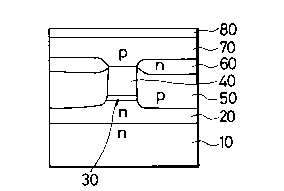
In Fig. 1, an n-type InP buffer layer 20, an
active layer region 30, a p-type InP clad layer 40, a
-- 8
2064681
-
p-type InP buried layer 50, an n-type InP buried layer
60, a p-type InP clad layer 70, and a p-type InGaAsP
contact layer 80 are respectively provided on an n-type
InP substrate lO.
The active layer region 30 is composed, as
apparent from the relationship between a layer
thickness and composition (wavelength ~ corresponding
to band gap) shown Fig. 2, of undoped first active
layer 31 and p-type second active layer 32 formed of
quantum well structure, a p-type InP intermediate clad
layer 33, a n-type GRIN-SCH structure layer 34 and an
p-type GRIN-SCH structure 35.
In the relative relation, the intermediate clad
layer 33 is interposed between the first active layer
31 and the second active layer 32 adjacently, one
GRIN-SCH structure 34 is provided under the first
active layer 31, and the other GRIN-SCH structure 35 is
provided on the second active layer 32.
The above-described layers are formed on the
n-type InP substrate 10, for example, mainly by a
vapor-phase epitaxial method. More specifically, a
vapor-phase epitaxial method such as an MOCVD method
having excellent controllability for the thickness,
composition of a thin film is employed, the layers are
formed as below.
206~681
An n-type InP buffer layer 20 having 1 x 1018cm~3
of carrier concentration and 2 ~m of thickness is first
grown on an n-type InP substrate 10.
Then, as an n-type GRIN-SCH structure 34 in which
its refractive index is reduced gradually from the
first active layer 31 to n-InP buffer, a thin film 34a
having ~ (band gap wavelength) = 0.95 ~m, a thin film
34b having ~ (band gap wavelength) = 1.05 ~m, a thin
film 34c having ~ (wavelength composition) = 1.0 ~m and
a thin film 34d having ~ (band gap wavelength) = 1.1 ~m
are sequentially formed on an n-type InP buffer layer
20 with carrier concentration = 1 x 1017cm~3, thickness
= 30 nm.
The n-type GRIN-SCH structure layer 34 is formed,
for example, of InGaAsP thin films 34a, 34b, 34c and
34d so as to exhibit a quasi-parabolic state.
In this case, when the InGaAsP compositions of the
thin films 34a, 34b, 34c and 34d are continuously
varied, more preferable n-type GRIN-SCH structure layer
34 is obtained.
Then, a p-type first active layer 31 having a
quantum well structure, formed of three wells 31a
having ~ (band gap wavelength) = 1.32 ~m and thickness
= 13 nm, and two barriers 3lb having ~ (band gap
wavelength) = 1.1 ~m and thickness = 15 nm is formed on
-- 10 --
206~681
the n-type GRIN-SCH structure layer 34 corresponding to
three periods.
Subsequently, a p-type GaInAsP intermediate clad
layer 33 having ~ (band gap wavelength) = 1.1 ~m,
carrier concentration = 5 x 1017cm~3, thickness = 50 nm
is laminated on the first active layer 31.
The intermediate clad layer 33 of this case is set
to a thickness of about 50 nm as exemplified above so
as to prevent duplication of wave functions of
electrons of the first and second active layers 31 and
32. Further, in order to sufficiently supply holes to
the first active layer 31, InP is Zn-doped as
exemplified above.
Then, a p-type second active layer 32 having a
quantum well structure, formed of three wells 32a
having ~ (band gap wavelength) = 1.32 ~m, thickness =
12 nm and two barriers 32b having ~ (band gap
wavelength) = 1.1 ~m, thickness = 15 nm is grown on the
p-type GaInAsP intermediate clad layer 33 similarly
corresponding to three periods.
The well width of the p-type second active layer
32 is shortened so that the second active layer has
larger confinement energy than that of the first active
layer 31.
Therefore, the second active layer 32 acts as an
-- 11 --
206~681
less absorption layer for the light of the first active
layer 31.
Subsequently, as an p-type GRIN-SCH structure
layer 35 having a refractive index reducing gradually
from the second active layer 32 to p-clad layer 40,
a thin film 35a having ~ (band gap wavelength) = 1.1
~m, a thin film 35b having ~ (band gap wavelength) =
1.0 ~m, a thin film 35c having ~ (band gap wavelength)
= 1.0 ~m and a thin film 35d having ~ (band gap
wavelength composition) = 0.95 ~m are sequentially
formed on the first active layer 31 with carrier
concentration = 1 x 1017cm~3, thickness = 30 nm.
Further, a p-type InP clad layer 40 is laminated
0.5 ~m thick on the p-type GRIN-SCH structure layer 35.
After the layers are formed on the n-type InP
substrate 10, SiO2 stripes having 2~m of width along a
direction "011" are formed on the epitaxial wafer as
etching masks, and layers including p-clad 40, active
30, and the portion of the n-type InP buffer layer 20
are wet etched except the mask portion. Thus, mesa
stripes are formed on the n-type InP substrate 10.
Then, a p-type InP buried layer 50 and an n-type
InP buried layer 60 are sequentially grown at both
sides of the mesa stripes.
Thereafter, the SiO2 mask is removed, and a p-type
- 12 -
206~6~1
InP clad layer 70 having carrier concentration = 8 x
1017cm~3, thickness = 2 ~m and a p-type InGaAsP
contact layer 80 having carrier concentration = 1 x
1018cm~3, thickness = 0.5 ~m are sequentially grown on
the upper surface of the epitaxial wafer.
Subsequently, the n-type InP substrate 10 is
lapped from the rear surface side, the substrate 10 is
finished to thickness of 100 - 150 ~m, n-type electrode
(not shown) is formed on the rear surface of the
substrate, and a p-type electrode (not shown) is formed
on the upper surface (contact layer 80 side) of the
epitaxial wafer.
The above-described first and second active layers
31 and 32 may have a single quantum well structure or a
multiple quantum well structure.
As other embodiment, only one of a first active
layer 31 and a second active layer 31 may have a
quantum well structure. In this case, a refractive
index distribution region (GRIN-SCH structure) is
provided at the one active layer side.
When a current is injected between the p-type
electrode and the n-type electrode in the semiconductor
laser diode shown in Fig. 1, the active layer region
30 radiates a light, the radiated light is reflected
and amplified in the active layer region 30 to cause a
206~681
laser operation therein, and the active layer region 30
inductively irradiates a light therefrom in a
predetermined direction.
Since the first and second active layers 31 and 32
are formed of the quantum well structure as described
above, the threshold current density is low, the laser
light absorption by the second active layer 32 is
small, thereby preventing the threshold current density
from increasing.
The validity of the GRIN-SCH structure layers 34,
35 are as will be described below.
A mode gain rgth is balanced with total loss at
the threshold of laser oscillation as by the following
equation (2), where r is light confinement factor of
the quantum well structure of the active layer, and g
is gain.
rgth = ~i + [(l/L) ln (l/R)] (2)
where ~i: loss of waveguide
(l/L) ln (l/R): term indicating reflection loss of
resonator mirror
L: length of resonator
R: reflectivity
The gain g is represented by the following
equation (3) in term of a junction current density J.
g = ~ [(~i/d) J - JO] (3)
- 14 -
2064681
where ~: gain constant
~i: internal quantum efficiency
d : thickness of the active layer
Jo: current density for forming g = O condition.
As evident from the equations (2) and (3), if J =
Jth is satisfied, g = gth is obtained. Therefore, the
Jth becomes as the following equation (4).
Jth = (JO d/~i) + (d/~i~r)~i +
(d/~i~r)[(l/L) ln (1/R)] (4)
In the equation (4) described above, the three
terms of the right side are respectively an intrinsic
term, an absorption term and a mirror loss term, and
the dependence on the active layer thickness of the
respective terms become as shown in Fig. 3 (refer to
reference 3 below).
I = Jo d/~i: intrinsic term
A = (d/~i~r)~: absorption term
M = td/~i~r~) [(1/L) ln (1/R)]: mirror loss term
Reference 3: Appl. Phys. Lett., Vol 40, No.3,
pp.217-219 (1982)
In the conventional DH structure indicated by a
solid line in Fig. 3, the r is proportional to the
square of the d. Accordingly, in case of d < 0.07 ~m,
the absorption term A and the reflection loss term M
become larger than the intrinsic term I, and the Jth is
- 15 -
206468~
abruptly raised.
On the contrary, in the GRIN-SCH structure shown
by a broken line in Fig. 3, the r itself is larger than
that of conventional one and (r/d) is constant,
therefore the absorption term A and the reflection loss
term M are constant and smaller than those of
conventional one. Accordingly, if the d is reduced,
the Jth is not raised, but reduced as the intrinsic
term I is proportional to d.
In addition, in the laser diode having the
quantum well structure, the gain constant ~ is
increased by quantum effect. Therefore, the absorption
term A and the mirror loss term M are further reduced.
As described above, the GRIN-SCH structure is
associated with the quantum well structure, thereby
providing the semiconductor laser diode having low
loss and low threshold current density and particularly
the GRIN-SCH-MQW laser diode of 1.3 ~m region using the
InGaAsP.
According to a reference 4 below, the loss ~ of
the waveguide with the GRIN-SCH-MQW laser diode is ~ =
5cm~l .
Reference 4: J.J.A.P. Vol 28, No. 4, pp 661-663
(1989)
The above values are 1/3 of those of the
206~1~81
conventional bulk DH laser diode.
The reflection loss M of the GRIN-SCH-MQW laser
diode can be further reduced by enhancing the
reflectivity of the cleaved surface thereof.
Therefore, the threshold current can be further reduced
in the laser diode.
Furthermore, the reference 4 also discloses that a
longitudinal single mode oscillation was observed in a
wide temperature range in the GRIN-SCH-MQW-BH laser
diode. In a reference 5 below with respect to a DCC
structure, it was reported that similar longitudinal
single mode oscillation is obtained in a BC type laser
diode in which first and second active layers have
different widths.
Reference 5: Appl. Phys. Lett., Vol. 42, No. 12,
15 (1982)
From these reports, it is expected that more
preferable longitudinal single mode oscillation can be
obtained in the MQW-DCC laser diode of the present
invention.
Fig. 4 shows an optical output-current
characteristic of a semiconductor laser diode
according to the present invention and a conventional
bulk DCC laser diode, and Fig. 5 shows temperature
dependency characteristic of threshold current and
- 17 -
2064681
external differential quantum efficiency (per one
facet) of the semiconductor laser diode according to
the present invention.
In the case of Fig. 5, the variation of the
threshold current is expressed by a ratio to a
threshold current Itho at 20C.
The semiconductor laser diode according to the
present invention provides of about 15 mA of the
threshold current which is about a half of that of
a conventional bulk DCC laser diode.
Further, in the case of the semiconductor laser
diode according to the present invention, as apparent
from Fig. 5, its characteristic temperature To is 180
K. This value is equivalent to that of the bulk DCC
and more preferable than that of the conventional bulk
DH.
In addition, the semiconductor laser diode
according to the present invention provides a small
decrease in the light confinement rate at a high
temperature similarly to the bulk DCC and raises the
light confinement rate by incorporating the quantum
well structure and the GRIN-SCH structure together.
As another embodiment of the present invention, a
semiconductor laser diode in which an SCH structure is
a step type SCH structure will be described with
- 18 -
2064681
reference to Fig. 6.
In the case of the semiconductor laser diode
exemplified in Fig. 6, the feature that step type SCH
structure layers 34 and 35 are formed of thin films
34a, 34b and thin films 35a, 35b, is different from
that as described with reference to Fig. 2, but the
other technical content is the same as those as
described with reference to Figs. 1 and 2.
A semiconductor laser diode exemplified in Fig. 6
can also prevent an increase in a threshold value
current density depending upon the step type SCH
structure layers 34 and 35.
The semiconductor laser diode according to the
present invention provides a semiconductor laser diode
of pn double hetero junction type which comprises a
first active layer formed on a substrate, a second
active layer adjacent to the first active layer in such
a manner that at least one of said first and second
active layers is formed of multi quantum well or single
quantum well structure, an intermediate clad layer
interposed between said first active layer and said
second active layer, and an SCH structure provided on
at least one of under said first active layer and over
second active layer. Therefore, the semiconductor
laser diode of the invention can reduce the threshold
2064681
current at the time of laser oscillation, and obtain
preferable operation characteristics even under severe
environment of temperature condition.
- 20 -