Note : Les descriptions sont présentées dans la langue officielle dans laquelle elles ont été soumises.
- 1 - FJ-~656/PC'r
DESCRIPTION
Asynchronous Signal Extracting Circuit
TECHNICAL FIELD ?
The present invention relates to an asynchronous
signal extracting circuit for extracting asynchronous
signals that are multiplexed in a synchronization frame.
BACKGROUND ART
A synchronous digital hierarchy (SDH) for
transmitting asynchronous signals in a multiplexed form
in a synchronization frame has been standardized as
recommended by CCITT ~International Telegraph and
Telephone Consultative Committee~ and Tl Committee of
U.S~A. In the synchronous digltal hierarchy, it is
necessary to extxact asynchronous signals from the
received signals in order to obtain valid data
accompanying almost no jitter~ '
In the synchronous digital hierarchy (SDH)
rec~- - ded by CCITT, a difference in speed between the
.
synchronous system and the asynchronous system is
corrected by a pointer adjustment function; i.e., valid ~:
data consisting of eight bits is inserted or deleted by
the pointer adjustment, and a phase jump of eight bits ;~ -
takes place in the formation payload~ The phase jump
causes jitter that is given to asynchronous signals ~ :
:
.. , .. , .. ..... , . ~ : :
.i 3
extracted ~rom the synchronous multiplexed signals that
are receiveA. On the receiving side, therefore, the
jitter must be suppressed by using phase-locked loop
circuit or a like circuit.
On the receiving side in the conventional
synchronous digital hierarchy as will be described later
in detail, valid data only are written using a buffer
memory when the asynchronous signals are to be extracted
by receiving synchronous multiplex signals, and the valid
data are read out according to read clock signals. Here,
the write clock signals of a buffer memory have an
untoothed period that varies depending upon the presence
or absence of pointer adjustment, and the moment at which
the pointer adjustment takes place is not definite,
resulting in the occurrence of low-frequency jitter as
described above.
As a means for xeducing the low-frequency jitter,
for example, the Contribution (TlX1.6/89-020R2) of TlXl.6
of U.S.A. discloses circuit constitutions and problems.
The circuit constitutions are:
(1) A desynchronizer (asynchronous signal
extractlng circuit) equipped with a PLL of a very low
frequency band;
(2) A synchronous desynchronizer;
(3) A fixed bit leak constitution (using PLLs in
two stages); ~nd
~,~ . : ,
- 3 -
(4) A two-stage PLL of the linear digital control
type.
The constitution (1) requires a PLL of a frequency
band as narrow as about 3 Hz with which it is dif~icult
to r~alize a practical circuit.
The constitution (2) requires digital control that
adapts to the monitoring of a buffer memoxy, which
results in a complex circuit constitution and control
operation.
In the constitution (3), the bits slowly leak over a
given period of time as the pointer adjustment takes
place, and the jitter component decreases. Here,
however, the buffer memory must have an extra capacity to
cope with the pointer adjustment that takes place
continuously.
The constitution (4) requires a digital filter or a
dither~ causing the circuit constitution to become
comple~.
DISCLOSURE OF THE lNv~NllON
In view of the above-men~ioned defects, the object
of the present invention is to suppress the low-frequency
jitter relying upon a simple constitution.
In order to achieve the above object according to
the present invention, a control is applied to the
frequency band of a low-pass filter mounted in a phase-
locked loop circuit that forms the read clock signals
: . -:, .: ,.. ... . . . . . .. . ...... - . . ,
.,: .. . ,. .,. , , .. :.. ,.,., ,. : - , . - . : . :
- 4 _
that will be applied to the buffer memory. The low-
frequency ~itter i5 suppressed by controlling the
frequency band.
BRIEF DESCRIPTION OF DRAI~INGS
The invention will now be described with reference
to the accompanying drawings ~erein:
Fig. 1 is a block diagram showing major portions of
the receiving side in a conventional synchronous digital
hierarchy;
Figs. 2A to 2H are diagrams of signals for
explaining the operation of the conventional example of
Fig. 1;
Fig. 3 is a block diagram showing the principle and
constitution of an asynchronous signal extracting circuit
according to the present invention;
Fig. 4 is a block diagram showing the asynchronous
signal extracting circuit according to an embodiment of
the present invention;
Figs. 5A to 5D are diagrams of signals for
explaining the wri~e clock signals and the read clock
signals;
Fig. 6 is a diagram for explaining the operation
based upon a first concrete example of the present
invention;
Figs. 7A to 7C are diagrams for explaining the
operation based upon a second concrete example of the
- ~ . -: . -: . ,;
.-: : : - , - .
;'53
-- 5
present invention;
Fig. 8 is a diagram for explaining the operation
based upon a third concrete example of the present
invention;
Fig. 9 is a diagram for explaining the operation
based upon a fourth concrete example of the present
invention;
Fig. 10 is a diagram for explaining the operation
based upon a fifth concrete example of the present
invention; ;~'
Fig. 11 is a diagram for explaining the operation
based upon a sixth concrete example of the pres~nt
invention;
Fig. 12 is a diagram for explain;ng the operation
based upon a seventh concrete example of the pxesent
invention;
Fig. 13 is a diagram for explaining the operation ' -
based upon an eighth concrete example of the present
invention;
Fig. 14 is a diagram for explaining the operation
based upon a ninth concrete example of the present
invention;
Fig. 15 is a diagram for explaining the operation
based upon a tenth concrete example of the present
invention; ~ .
Fig. 16 is a block diagram illustrating the
. :. : .
- 6 - 2~~~ ~ ~ L~J~,~
constitution based upon an eleventh concrete example
embodiment of the present invention;
Fig. 17 is a block diagram illustrating the
constitution based upon a twelfth concrete example
embodiment of the present invention;
Fig. 18 is a diagram illustrating the control unit
of Fig. 4 in detail;
Figs. l9A to l9D are diagrams of signal waveforms
appearing at major portions of the circuit of Fig. 18;
Fig. 20 is a diagram showing in detail the low-pass
filter (Fig. 4) that is controlled by the control ~mit of
Fig. 18; and
Fig. 21 is a diagram showing in detail the control
unit of Fig. 16.
BEST MODE FOR CARRYING OUT THE lNV~N'l'lON
Prior to describing the present invention, the
constitution of the receiving side in the aforementioned
conventional synchronous digital hierarchy will be
described with reference to the drawings.
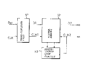
Fig. l is a block diagram of major portions of the
receiving side in the conventional synchronous digital ;~
hierarchy, and Figs. 2A to 2H are diagrams of signals for
explaining the operation of the conventional system.
Synchronous multiplexed signals Din and input clock
signals C~ in synchronism therewith are applied to a
demultiplexer llnit 51 ~rom a receiving unit that is not
- ~ .:
.. . . .
5.~
-- 7 ~
shown. The demultiplexer unit 51 detects the presence of
poin~er adjustment and gives write clock signals CBK 1
that indicate valid data to a buffer memory 52. The
write clock signals CLK 1 for:m a pulse train that is
untoothed in the portions of invalid data. The input
data Dl are written into the :buffer memory 52 in
accordance with the write clock signals CLK 1.
The data D2 are read out from the buffer memory 52
by continuous read clock signals C~K 2 which are brought
into synch.ronism in phase with the write clock signals
CLK 1 by a phase-locked loop circuit (hereinafter
referred to as PLL) 53 which, in general, is comprised of
a phase comparator that compares the phase of write clock
signals CLK 1 with the phase of read clock signals CLK 2,
a low-pass filter which lell,oves high-frequency components
from a resultant phase comparison output signal, and a
voltage controlled oscillator which oscillates being
controlled by the output signal of the low-pass filter :
and outputs the read clock signal directly or by dividing
its frequency. :
When the input data D1 and the write clock signals :
C~K 1 are as shown in Figs. 2A and 2B where there is no
pointer adjustment and when the invalid data are deleted
by the pointer adjustmen-t, i.e., a minus pointer :~
adjustment takes place, they become ~s shown in Figs. 2C
and 2D. In the case when the invalid data are inserted
~ , ~: : . : , . .
,. . : ~:
.
5~3
by the pointer adjustment, i.e., in the case of a plus
pointer adjustment, the data become as shown in Figs. 2E
and 2F and the phase jump of eight bits takes place as
described above.
As shown in Figs. 2G and 2H in an exaggerated
manner, the read data D~ and the read clock signals C~K 2
from the buffer memory 52 have different periods in the
rising timing due to the phase jump. Therefore, the
pointer adjustment is in many cases carried out
maintaining a relatively long random period, and hence
low-frequency jitter is contained in the read clock
signals CLK 2.
The above-mentioned four circuit constitutions (1),
(2), (3) and (4) have been known as a means for
decreasing the low-frequency jitter involving, however,
their inherent defects as mentioned above. The
asynchronous signal extracting circuit of the present
invention, which is free from the above-mentioned ~ -
defects, will now be described in detail.
Fig. 3 is a block diagram illustrating the prînciple
and constitution of the asynchronous signal extracting
circuit according to the present invention.
The circuit comprises:
a demultiplexer unit 1 which demultiplexes
asynchronous signals multiplexed in a synchronization
frame and clock signals in synchronism with ~alid data in
.. .. :
~ . . . - , . . "- , .
_ 9
the asynchr~nous signals;
a buffe.r memory 2 th.at writes valid data in the
asynchronous signals demultiplexed by the demultiplexer
unit 1 using the clock signals from the demultiplexer
unit 1 as write clock signals;
a pnase-locked loop circuit 3 that forms read
clock signals for the buffer memory 2; and
a control unit 5 that switches the frequency
band of a low-pass filter 4 in the phase-locked loop
circuit 3 periodically or in response to a detection
signal of pointer adjustment in the demultiplexer unit 1.
Here, the phase-locked loop circuit 3 is constituted by a
phase comparator 6 that compares the phase of write clock
signal with the phase of read clock signal, the aforesaid
low-pass filter 4, a voltage controlled oscillator 7, and
a frequency divider 8.
The control unit 5 may be constituted so as to
continuously, or in steps, switch the frequency band of
the low-pass filter 4 in a predetermined period.
The control unit 5 fur her may be constituted so as .
to successively narrow the frequency band of the low-pass
filter 4 every time a detection signal of pointer
adjustment in the asynchronous signals is obtained in the
demultiplexer unit 1 within a predetermined period of
time and return the frequency band of the low-pass
filter 4 to the initial frequency band gradually or at a
~ : :
.. ,.. , . .. , ~
. :. : : . .. , . - . - . . . .
-
~ 10 -
time when the detection signal of invalid data i~ not
obtained within a predetermined period of time.
The embodiment of the present invention can be
modified in a variety of ways~ The phase-locked loop
circuit 3 may be constituted by a counter that ~ounts the
phase difference between the write clock signal of buffex
memory 2 and read clock signal, and a frequency divider
of which the frequency-dividing ratio is controlled when
the counted content of the counter has reached a setpoint
value and produces a frequency-divided output signal as a
read clock signal.
The control unit 5 may be constituted so as to
switch the frequency band of the low-pass filter by
changing the setpoint value of counted content of the
counter.
It is further possible to constitute the buffer
memory 2 and the phase-locked loop circuit 3 in two
stages, wherein the read clock signal from the phase-
locked loop circuit of the first stage to the buffer
memory of the first stage is used as a write clock signal
for the buffer memory of the second stage, and the read
clock signal for the buffer memory of the second stage is
formed by the phase-locked loop circuit of the second
stage, and wherein a control unit can be provided to
control the frequency band of the low-pass filter in the
phase-locked loop circuit of either the first stage or
: . . .:~ : :.
. : .: ; : , . :. ., , . . .::
.. . . . : ~, ,
.. ... . .
the second stage.
It is possible to provide a control unit that
controls the frequency bands of low-pass filters in the
phase-locked loop circuits of the first stage and the
second stage in a complementary manner, i.e., in a manner
that the frequency band of the low-pass filter of one
phase-locked loop circuit is narrowed when the frequency
band of-the low-pass filter of the other phase-locked
loop circuit is broadened.
Next, the operation of the above-mentioned principle
and constitution will be described.
Valid data only are written into the buffer memory 2
by the write clock signals at which the invalid data -
portions are untoothed, and are read out by the read
clQck signals. The read data and read clock signals are
transferred to a processing circuit or the like circui~
in the next sta~e, which is not illustrated.
The low-frequency jitter can be suppressed by ~ ;
narrowing the frequency band of the low-pass filter 4 in
the phase-locked loop circuit 3 resulting, however, in an -
..
increase in the time required for pulling in the phase
synchronization. Therefore, the frequency band of the
low-pass filter 4 is perlodically switched to a usual
frequency band (e.g., 100 Hz) and a narrow frequency band
(e.g., 3 Hz) in response to a switch control signal from
the control unlt S in order to equivalently narrow the
- 12 _ ~ ?~
frequency band of the low-pass filter 4 and suppress the
low-frequency jitter without. lengthening the time for
pulling in the phase synchronization.
It is further possible to narrow the frequency band
of the low-pass filter 4 at a moment when the pointer
adjustment takes place thereby to suppress the low-
frequency jitter due to the pointer adjustment without
lengthening the time for pulling in the phase
synchronization.
It i5 further possible to switch the frequency band
of the low-pass filter 4 not only to broad band and
narrow band but also to a plurality of frequency bands
continuously, or in steps, in order to gradually change
the phase in the read clock signals and stabilize the
~...
operation of the phase-locked loop circuit 3.
When the detection signals of pointer adjustment are
repetitively obtained within a predetermined period of
time, i.e., it means that the low-frequency jitter is
contained in large amounts. Therefore, the frequency
band of the low-pass filter 4 is controlled each tima to
gradually become narrow. This makes it possible to
suppress the low-frequency jitter from increasing. Here,
the minimum frequency band may have been determined in
advance so that the frequency band will not become
narrower than this band. When the detection signal of
pointer adjustment is not obtained within predetermined
:
;~r~ 3
- 13 -
period of time, the frequenc~ band of the low-pass
filter 4 is returned to the usual ~requency band
gradually or at on~ time.
Moreover, the phase-locked loop circuit 3 may be
constituted in a digitally controlled type wherein a
phase difference between the write clock signal and the
read clock signal of the buffer memory 2 is counted up or
is counted down by a counter; the frequency-dividing
ratio of the frequency divider is controlled to become ~
great or small when the counted content of the counter -
has reached a count-up setpoint value or a count-down ~;
~ ~:
setpoint value; the frequency-divided output sign~l of
the frequency divider is used as a read clock signal for -
the buffer memory 2, and the setpoint value of counted ~ .
content of the counter is changed by the control unit so
that the counter acts like the low-pass filter.
~ ~
Therefore, the frequency band of the low-pass filter can
be switched in a digital manner. The frequency band can
be switched periodically or depending upon a detection
signal of pointer adjustment. -;
When the buffer memory 2 and the phase-locked loop
circuit 3 are each constituted in two stages and when the
fre~uency band of the low~pass filter in either one of ;-
the phase~locked Ioop circuits at least is periodically
switched by the control unit, the modulation frequency
may appear as a jitter component that can be easily
Z~ 5~3
- 14 -
removed by selecting a modulation frequency component
outsid~ the frequency band of the phase-locked loop
circuit of the second stage.
It is further possible to suppress low-frequency
jitter without increasing the time for pulling in the
phase synchronization by contl~olling the frequency bands
of low~pass filters in the phase-locked loop circuits of
the first and second stages in a complementary manner,
i.e., one frequency ~and is narrowed when the other one
is broadened.
~ mbodiments of the present invention will now be
described in detail with reference to the accompanying
drawings.
Fig. 4 is a block diagram illustrating the
asynchronous signal extracting circuit according to an
embodiment of the present invention, wherein reference
numexal 11 denotes a demultipl~xer unit, 12 denotes a
buffer memory, 13 denotes a phase-locked loop circuit, 14
denotes a low-pass filter~ 15 denotes a control unit, 16
denotes a phase comparator, 17 denotes a voltage
controlled oscillator, 18 denotes a frequency divider, 19
denotes a processing unit, 20 denotes an output unit, 21 ;~
and 22 denote ring counters, and reference numeral 23 ;
denotes a memory.
Synchronous multiplexed signals Din and input clock
signals CLK are applied to the demultiplexer unit ll
.... . :
: . .
- 15 -
which are given ~rom a receiving unit, not shown; input
data Dl of asynchronous signals demultiplexed from the
synchronous multiplexed signal~s Din and write clock
signals CLK 1 representing valid data are applied to the
buffer memory 12, and a detection signal "a" of invalid
data by the pointer adjustment and a synchronization
frame detection signal "b" are applied to the control
unit 15.
Figs. 5A and 5D are signal diagrams explaining the
write clock signals and the read clock signals. The
valid data and write clock signals CLK 1 of the above
case become, as shown in, for example, Figs. SA and SB.
That is, the write clock signals CLK 1 form an untoothed
pulse train corresponding to invalid data. .
The bu~fer memory 12 in this embodiment is
constituted by a ring counter 21 that operates iTl
response to the write clock signals CLK 1, a ring
counter 22 that operates in response to the read clock
signals CLK 2, and a memory 23 that writes the input
data Dl onto an address specified by the ring counter 21
and reads the data D2 from an address specified by the
ring counter 22. The buffer memory 12, however, may be -
constituted in other ways.
The write clock signals CLX 1 and the read clock
signals CLK 2 applied to the buffer memory 12 are further
applied to the phase comparator 16 in the phase-locked
,. . . . ,,. : , , , , . , ,.: .
,
,~: ',, :.,,, :
',
~?~
-- 16 --
loop circuit 13 and are compared with regard to their
phases. The phase comparison output signal passes
through th~ low-pass filter 14 and serves as a control
voltage for the voltage controlled oscillator 17, which
controls the oscillation frequency. Output signals of
the voltage controlled oscillator 17 are divided by the
frequency divider to form reacL clock signals CLK ~. The
read clock signals CLK 2 become, as shown in, for
example~ Fig. 5D and the read data D2 become as shown in,
for example, Fig. 5C, and whereby the valid data written
into the buffer memory 12 are read out and are
transferred to a processing circuit in the next stage
together with the read clock signals C~K 2.
The control unit 15 is constituted by the processing
unit 19 and the output unit 20 that applies switch
control signal "d" to the low-pass filter 14. Detectlon :
signals "a and b" from the demultiplexer unit 11, and a
line condition change signal "c" from a line changing
unit not shown, are applied to the processing unit 19 ~ -~
that is constituted by a microprocessor or the like and :
executes the processing continuously or in steps to
switch the frequency band of the low-pass filter 14 in
the phase-locked loop circuit 13 either periodically or
in response to the detection signals ~'a and b" or the
line condition change signal l'c~
Fig. 6 is a diagram explaining the operation based
.
' :'
~ ~ . - , . . : :
,~?~ 3
on the first concrete example of the present invention
wherein th~ frequency band of the low-pass filter 14 is
switched to two steps of fl and f2 at a predetermined
period T determined by a timer or the like of the
processing unit 19. That is, Fig. 6 shows the case where
the usual frequency band f2 is, for exampl~, 100 Hz, a
narrow fre~uency band fl is, ~or example 3 Hz, and
tl + t2 = T where tl is the time o~ the frequency band fl
and t2 is the time of the frequency band f2. Therefore,
the low-pass filter 14 equivalently acts as a frequency
band narrower than the usual frequency band f2 and
suppresses the low-frequency jitter without sacrificing
the time for pulling in the phase synchronization.
Fig. 7~ to 7C are diagrams for explaining the
operation based on a second concrete-example of the
presênt invention where the frequency ~and of the low-
~requency filter 14 in the phase-locked loop circuit 13
is switched continuously or in steps and wherein Fig. 7A
illustrates the case where the frequency band of the low-
frequency filter 14 is broadened in steps as indicated by .
fl, f2, ---, fn, and returned to the narrowest frequency
band fl after the frequency band fn main~;n;ng a period
T. Fig. 7B illustrates the case where the frequency band
of the low-pass filter 14 is broadened in steps as '
indicated by fl, f2, ---, fn and is then narrowed in
steps toward the narrowest frequency band fl after the ~ ~
'~ ' .
?~3
- 18 -
frequency band fn maintain a period T. Fig. 7C
illustrates the case where the frequency band of the low-
pass filter 14 is controlled like a folded line as
indicated by fl, f2, ---, fn, and is returned to the
narrowest frequency band fl after the frequency baTld fn
maintain a period T. Here, the frequency band that is
controlled like a folded line may further be linearly or
curvedly controlled.
There may be provided a func-tion for generating a
frequency band switching control curve of any one of the
above-mentioned Figs. 7A to 7C or other frequency band
switching control curves. The function may be exhibited
by the processing unit 19 or a function generating
circuit may be added to realize the above frequency band
switching control.
Fig. 8 is a diagram for expl~i ning the operation
based on a third concrete example of the present
invention in the case when the frequency band of the low-
pass filter 14 in the pha~e-locked loop circuit 13 is
switched in synchronism with a synchronlzation frame '~
signal of synchronous multiplexed signals. A detection
signal ~b" of a synchronization frame signal is applied
to the control unit 15 from the demultiplexer unit 11.
Like in first concrete example (Fig. 6), therefore, the
processing unit 19 executes the operatîon based on the
detection signal ~b~ in a manner of tl : t2 = 3 : 2 where
. .
~ ~ , , : ::: :,
, . ..
~ 3
- 19 -
the period T is the sum of the time t2 of the frequency
band f2 and th~ time tl of the frequency band fl. Here,
the ratio of time tl to time t2 may be varied. It is
furthex possible to continuously or in steps control the
frequency band of the low-pass filter 14 as in the second
concrete example (Figs. 7A to 7C).
Fig. 9 is a diagram exp~i n; ng the operation based
on a fourth concrete example of the present invention
where tne frequency band of the low-pass filter 14 in the
phase-locked loop circuit 13 is switched upon detecting
the point adjustment PA in the demultiplexer unit 11.
The low-pass filter 14 has a usual frequency band f2.
When the pointer adjustment PA is detected at the ~-
demultiplexer unit 11 and the detection si~nal "a"
thereof is applied to the control unit 15, the processing
unit 19 in the control unit 15 works so as to give a
switch control signal "d" from the output unit 20 to the
low-pass filter 14 to switch the low-pass filter 14 into
a narrow ~requency band fl for a predetermined period of
time TS only. Then, the low-pass filter 14 is switched
to the narrow frequency band fl for the period of time TS
only. After the lapse of time TS, the frequency band is
returned to the initial frequency band f2 at one time, or ;~
is returned in steps to the initial frequency band f2 as
indicated by a dotted line, or is continuously returned
to the initial frequency band f2.
'
- 20 -
Thus, the fxequency band of the low-pass Eilter 14
is narrowed upon detec~.ing the pointer adjustment P~
making it possible ~o suppress the insertion of invalid
data caused by pointer adjustment PA or suppress the low-
frequency jitter caused by deletion.
Fig. 10 is a diagram exp:Laining the operation based
upon a fifth concrete example of the present invention in
the case when the pointer adjustment PA has repetitively
taken place. The frequency band of the low-pass
filter 14 is switched from the usual frequency band f2 to
the narrow frequency band fl upon the detection of
pointer adjustment PAl, and is switched again before the
predeterm;ned period of time TS lapses to the narrow
freguency band fl for the predetermined period of time TS
from the moment of detection when the next pointer
adjustment PA2 is detected, i.e., when TS > t3. After
the lapse of time TS, the frequency band is returned to
the inîtial frequency band f2.
When the next pointer adjustment PA3 is detected
after the frequency band is returned to the initial
frequency band f2, the control operation is carried out
again to switch the frequency band to the frequency
band fl for the period of time TS only. That is, the
control operation is carried out to switch the frequency
band of the low-pass filter 14 from f2 into fl based on
the similar action to that of a retriggerable monostable
.,
~ '~?"r~ .''3~3
- 21 -
multivibrator, which is triggered by the detection
signal ~a~ of the pointer adjustment PA.
Fig. 11 is a diagram exp].aining the operation based
on a sixth concrete example of the present invention in
the case when plus (+) and minus ( ) pointer
adjustments PA have taken plac:e. When, for example, the
pointer adjustment PA of the first time is a plus (~)
one, the frequency band of the low-pass filter 14 is
switched from the usual frequency band f2 to the narrow
frequency band fl upon the detection thereof and when the
pointer adjustmenk PA of the second time within the
predetermined period of time TS is a minus (~) one, the
direction of the lncreasing or decreasing low-frequency
jitter becomes opposite and the frequency band of the
low-pass filter 14 is returned to the usual frequency '
band f2. When the minus (-) pointer adjustment PA is
detected during the period when the frequency band of the ~-
low-frequency filter 14 is the:usual frequency band f2, :.
the control operation is carried out to switch the
frequency band to the narrow frequency band fl.
Fig. 12 is a diagram for explaining the operation :~
based on a seventh concrete example of the present :.
invention, which is a modification from the fifth
concrete example (Fig. 10), and wherein when the usual
frequency band f2 is switched to the narrow frequency
band fl, a ~ r value of tlme of the frequency band fl
i .. ..... .... .. .
- . : , :. - . : . . ~ . : .
~ ~S?5
- 22 -
is defined as TZ (> TS) and the frequency is forcibly
returned to the usual frequency band f2 when a period of
time long0r than the above has passed. For instance, the
usual frequency band f2 is switched to the narrow
frequency band fl upon detection of pointer adjustmenk PA
of the first time, the condition of the narrow frequency
band fl continues upon the detection of pointer
adjustment PA of the second time after a period of
time t5 that is shorter than the predetermined period of
time TS and, then, the condition of narrow frequency
band fl continues upon the detection of pointer
adjustment PA of the third time after a period of time t6
that is shorter than the predetermined period of time TS.
When the maximum setpoint time TZ lapses from when the
pointer adjustment PA of the first time îs detected, the
frequency band is forcibly returned to the initial
frequency band f2. This makes it possible to suppress
the low-frequency jitter, to limit the time for staying
in the narrow frequency band ~1, and stabili~e the
operation of the phase-locked loop circuit 13.
Fig. 13 is a diagram for expl~in;ng the operation
based on an eighth concrete example of the present ~.
invention in the case where the frequency band of the ~:
low-pass filter 14 is to be switched to fl, f2 and f3,
upon every detection of the pointer adjustment PA. That
is, the frequency band of the low-pass filter 14 that is
: -
.
- 23 -
the usual frequency band f3 is switched to a narrow
frequency band f2 upon the detection of pointer
adjustment PA of the first time, and is further switched
to a narrower frequency band fl upon the detection of
pointer adjustment PA of the second time within the
predetermined period of time TS. The frequency band has
already been switched to the mini~l~m frequency band fl
when the pointer adjustment PA of the third time is
detected within the predetermined period of time TS, and
this condition is maintained. Then, when the next
pointer adjustment PA is not detected within the
predetermined period of time, the control operation is
carried out to return the frequency band to the initial ~:
frequency band f3. .
When the pointer adjustment PA of the fourth time is
detected under this condition, the frequency band f3 is
switched to the frequency band f2, which is then returned
back to the initial frequency band f3 when a next pointer
adjustment PA is not detected within the predetermined
period of time TS. In this example, the frequency band .
is returned to the initial frequency band f3 at one time~
It is, however, also possible to return, in steps, the ~ :
frequency band to the initial frequency band f3. After
the r~;rllm preset time TS has lapsed, furthermore, it is
possible to forcibly return the frequency band to the
initial frequency band f3 like in the seventh concrete
..
, .,
: . .
:: , '' - ' ~ ~ :, : .
- 24 -
example (Fig. 12). It is fur~her possible to carry out
the switching control operation using frequency bands in
numbers greater than fl, f2 and f3.
Fig. 14 is a diagram exp]aining the opera~ion based
on a ninth concrete example of the present invention
wherein in the usual operation mode, the frequency band
of the low-pass filter 14 is switched maintaining a
period T according to the first concrete-example shown in
Fig. 6, and the usual frequency band f2 is switched to
the narrow frequency band fl for the predetermined period
of time TS only upon the detection of the pointer
adjustment and is returned to the usual operation mode
after the lapse of the time TS. In the usual operation
mode, the frequency band is switched according to the
second and third concrete examples (Figs. 7i to 7C
and 8), and the frequency band is switched upon the
detection of pointer adjustment according to the fourth
to eighth concrete examples (Figs. 9 to 13) in ~ '
combination with the above examples.
Fig. 15 is a diagram explaining the operation based
on a tenth concrete example of the present invention
wherein in the usual operation mode, the frequency band
of the low-pass filter 14 is switched maint~;n;ng the
period T as in the a~orementionad examples and when a
line condition detection signal "c" produced by the
switching of lines is applied to the control unit 15 at a
.; : - ,. . . , ;, . ' ~:~ '
- 25 ~ lr3~
moment indicated by L, the processing unit 19 in the
control unit 15 forcibly returns the frequency band to
the usual frequency band f2 and returns it to the usual
operation mode again af-ter the lapse of a time ~L, which
is longer than the time necessary for pulling in the
phase synchronization. Therefore, even when the phase is
not synchronized because of the switching of the lines,
since the frequency band of the low-pass filter 14 in the
phase-locked loop circuit 13 is switched to the broad
frequency band f2, the phase synchronization can be
pulled in within a relatively short period of time.
Fig. 16 is a block diagram illustrating the
constitution based on an eleventh concrete example of the
present invention, wherein reference numeral 31 denotes a
demultiplexer unit, 32 denotes a buffer memory, 33
denotes a phase-locked loop circuit, 34 denotes a counter
that acts as a low-pass filter, 35 denotes a control ~
unit, 36 denotes a phase comparator, and 37 denotes a -
frequency divider. This example deals with the case
where a phase-locked loop circuit 33 of the digital
controlled type is used, and wherein synchronous
multiplexed signals Din are applied to the demultiplexer
unit 31, asynchronous signals Dl are demultiplexed, write
clock signals CLK 1 representing valid data are applied
to the buffer memory 32, and valid data only are written
into the buffer memory 32. The read data D2 by the read
~ .
:: -~ .: .
:
- 26
clock signals CLK 2 are transferred to the processing
circuit in the next stage together with the read clock ~;
signals CLK 2.
The phase~locked loop circuit 33 is constituted by
the phase comparator 36, the counter 34 and the frequency
divider 37. The phase comparator 36 compares the phase
of write clock signal CLK 1 with the phase of read clock
signal CLK 2; the resultant comparison output signal
serves as a control signal for a count up or count down
of the counter 34, the upper limit v~lue and the lower
limit value of the counted content of the counter 34 is
set by a control signal "d" from the control unit 35.
When, for example, the upper limit value is attained, a
control signal "e" is output to increase the~
frequency dividing ratio of ~he frequency divider 37 by
+1 and when the lower limit value is attainéd, a control
signal ~If~ is output to decrease the frequency-dividing
ratio of the frequency divider 37 by -1.
The frequency divider 37 divides the frequency of
external high-speed clock signals "g" to form read clock
signals CLK 2, and of which the frequency-dividing ratio
is controlled depending upon a phase difference relative
to the write clock signals CLK 1 to maintain synchronism
in phase with the write clock signals CLK 1~ Therefore, :
the setpoint value of the counter 34 for controllins the
frequency-dividing ratio is controlled by the control ~
.;
~: ' ' . ' '. . ' ' ' ' , , . ':'
- 27 ~ 3
unit 35 in order to switch the frequency band of the
low-pass filter. In this case, the setpoint value can be
switched continuously or in steps maint~in;ng the
period T, or the frequency band is switched to a narrow
frequency band for the predetermined period of time TS
only upon the detection of pointer adjustment.
For example, the TU-11 synchronous multiplexed
signals recommended by CCITT contain a V3 byte that can
be used for adjusting a difference in the clock
frequency. When the DS1 signal is to be extracted from
the TU-11 synchronous multiplexed signals, therefore,
synchronous signals Din of 1.728 Mb/s are input to the
demultiplexer unit 31. High-speed clock signals ~g" of
49.408 Mb/s are input to the frequency divider 37 to
divide the frequency by 32, and the read clock signals
CLK 2 become 1.544 Mb/s. The frequency-dividing ratio of
the fre~uency divider 37 is controlled so that the phase
of read clock signals CLK 2 are in synchronism with the ~ -
phase of write clock signals CLK 1 in which the invalid
data portions are untoothed, and the setpoint value of
the counted content of the counter 34 is controlled by
the control unit 35 to switch the frequency band of the
low-pass filter and suppress the low-frequency jitter as
in the aforementioned examples.
Fig. 17 is a block diagram illustrating the
cons~titution based on a twelfth concrete example of the
.. .
- 28 -
present invention, wherein reference numeral. 41 denotes a
demultiplexer unit, 42 and 46 denote buffex memories, 43
and 47 denote phase-locked loop circuits, 44 and 48
denote low-pass filters, 45 denotes a control unit, and
wherein the buffer memories 42, 46 and the phase-locked
loop circuits 43, 47 are constituted in two stages.
The read clock signal CLK 2 of which the phase is
brought by the phase-locked loop circuit-43 of the first
stage into synchronism with the write clock signal CLK 1
of the buffer memory 42 serves as a write clock signal to
the buffer memory 46 of the second stage, and the read
data D2 of the buffer memory 42 are written into the
buffer memory 46. Further, the write clock signal and
the read clock signal CLK 3, whose phase is synchronized
by the phase-locked loop circuit 47 of the second stage,
are applied to the buffer memory 46, and the read data D3
and the read clock signal CLK 3 are transferred to the
processing circuit of the next stage.
The low-pass filters 44 and 48 in the phase-locked
loop circuits 43 and 47 are controlled for their
frequency bands by the control unit 45, which is provided
in common for each of the stages. The control unit 45,
however, may be provided for each of the stages and it is
further possible to fix the frequency band of the
low-pass filter of either the first stage or the second
stage. For instance, when the frequency band of the
. .. : , . . . .
~: .~: . - ~ . . -
,.
.
~'' .. ' ' ' .
~ : :::, , .
~ .
- 29 -
low-pass filter 44 of the phase-locked loop circuit 43 of
the first stage is to be switched to fl, f2 maintaining
the period T, the frequency band of the low-pass
filter 48 of phase-locked loop circuit 47 of the second
stage is fixed, and the frequency band is selected so
that the modulation frequency component in the
phase-locked loop with the period T can be cut off by the
low-pass filter 48 of the second stage. ~Then, the jitter
is stably suppressed.
The freguency band of low-pass filters 44 and 48 of
the first stage and second stage can be switched in a
complementar manner. That is, when the frequency band of
the low-pass filter 44 of the first stage is fl, the
frequency band of the low-pass filter of the second stage
is set to be f2 and when the frequency band of the
low-pass filter 44 of the first stage is f2, the
frequency band of the low-pass filter 48 of the second
stage is set to fl. Similarly, even when the frequency
band of the low-pass filter is controlled upon detection ~;
of the point adjustment, the first stage and the second
stage can be switched in a complementar manner.
The present invention is not limited to the
aforementioned examples but encompasses the constitution
of a combination of these examples.
- Finally~ the control unit 15 shown in Fig. 4 and the
control unit 35 shown in Fig. 16 will be described in
. ~ I . - . .
~::
- : ,
'
- 30 -
detail.
Fig. 18 is a diagram illustrating in detail the
control unit of Fig. 4, and wherein a block indicated by
a dot-dash chain line is the control unit 15 of Fig. 4,
and signals "a, b and d" correspond to signals "a, b
~nd d" of Fig. 4. The operation of the circuit of
Fig. 18 will be described with reference to Figs. l9A
to 19D.
Fig. l9A to l9D are diagrams of signal waveforms
appearing at major portions of the circuit of FigO 18,
i.e., appearing at portions A to D of Fig. 18.
The synchronization frame detection signal ~b~ of
Fig. 4 is applied commonly and as a frame pulse FP to an
m-sequence counter 62 and an n-sequence counter 63 that
counts up the FP inputs and outputs a carry,
respectively, when a predeterrined number of frame pulses ~ ;
are counted. Here, m and n (which are integers of ~
greater than 2) are determined so that the m-sequence ~ -
counter 62 outputs the carry after the time t2 (wide
frequency band f2j of Fig. 6 and the n-sequence ~-
counter 63 outputs the carry after the time tl (narrow
frequency band fl) of Fig. 6.
The carry outputs of the m-se~uence counter 62 and
n-sequence counter 63 are applied to the set input (S)
and the reset input (R) of an RS flip-flop (FF) 65/ and a
pulse shown in Fig. l9D is output from the flip-flop 65.
~ . . . ~ ~ ,. . ... .
~ J5
- 31 ~
The timings of the risiny and falling of the output pulse
(Fig. l9D) are determined by the output timings of
carries from the m-sequence and n-sequence counters 62
and 63.
When the point adjustment PA is detected (Fig. l9B~,
the detection signal PA (signal ~'a" in Fig. 4) is applied
to an inhibit term setting unit 61 that consists, for
example, of a monomultivibrator. The setting unit 61
inhibits the carry from being applied to the set
input (S) of the flip-flop 65 from the m-sequence
counter 62 for a predetermined period of time from the
generation of detection signal PA. For this purpose,
provision is made of an AND gate 64, and the setting
unit 61 outputs a signal ~'L~ (low) (Fig. 19B) during the
inhibit term to keep the AND gate 64 closed. With the
AND gate 64 closed, the flip-flop output that should have
been generated does not appear (pulse indicated by a
dotted line in Fig. l9D) if there is no signal PA.
&us, the switch control signal ~d~ (Fig. l9D) is
foxmed by the RS flip-flop 65 and is given to the
low-pass filter 14.
Flg. 20 is a diagram illustrating in detail the .
low-pass filter (Fig. 4) controlled by the control unit
of Fig. 18. The low-pass filter 14 in this example is -~
comprised of an analog filter made up of an operational
amplifier OP and CR circuits (C, R1, R2, R3) constituting
~r~
- 32 -
an integration circuit. The above-mentivned wide
frequency band (f2) and the narrow frequency band (fl)
are realized by switching the CR time constant and, for
this purpose, a switch SW is connected in series with the
resistance Rl. The switch SW is turned off when the
switch control signal "d" (Fig. l9D) from the control
unit 15 is "H" (high) and is turned on when the above
signal is "L". Therefore, the analog filter 14 operates
on the wide frequency band (f2) when the switch SW is
turned off (d = "H") and, conversely, operates on the
narrow frequency band (fl) when the switch SW is turned
on (d = "L").
Fig. 21 is a diagram illustrating in detail the
control unit of Fig. 16. In the circuit of Fig. 16, a
counter is used as the above-mentioned low-pass
filter (14). Concretely speaking, it lS an up/down
counter (U~D). The DPLL (digital phase-locked loop)
filter for the low-pass filter utilizing the up/down
counter may, for example, be an IC, Model SN54LS297 or
SN74LS297 produced by Texas Instruments Co.. In this
case, a bit must be set to set the so-called K-counter
(according to -the description of the catalog of the above
IC) in order to switch the broad frequency band and the
narrow frequency band. Then, the control unit having the
-constitution shown in Fig. 18 must be constituted as
shown in Fig. 21. That is, two kinds of counter setpoint
~ :. - ,- - ....... . . .
: . . :
. . . . - - : .
- 33 -
values for a wide frequency band and a narrow frequency
band are set for the up/down counter, and either one of
them is preset to the up/down counter. For this purpose,
provision is made of a register 71 (for narrow frequency
band) and a xegister 72 (wide frequency band), the value
is selected by a selector 73 and is given to the up/down
counter. The selector 73 selects the output of the
register 71 or 72 depending upon the output ~H" or ~'L~
(Fig. l9D) of the RS flip-flop 65 described with
reference to Fig. 18.
According to the circuit for extracting asynchronous
signals multiplexed in the synchroni~ation frame of the ~;~
present invention as described above, valid data only are
,. . .
written by the write clock signals applied to the buffer
memory 2 from the demultiplexer unit 1, valid data are
read out by the read clock signals, read clock signals ~;
phase locked to the write clock signals are output by the
phase-locked loop circuit~3, and the frequency band of .~.
the low-pass filter 4 in the phase-locked loop circuit 3
is switched by the control unit 5 periodically or . :~
depending on a detection slgnal of lnvalid data by the ~:
pointer adjustment. When the frequency band is
periodically switched, the time for pulling in the phase
synchroni~ation is maintained at a desired value and the
frequency band of the low-pass filter 4 is equivallently
narrowed, maklng it possible to suppress the
,
,:
: , - : ::: , .
2~ 5~3
- 34
low-frequency jitter caused by pointer adjustment.
Further, the frequency band of the low-pass filter 4
is switched in steps or continuously to stably operate
the phase-locked loop circuit 3 and suppress the
low-frequency jitter.
Furthermore, the frequency band of the low-pass
filter 4 is gradually narrowed every time the pointer
adjustment is detected within a predetermined period of
time TS, in order to reliably suppress an increase in
low-frequency jitter.
By constituting the phase-locked loop circuit 3 in a
digital controlled type, it is possible to realize the
functions using digital logic circuits such as digital
signal processoxs to stably carry out the operation.
Furthermore, the setpoint value of the counter 34 that
acts as a low-pass filter can be easily controlled
digitally by the control unit 35.
By employing the two-stage constitution,
furthermore, the modulation frequency components produced
in the phase-locked loop circuit of the first stage
caused by switching the frequency band of the low-pass
filter maintaining the period T, can be removed by the
low-pass filter of the phase-locked loop circuit of the
second stage. Therefore, the low-frequency jitter is
reliably suppressed.
Moreoverl the frequency bands of low-pass filters of
- , . . . ....... . . . . .
' . . . , -' ~' ' ', ' , ;: , '
~'''r'~i~3~
the first stage and the second stage are switched in a
complementary manner to maintain the pull-in time of the
phase synchronization at a desired value to suppress the
low-frequency jitter.
Compared with the conventional circuit
constitutions (1) to (4) as described above, the pxesent
invention makes it possible to easily realize the circuit
and increase the effect for su~lessing low-fre~uency
ji~ter caused by pointer adjustment.
~Sl~IAL APPLICABI~ITY
The asynchronous signal extracting circuit proposed
here can be applied as a part of a receiving circuit in a
co~mllnication system of a synchronous digital
hierarchical structure. .
, : .: ~ - - ~ . : : ....................... ,
- ~ . .: .. . . . ........ :.. ...... .: ,. :: . ::- -
.. . .