Note : Les descriptions sont présentées dans la langue officielle dans laquelle elles ont été soumises.
2~7~1
LO~ ~oS8, BROA9BAND ~TRIPL~E-TO-NICRO8TRIP TRA~ITION
BACKGROUND OF THE INVENTIO~
The present invention relates to stripline-to-
microstrip transitions, and in particular to such a
transition incorporated in a printed-circuit antenna
which in turn has incorporated therein a low noise
amplifier (LNA) block.
Stripline-to-microstrip transitions are known, for
example, in USP 4,862,120 and 4,870,375. USP 4,862,120
discloses a wideband stripline-to-microstrip transition
in which the transmission mode of energy passes through
a plurality of different transitions of transmission
mode, from stripline to microstrip. Different interim
~odes include quasi-coax, a transitional mode, a double
slot mode, and coplanar waveguide. This sequence of
transitions eventually changes the stripline mode elec-
tric field pattern, which extends in two directions from
the stripline itself, to a microstrip mode electric
field pattern, which extends in a single direction from
the microstrip. However, the transition structure in
this patent is somewhat complicated.
USP 4,870,375 discloses a disconnectable micro-
strip-to-stripline transition, in which a phased array
antenna contains a plurality of chassis, each including
four antenna elements, each element having associated
therewith operating electronics which are implemented in
a monolithic microwave integrated circuit (MMIC) ap-
proach. The transition is provided in removable form to
enable disconnection of a module between an antenna
distribution circuit and a beamformer distribution
circuit. In the tran~ition, one low noise amplifier is
associated with one antenna element.
In copending, commonly assigned Application No.
07/210,433, in which one of the named inventors is also
an inventor of the present application, a low noise
: '
2~6'7~1
block down converter (LNB) employing MMICs is provided
on a power dividing network layer in a printed circuit
antenna which may include a stripline power divider
network. The disclosure of that application is hereby
incorporated herein by reference.
It is desirable to have a broadband stripline-to-
microstrip transition between a power dividing network
and one or more low-noise amplifier blocks, and to use
a mount for the amplifier, if possible, as a connection
between the ground plane of the antenna and a radiating
element array which constitutes a second ground plane in
the antenna.
SUM~ARY OF THE INVENTION
In view of the foregoing, it is an object of the
invention to provide a broadband microstrip-to-stripline
transition in which a low-noise amplifier is mounted on
a metal block which forms a low resi~tance connection
between a ground plane and a radiating element array,
those two layers forming the ground planes for the
stripline power dividing network.
In the inventive transition, the low-noise ampli-
fier is mounted vertically to connect the ground plane
and the radiating element layer. The stripline center
conductor in the power dividing network layer i5 separa-
ted from the microstrip conductor by approximately 10mils, with a gold wire connecting the two.
By orienting the LNA mounting block vertically with
respect to the power dividing network layer, it is pos-
sible to take advantage of the symmetry of the E-field
in the stripline. The LNA block is a microstrip cir-
cuit, whose field has a vertical orientation. This ver-
tical orientation of the LNA mounting block folds down
the E-field generated by the stripline, to yield an E-
field oriented in the same way as that generated by
microstrip.
2a~7~l
BRIEF DESCRIPTION OF THE DRAWINGS
Figure 1 shows a top view of the inventive micro-
strip-to-waveguide transition in accordance with one
embodiment of the invention;
Figure 2 shows a front view of the transition of
Figure l;
Figure 3 is a schematic of a vertical mounting of
another view of the stripline-to-microstrip transition
of the invention, implemented in a printed circuit
antenna;
Figure 4 shows an end view of the. vertical mounting
of Figure 3;
- Figure 5 shows an integrated low noise amplifier
schematic;
Figure 6 shows a measurement of performance
characteristics of a stripline test fixture without a
microstrip circuit;
Figure 7 shows a measurement of the same fixture,
but with microstrip transmission structure incorporated
therein;
Figure 8 shows return loss and insertion loss
without the microstrip mounting block;
Figure 9 shows return loss and insertion loss with
the mounting block, but without a microstrip line
element; and
Figure 10 shows return loss of the test fixture
with the microstrip line terminated in a 50 ohm chip
resistor connected to the ground block.
DETAILED DESCRIPTION OF THE PRE~ ED EMBODIMENT
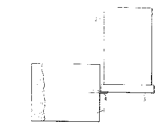
Figure 1 shows a top view of the inventive micro-
strip-to-waveguide transition. The stripline center
conductor 1 is connected to the low noise amplifier
(LNA) circuit 3, which is mounted on an LNA mounting
block 2, via a gold ribbon connect 4. The LNA circuit
substrate, which is made of alumina, is 10 mils thick.
;
- ' ' ' - .
~7~1
The stripline center conductor 1 is approximately 212
mils wide in this embodiment, in order to achieve a 50
n characteristic impedance, with a ground plane spacing
of 160 mils (see Figure 3). An air gap of approximately
~ mils exists between the LNA mounting block 2 and the
end of the stripline 1. An air gap of approximately 2
mils exists between the end of the alumina substrate and
the end of the stripline 1. The gold ribbon 4, which is
approximately 5 mils wide, joins the stripline 1 to the
microstrip 6 on the LNA circuit 3 (Figure 2) across the
small air gap. In so doing, the ribbon 4 rotates
through a 90 angle so that it lies flat on both the
stripline center conductor 1 and the microstrip 6.
While Figure 1 shows the ribbon 4 lying flat on the
stripline center conductor 1, Figure 2 shows the effect
of the 90~ rotation, and thus shows the ribbon 4 lying
flat on the microstrip 6.
In Figure 3, a printed circuit antenna includes a
ground plane 10, a power divider network 20 and a radia-
ting element array 30 comprised of a plurality of radia-
ting elements (not shown). Individual elements of the
power divider network 20 feed respective ones of the
radiating elements. A low noise amplifier circuit 100,
whicb may for example be a two-stage amplifier, is
mounted on a metal block 110 which extends between the
ground plane 10 and the radiating element array 30 to
provide a low resistance connection. The radiating
ele~ent array 30 constitutes the second ground plane of
the antenna; thus, the metal block 110 extends between
the two ground planes. An example of such an amplifier
is shown in Figure 5.
Between the power divider network 20 and the micro-
strip input 140 is a stripline-to-microstrip transition
130. As seen in Figures 1 and 2, a stripline center
conductor 150 is provided on either side of the block
i
2~
100. The conductor 150 is connected to the amplifier
circuit 100 by the stripline-to-microstrip transition
130. The center conduc~or 150 and the microstrip input
140 and output 145 are separated by approximately 10
mils in the illustrated embodiment, and are connected
together by a gold bond wire.
The gold bond is necessary because a DC connection,
is required on the RF output for biasing purposes, bet-
ween the amplifier circuit 100 and the stripline conduc-
tor 150. Preferably the bond is a ribbon bond, such asthat used in microcircuit assembly, wherein the wire is
approximately 5 mils wide and 1-2 mils thick. The
stripline and microstrip transmission sections are
impedance matched. The circuit 100 itself is configured
so as to be self~biased, such that a single positive
voltage is applied at t~e output as a bias, and positive
and negative voltages are generated from that as neces-
sary. A high electron mobility transistor (HEMT~ may be
provided at the front end of the circuit to achieve the
low noise characteristic.
With the foregoing construction, the vertical metal
wall of the carrier block 110 forms a termination of the
stripline transmission mode, in which the electric
fields are oriented vertically between tha two ground
planes comprising the ground plane 10 and the radiating
element array 30. In the actual transition region, the
electric fi~ld of the stripline mode is rotated by 90
to the microstrip mode, since the microstrip circuit
itself is oriented vertically. Figure 4 shows the
relative 90 orientation between the plane of the strip-
line center conductor 150 and the microstrip circuit
more clearly. The vertical orientation of the amplifier
circuit 100 with respect to the power divider netw~rk
makes it possible to take advantage of the symmetry of
the electric ~ield in a stripline transmission mode, and
2~70~1
avoids the complicated structure of USP 4,862,120. The
vertical orientation of the amplifier circuit "folds"
the upper portions of the field down, and also "folds"
the lower portions of the field up, to yield the
microstrip electric field configuration.
As in copending Application No. 07/210,433, in
order to have the LNA block mounted on the radiating
element array, it is necessary to sacrifice certain ones
of the radiating elements which otherwise might be put
on the array. Since the elements may be weighted
appropriately, the elements to be sacrificed may be
selected so as to minimize the effect on performance of
the antenna. For example, elements near the center of
the antenna may be sacrificed by replacing the power
divider elements which would excite them by the LNA
block.
Figure 5 is a schematic of one example of an integ-
rated LNA circuit. In this particular example, the
first and second stage devices are self-biased, and the
single bias voltage is brought in through the RF output
port.
Figure 6 shows a measurement of the stripline test
fixture containing no microstrip circuit. Figure 6 was
provided to obtain a baseline measurement to character-
ize the return loss and insertion 1088 of the externalRF connectors and a lenqth of stripline between them.
Figure 7 shows the same measurement, but now with
a 0.260" length of 50 ohm microstrip transmission line
on a 10 mil thick alumina substrate inserted on a
carrier block in the middle. The extra loss shown in
this measurement arises primarily from the length of the
microstrip line, and the two stripline-to-microstrip
transitions at either end. After taking the inherent
microstrip losses into account, it is found that the
.. . . . .
,,
.
2 ~
transition loss itself is less than 0.1 dB. This result
is associated with a return loss of approximately 17 dB.
Figures 8-10 show that the energy in the stripline
mode is coupled primarily to a microstrip mode by the
transition structure.
While the invention has been described in detail
with reference to a preferred embodiment, various modi-
fications within the spirit of the invention will be
apparent to those of workin~ skill in this technical
field. Accordingly, the invention should be considered
as limited only by the scope of the appended claims.