Note : Les descriptions sont présentées dans la langue officielle dans laquelle elles ont été soumises.
2Q67019
~X'l ~ NALLY MODULATED LASER SOURCE
FOR ARRAY ILLUMINATION
Back~ l o.~l-J of the Invenffon
Technical Field
The present invention relates to an optical power source for array
illumination and, more particularly, to an externally modulated laser configuration.
Description of the Prior Art
Many advanced photonic systems such as optical computing and free-
space photonic switching are based upon arrays of symmetric self-electrooptic effect
10 devices (S-SEEDs). In these systems, the S-SEEDs function as detectors, logicelements, or modulators. Each system relies on arrays of light beams (modulated by
the S-SEED arrays) to transmit information between components of the system. Onemethod for producing the required light beam array is discussed in an article entitled
"Binary phase gratings generating even numbered spot arrays" by R. L. Morrison et
15 al. appearing in the 1989 Technical Digest of the Optical Society of America,Annual Meeting (Vol. 18). The Morrison et al. article describes the beam array
generator as comprising a laser diode source and a spot array generator mech~ni~m,
such as a grating and appropliate lensing. In operation, a collim~ting lens is coupled
to the output of the laser diode, followed by a grating for producing a diffraction
20 pattern related to the size and periodicity of the grating, and a Fourier transform lens
disposed a focal length above the plane associated with the location of the spot array
at the output of the grating. The optical Fourier transform lens functions to change
the wavelength-dependent diffraction pattern into a spatial array (one- or two-
dimensional) of beams, or spots.
Unfortunately, the above-described array generator mechanism requires
stringent tolerances on the laser wavelength, since the spatial displacement of the
light spots is a function of wavelength. For example, if the wavelength is too short
or too long, the spot spacing is either reduced or expanded, respectively, such that
extreme spots are no longer aligned with the underlying photosensitive device (e.g.,
30 S-SEED, 1- or 2-dimensional opto-electronic integrated circuits, photodiodes, etc.).
As array size grows, wavelength control becomes more critical. Additionally, thephoto-sensitive area of a SEED is concentrated within each cell to improve its
performance. Therefore, the beam array must not only be wavelength-controlled, but
physically aligned within the photo-sensitive area of the receiving device.
20670 1 q
-- 2 --
- As photonic-based systems increase in size and speed, the need for
higher power sources grows accordingly. In particular, the operating speed of a
digital system is determined by the energy required to switch the state of an
individual logic device and the capacity of the power supply. One such digital
5 system may comprise a photonic switch capable of handling over a thousand
channels modulated at about 100MHz (on each channel). Such a system may
comprise several modules with at least one S-SEED devoted to each channel. Givena switching energy of approximately one pJ and an optical efficiency of about 10%
(for relaying the light from the laser to the S-SEED array and then on to the next
10 module), a laser of about 1000mW power would be required for each module.
A need remains in the art, therefore, for a light source capable of
generating a spot array which is stable with wavelength and provides sufficient
power for photonic system applications.
Summary of the Invention
The need remaining in the prior art is addressed by the present invention
which relates to an optical power source and, more particularly, to an externally
modulated laser configuration.
In accordance with one aspect of the invention there is provided an
optical source comprising a semiconductor optical gain medium including a
20 reflective rear facet and a transmissive front facet for generating a coherent optical
signal; a partially reflecting mirror element aligned with the transmissive front facet
of said optical gain medium and physically separated therefrom to forrn an externally
modulated laser which includes an optical cavity; a diffraction grating transversely
disposed to receive the optical signal from the transmissive front facet of said gain
25 medium and optically aligned with the partially reflecting mirror so as to form a
plurality of diffracted optical beams as an output of the optical source; first
collimating lensing means disposed between the optical gain medium and the
diffraction grating for collimating the coherent optical signal generated by said gain
medium; Fourier transform lensing means disposed between the diffraction grating30 and the partially reflecting mirror for providing optical signal coupling therebetween;
and second collimating lensing means disposed beyond the partially reflecting mirror
element for collimating the optical signal generated by said partially reflecting mirror
element.
~'
.,.~
- 2a- 20670 1 ~
In accordance with another aspect of the invention there is provided in a
photonic switching system utilizing an array of photosensitive devices to control
switching between logic states of an associate array of logic elements, the photonic
switching system comprises means for génerating an array of optical beams, said
5 optical beams associated with said array of photosensitive devices in an one-to-one
relationship such that each optical beam impinges a separate photosensitive device,
the generator means comprising a semiconductor optical gain medium including a
reflective rear facet and a transmissive front facet, the front facet including a
relatively wide active region for generating a coherent optical signal; a partially
10 reflecting mirror aligned with the transmissive front facet of said optical gain
medium and physically separated therefrom to form an externally modulated laser
which includes an optical cavity; a diffraction grating transversely disposed toreceive the optical signal from the gain medium and optically aligned with the
partially reflecting mirror element to form the array of optical beams as an output of
15 the generator means.
Wavelength stability may be provided in accordance with the teachings
of the present invention by utilizing a control element positioned beyond the output
of the diffraction grating. The control element comprises an array of transparent
regions (positioned to intercept the array of diffracted beams), with non-reflective
20 (e.g., absorbing) material surrounding the transparent regions. If the wavelength of
the gain medium drifts out of the desired range, the size of the beam array (i.e.,
separation between beams) will expand (wavelength increase) or contract
(wavelength decrease). The wavelength shift results in increased energy being
intercepted by the non-reflective material. The result is that insufficient optical
25 power is coupled back into the gain medium to support stimulated emission.
Therefore, optical wavelength stability is attained for the situation where the
stimulated light matches the predetermined system wavelength.
2~6~als
Various other features and advantages of the present invention will
become apparent during the course of the following discussion and by reference to
the accompanying drawings.
Brief Des~ ,lion of ~e Drawin~
S Referring now to the drawings,
FIG. 1 illustrates an exemplary externally modulated spot array
generator formed in accordance with the present invention;
FIG. 2 illustrates an ~ltern~tive embodiment of the present invention
where the diffraction grating and partially reflecting mirror are combined in to a
10 single component;
FIGs. 3-5 illustrate the wavelength-dependent nature of the spacing
between spots of a generated optical beam array,
FIG. 6 illustrates an exemplary arrangement of the present invention
including a wavelength control element for providing stability of the signal
15 generated by the optical gain medium; and
FIG. 7 illustrates an exemplary altered-intensity spot beam array which
may provide greater wavelength control selectivity in accordance with the teachings
of the present invention.
Detailed Description
To obtain high power (e.g., > lOOmW) from semiconductor laser diodes,
broad stripe and broad area devices have been used, due to their wide (e..g, > 50
,u m) current injection stripes which result in a large active volume. In addition, the
wide stripe reduces the power per unit area on the laser facet, thereby increasing the
total optical power which may impinge the facet before damage occurs. However,
25 the stripe dimension also allows for multiple transverse modes to exist. To remedy
this situation, a laser diode may be coupled to an external cavity which consists of a
lens system and partially reflecting mirror. With proper coating of the diode facets,
the external cavity arrangement is capable of providing filtering of the unwanted
transverse modes.
In accordance with the teachings of the present invention, an external
cavity laser may be configured to generate an array of beams, or spots, suitable as a
light source for array applications such as, but not limited to, optical computing or
photonic switching. FIG. 1 illustrates an exemplary spot array generator 10 of the
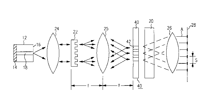
present invention. Generator 10 comprises a semiconductor gain medium 12
35 including a reflective rear facet 14 and an anti-reflective (AR)-coated front facet 16.
A relatively wide active stripe 18 is formed within medium 12 such that light is
2~6701~
emitted in the indicated direction. It is to be understood that the drawing of FIG. 1
(as well as the following illustrations) is not to scale and, in fact, has been enlarged
for the sake of explanation. Generator 10 further includes, at the output thereof, a
partially reflecting mirror element 20 which is designed to allow a predetermined
5 portion (e.g., 10%) of the light impinging its surface to pass therethrough. The
remAinder of the light energy is reflected back through generator 10 so as to re-enter
gain medium 12. The combination of partially reflecting mirror 20 and reflectiverear facet 14 thus form a cavity which is capable of supporting the desired laser
mode.
In accordance with the teachings of the present invention, a diffraction
grating (cont~ining a predetermined pattern as will be discussed below) is utili~ed to
generate the desired spot array pattern, where the pattern may either be one-
dimensional (e.g., a single row or line of spots) or two-dimensional (e.g., a matrix of
spots). Referring to FIG. 1, a diffraction grating 22 is illustrated as being disposed
15 between gain medium 12 and partially reflecting mirror 20. Generator 10 further
comprises a collimAting lens 24 positioned between gain medium 12 and grating 22,
and a second lens 25 disposed between grating 22 and partially reflecting element 20,
where lens 25 is positioned a focal length f between elements 22 and 20. A finalimAging lens 26 is positioned beyond partially reflecting mirror 20 and functions to
20 image a collimated beam array onto an array of photosensitive devices 28.
Generator 10 is initiated by biasing gain medium 12 (not shown) such
that an optical signal will be emitted from active region 18. This light from gain
medium 12 is then collimated by lens 24 and the collimated beam impinges grating22. Diffraction grating 22 is composed of a periodic replication of either a one- or
25 two-dimensional pattern across the surface of a transparent substrate. The pattern's
periodicity produces a regular spacing of grating orders, while the pattern itself
determines the relative order intensities (i.e., the energy coupled into the various
spots). The grating may be formed either by etching the substrate or depositing a
material onto the substrate surface. A complete description of an exemplary
30 diffraction grating, referred to in the art as a "DammAnn grating", may be found in a
article entitled "High-efficiency in-line multiple imaging by multiple phase
holograms", by H. DAmmAnn et al. appearing in Optical Communications, Vol. 3,
1971, pp. 312-315.
The array of diffracted beams formed by grating 22 subsequently passes
35 through lens 25 which performs an optical Fourier transform so as to change the
frequency-based array of beams into a spatially-based array of beams. The spatial
~06~019
array then impinges partially reflecting mirror element 20 where, as indicated by the
dotted lines, a fraction of the energy passes therethrough unimpeded (e.g., 10%). The
propagating spot beam array A is then collimated by im~ging lens 26 and
subsequently focused onto the array of optically-sensitive devices 28, such as the
5 symmetric self-electrooptic effect devices (S-SEEDs) mentioned above. It is to be
understood that the spot array generator of the present invention is suitable for use
with virtually any array of photosensitive devices. The description of S-SEEDs
throughout the course of the following discussion is considered to be exemplary only
and not to preclude or limit the scope of the present invention. As indicated by the
10 double arrows in FIG. 1, the remaining light energy reflected by mirror element 20
propagates back through the system and re-enters gain medium 12. Since the lenses
and the diffraction grating are reciprocal elements, the various rays will converge at
laser diode 12 so as to re-enter active region 18 and again be reflected by rear facet
14 to m~int~in the lasing action.
An alternative arrangement of the present invention where the grating
and partially reflecting mirror are combined into a single element is illustrated in
FIG. 2. As shown, generator 30 of FM. 2 comprises a laser diode 12 essentially
identical to that described above in association with FIG. 1. A similar lens 24 is
utilizes to collimate the output beam from active region 18 of laser diode 12. The
20 collimated beam next impinges reflective grating element 32, as shown in FIG. 2,
which functions to reflect a portion (e.g., 80-90%) of the collimated beam and
transmit the remainder. As shown in FIG. 2, element 32 comprises a partially
reflecting surface 34 which redirects a portion of the collimated beam back through
lens 24 and into device 12 to m~int~in the stimulated emission. The tr~nsmitted
25 portion of the collimated beam is subsequently diffracted by a grating feature 36
formed on the opposing surface 38 of element 32. The generator array of beams A is
subsequently collimated by imaging lens 26 and focused onto the optically sensitive
array of devices 28, as with the arrangement of FIG. 1. Alternatively, the positions of
reflecting surface 34 and grating feature 36 may be reversed so that the collimated
30 beam from lens 24 is first diffracted and then reflected.
Regardless of the embodiment employed, a critical aspect of the
invention is the ability to achieve alignment between the spot array A and the array
of devices 28. In free-space optical logic system applications, the spot array is
designed to contain a central region with orders of uniform intensities. It is highly
35 desirable to couple a substantial fraction of the total intensity into these orders. The
array can be composed of either an odd or even number of spots, where both types of
2067Q19
- 6 -
arrays form regularly-spaced arrays of spots. However, the even-numbered spot
array contains suppressed (or zero intensity) orders interlaced with the high intensity
spots. An exemplary relatively simple grating which may be used in accordance
with the present invention is the two-level, or binary phase grating (BPG). The
S binary phase grating creates a set of N spots in an odd-numbered array using apattern with approximately N/2 phase transitions. The even-numbered design
requires approximately twice as many transitions, since the suppressed orders require
additional parameters in the design process. For even-numbered designs to achieve
an equivalent spot spacing, the order spacing must be halved, leading to a doubling
10 of the period. The binary phase grating is designed using optimization techniques
that measure performance based on scalar diffraction theory and may be fabricated
suing standard micro-lithography and etching procedures. An exemplary one-
dimensional BPG has a diffractive efficiency (the fraction of energy coupled into the
desired central orders) in the range of about 70-80% for moderately sized arrays.
15 The rem~ining energy is dispersed into higher order spots. FIG. 3 illustrates an
exemplary one-dimensional spot array A which is essentially aligned with an
underlying array of optically sensitive devices 28. In the case where alignment is
achieved, the wavelength ~ of the spot array generator is essenti~lly identical to the
calculated wavelength ~0 required for the predetermined spacing S of devices 28,20 where
S = 2 (~f),
for even-numbered designs, with f being defined as the focal length of lens 25 and P
as the pitch of grating 22. For odd-numbered design~, the factor of two is dropped.
This wavelength sensitivity becomes critically important in a large spot array since
25 the overall size, which is the sum of all spot spacings, must match a fixed size
photonic device array layout. It is often advantageous (and for even-numbered
gratings, necessary) to design the grating such that light traversing the two separate
regions differs by a phase shift of ~. As a result of this requirement, any portion of a
plane wave that experiences two separate ~ phase shifts would behave equivalently
30 to experiencing no phase shift. The 7~ shift allows for the combination of two
orthogonally oriented independent solutions to from a two-dimensional structure and
still m~int~in a binary level design.
Referring to FIG. 4, if the generator wavelength ~ is (or becomes)
shorter than the calculated wavelength ~O required for the particular spot spacing S,
35 spot array A will become misaligned with devices 28 in the manner illustrated in the
~Q~Ol9
drawing. In contrast, FIG. 5 illustrates the situation where the wavelength ~ of the
generator is (or becomes) longer than the desired system wavelength ~0. In either
case, it is clear that if the generator wavelength is allowed to drift too far from the
desired value ~0, insufficient light energy will be coupled into the optically sensitive
5 devices. The ability to control the wavelength of such an array generator, therefore,
is critical to the performance of the system.
The movement of the spots as a function of wavelength variation can be
utiliæd in accordance with the teachings of the present invention to produce a
passive wavelength control arrangement. FIG. 6 illustrates an exemplary
10 arrangement of the present invention (similar to that discussed above in association
with F~G. 1) including a wavelength control element 40 which may be used in
accordance with the teachings of the present invention to provide passive wavelength
control. As shown, element 40 comprises a plurality of transparent regions 42 and a
non-reflective (e.g., absorbing or attenuating) region 44 formed to surround the15 plurality of transparent regions 42. Referring to FIG. 6, transparent regions 42 are
disposed so as to align with the various beams forming the spot array generated by
diffracting element 22 when the generator wavelength ~ is essentially equal to the
predetermined value ~0 required for the predetermined spot spacing S. ~ssllming the
system wavelength is at the desired value, therefore, the diffracted array formed by
20 grating 22 will pass through transparent regions 42 unimpeded and enter partially
reflecting element 20. As the wavelength begins to drift (in either direction),
however, the spot array will physically shift (as illustrated in FIGs. 4 and 5) such
that a significant portion of the optical energy will impinge non-reflective region 44
of element 40. The attenuation (i.e., non-reflection) of the signal power within25 region 44, therefore, results in a decreasing amount of energy being returned to gain
medium 12 such that stimulated emission cannot be maintained. An optical power
monitor can be used, therefore, to modify the laser bias current in response to the
drop in reflected power so as to stabiliæ the wavelength of the generator.
Although the above arrangement is suitable for most applications, there
30 may exist systems which require an enhanced wavelength sensitivity. For example,
in extremely large arrays (i.e., hundreds of elements), the outermost beam spots and
associated optically sensitive elements may become mic~lignPd long before any
noticeable change in reflected signal power is achieved, since these elements account
for only a fraction of the total signal intensity. Thus, an alternative wavelength
35 control arrangement may be utiliæd in this case. In particular, a diffraction grating
may be modified so that an increased signal intensity is directed to the outermost
~G67~19
spots, with a highly reflective mirror (perhaps 95-100% instead of 80%) used to
return the beams back through the generator. FIG. 7 illustrates an altered spot array
suitable for this purpose where the diffraction grating has been altered such that
spots 50,52 of a beam array 54 are generated to provide an increased intensity over
5 the intcrn~l spots 56. Highly reflective mirror elements 60,62 are illustrated as
aligned with spots 50 and 52, respectively, so as to couple an increased percentage of
their energy back into the generator. Therefore, wavelength drift resulting in
mi.~lignment of spots 50,52 (shown in phantom in FIG. 7) will be detectable withthe illustrated altered beam pattern. In fact, spots 50, 52 may be used solely for
10 wavelength control purposes. In this case, spots 50, 52 would not be associated with
any underlying optically sensidve devices and approximately 100% of the impinging
optical signal would be reflected back into the spot array generator.