Note : Les descriptions sont présentées dans la langue officielle dans laquelle elles ont été soumises.
2~33~
'.`'.. `~91/05306 PCT/AU90/0047~ -
~,~ ..~'
ELECTRO-ACTIVE C~ADLE CI~CUITS ~OR THE DETECTION OF
ACCESS O~ PENETRATIO~
The present lnvention relates to the protection of information stored
wlthin electronic c~rcuits and in partlcular to the protection o~ stored
data from a hardware thief or hacker
The protectlon will be achieved by the use of an electroactlve Cradle
clrcuit. A cradle i5 defined here as a framework for support or
protection (refer Collins Australlan Dictionary of the English Lancuage
1981).
BACKGROUND ART
With the development of extensive computerised memory and tne ~eed
for conf~dentlallty of data stored wlthln that memory there have been
developed a number of methods of preventing the theft o that secret
tnformation. Traditlonally computer software has been protected bv means
of encryption and decryptlon programming. Also encrypt10n and decryption
hardware elements have been incorporated into speclfic electronic packages
to perform data protection under software control. With the development of
sultable algortthms and keys contained in alterable memory it has been
possible to successfully protect data from an information thief or hacker
who attempts to access that data by 50ftware means
However these known methods offer little securlty from a hardware
hacker who obtains electronic information through physical access to such
electronic circuitry. Electronic information or data comprom~se can occur
by drilling through existing encapsulants of electronic circultry so 2S to
access data and/or address buses. These may be located by X-ray
radiography and/or ultrasonic techniques. Alternatively employmen. o
thermal solvent acid simple mechanical scraping or mechanical fracture
methods can be used to expose the data and/or address buses assoc~ated with
the alterable memory.
Such alterable memory can comprise EPROM E2PROM RAM DRAM and
PROM. Some devices though having some protection permit learning of the
me~hodology so that a thief can steal ore device and therefore know the
next. However the hardware hacker can _~tain no information from a
severed communication channel external to the device due to so~tware
methods such as encryption and authentication procedures. Once the
information thief or hacker has gained the knowledge of the authentication
procedures and the data codes necessary one could make use of thi 5
information to advantage. These types of security problems are
particularly relevant to financial institutions which use security sysiem
SU~STITUTE SHEET
. . ' '- ' . ' .. : . '
wo 91/05306 2 ~ 7 ~ 3 ~ ~ pcr/Au9o/oo475
to secure computerised transfer of funds the value of whlch is several
m~ ons of dollars per hour. In the case of a financial lnstitution once
an information thief or hacker has gained the authentication procedure and
the necessary data codes ill~clt funds transfer could occur and the
transfer would appear as a legal and authorised transaction. As such~ any
secur~ty compromise could result in the flnancial lnstitution incurring . .
fraud losses loss of integrlty recover)l costs adverse publicity and loss
of commercial confidence.
US Patents 4 593 384; 4 691 350; 4 807 284 and 4 811 288 cover the
area of secur~ng stored data us~ng a device that physically surrounds the
circuit board being protected.
The secur~ .y device in the 4 paten s i; comp.ised of:
1) a number of ceram~c components that form a box that surrounds the
circuit board. Ceramic is used because of its chemical resistance
2~ w~thin the ceramic components are a number of conductive epoxy
paths and sheets through which a hacker would penetrate ~f attempted
pénetration occurred.
3) in certain embodiments these conductive paths may also be
connected vla thtn wires that pass through the circuit board
4) in a further embodiment thin nickel/gold layers were deposited
onto the inslde face of the ceram~c housing. These layers were then etched
to form parallel gold conductive paths (10-2511m thick with same spacing)
S) by shorting or breaking the conductive paths or sheets a sense
circuit w~ll generate a low voltage that sets the RESET on the memory to be
protected and
6) a low temperature sensor (an unbalanced circuit) will also
generate a low voltage jc the temperature falls below -25~. This ensures
that if an attempt is made to freeze the memory below -90C in order to
bypass the security device the memory will be destroyed and thus protected.
US Patent 4 783 801 is for a security device to protect a circuit
board. The security device is comprised of:
1) a housing in which one or more detectors may be situated. These
detectors being vibration detectors thermometers microphones or
conductive paths that are shorted or broken upon penetration and
2) the interface circuitry includes a clock arrangement that turns on
the detectors for short intervals (ie:lOms every second) leading to a
saving of upto 99X of the battery power and ensuring that the battery does
not have to be periodically replaced. The interface can also decide whether
~ ., ;- - ^ .~ , , -: . .
- , ~ , . . ..................... . . .
.
W o 91/05306 _ 3 ~ O ~ 7 3 3 1 . PCT/AUgo/00475
o destroy the memory using ma~orlty information from`lts dete~ctors. (ie: 3
detectors out of 5 say yes the- the interface corruDts the memory).
US Patent 4 860 35~ rela s to a securlty devlce for a circuit board.
The securlty devlce is comprised of: ~ -
1) very thin lnsulated Nichrome wire is wrapped in ver~ tight coils
around the circuit to be protected The circuit and enclosing wire is
potted wlthin an opaque cross-linked filled epoxy. The filler in the epoxy
~s alumina or silica which makes the epoxy difficult to mach~ne
2) if penetration is attempted the wires are shorted or broken the
interface circuit will sense this and destroy the memory and
3) the wire ~s wrapped as several strands which enhances sensitivtty
to shorts and reduces EMI pickup due t~ cancellatlon. The ~ire wrap also
forms an EM shield.
Such techniques have been proposed to provide protection against such
compromise or ingress. However these methods are complex and integrated
with the device to be protected thus making that device irreparable.
Overall thls invention is based on different materials and methods which ~:
wlll offer protection to data system(s) including such memory devices
indicated below whilst permitting economic repairability and therefore
recycling of that device.
Various methods are known to prevent or frustrate transmisston of
x-rays and other short wavelength radiation.
AU 41240/78 teaches that barium titanate barium fluoride and lead
sulfate can be added to an organo polysiloxane resin for X-ray shielding
applications.
AU 17377/B8 teaches that barytes can be added to Plaster-of-paris up
to 60% by weight with Plaster-of-paris 35% by weight and other fillers
sealers and hardeners comprising the other 5% by weight. It is envisaged
for use as an economic alternative to lead in floor wall and ceiling
shielding in hospitals.
W089/09472 relates to oxides hydroxides and salts of bismuth loaded
into polyethylene at weight fractions ranging from 30 to 80 X for use as
flexible protection in surgical clothing such as gloves aprons boots and
overalls.
GB 1 575 527 describes X-ray opaque sursical sponges using elastomers
(ie: polyisobutylene PVC and copolymers of VA and VC) loaded with 40 to
90 % weight fraction barium sulphate.
Such methods can be used to enhance the devices of the present
-. . . ~ . . . . : . . . ~ .!
: . ": ,: ~ . :: '. , '' '' ' '' ' .
WO 91/05306 ~ 4 PCr/AU90/0047S
invention . S~o ~7 3 ~ ~
CISCLOSURE O; T~ INVENT-IO~
It is an object of the present invention to substantially overcome or
ameliorate, the abovementioned d~fficultles through prov~sion of one or
more transducers, which may be used in association with an encapsulant or
housing which protects electronlc circuit(s) that contain data required to
be protected from the effects of hardware hacking. In certain applications
both the transducer and the encapsulant or housing will be capable of being
employed separately to provlde protection. For example the transducer
components could be supported vla a suitable alternative support while the
encapsulant could be used to provide a X-ray attenuating mechanical barrier
to frustrate attempted penetration. ..
In accordance wlth one aspect of the present invention, there is
disclosed an electronic clrcult or dev~ce protected from tamper andlor
theft of informat~on conta~ned thereln, compr~sing sald circuit, a
transducer capable of generating a voltage, detection means to detect said
voltage, and protect~on means associated therewith to destroy and/or alter
said c~rcuit, device andlor information andlor record said voltage,
characterlzed in that said transducer is a polymeric pressurelvoltage
andlor temperaturelvoltage transducer associated with said detection means
such that on alteration of pressure or temperature applied to said
transducer beyond pre-set lim~ts, sald vo!tage ~s sensed by said detection
means thereby activating said pro~ect~on means.
In another aspect, the invention provides a method of protecting an
electron~c circuit or device or ~nformation stored therein from tamper
andlor theft that occurs through an examination of said circuit or device,
said method comprising providing a polymeric pressure/voltage andlor
temperaturelvoltage transducer capable of generating a voltage adjacen.
said circuit or dev~ce, said transducer being associated with detection
means to detect said voltage, and protection means assoc~ated with said
detection means, such that on alteration o~ pressure or temperature applied
to said transducer beyond pre-set limits, said voltage is sensed by said
detection means thereby activating said protection means to destroy andlor
alter said circuit, device andlor information andlor record said voltage.
The circuits or devices which may be protected in accordance with the
present invention may include signal processing circuits,
encryption/decryption circuits, alterable memories and the like. The
circuits or devices of the invention can be protected by a single
W o 91/05306 5 _ 2 0 ~ 7 3 ~1 PCT/AU90/0047~
transducer which may be a pressure/voltage transducer or a
temperature/voltage transducer. It is preferred that both a
pressure/voltage transducer and a temperature/voltage transducer be used.
The transducer may be arranged to fully cover or enclose the circuit
so that any attempt to access the combination is required to pass through
the transducer.
The detection means may be located within or adjacent to the
transducer and preferably comprises at least two electrodes associated with
the circult. One of the electrodes may be earth. In order to disguise the
transduce~ from examination by electromagnetic radiation and/or acoustics
lt is preferred that the electrodes are non-metallic. For some
appllcatlons the detectlon means may lnclude an associated electronic
circuit such as an amplifier which may be located within or adjacent the
transducer.
The transducer may contain an external or integrated switching means
to prevent inadvertent activation of the protection means. It is preferred
that a destructible conducting element may be provided adjacent the
transdùcer to short-circuit the electrodes to prevent activation of the
protection means prior to destruction of the conducting element. In
general the protection means will be activated only when the output of the
detection means exceeds preset limits.
In a preferred embodiment of the invention the transducer output is
disabled by connection of the detection means by metallic or non-metallic
electrical conductors to a gating circuit or device which prevents the
active output of the transdùcer being transmitted to the detector. The
gating circuit can be controlled by elements of metallic or non-metallic
components of a bridging circuit. The conditions of the bridging circuit
can be altered by breaking due to penetration of one or more bridge
elements.
In an alternate preferred embodiment of tn-. invention the transducer
is disabled by having the electrodes of the det~ction means connected by
metallic or non-metallic conductors thus preventing the buildup Oc charge
and hence prevent spuriou~ r unwanted generation of voltage signals due to
normal vibration or temperature variations. The connection may be affected
in such a way so as to be broken upon any penetration through to the
transducer. On breaking of the connection the transducer is immed~ately
enabled to generate a voltage due to an attempted penetration.
Where it is desired to protect a circuit or device fron the effects
of aggressive chemicals such as solvents oxidising agents and/or reducing
-
~, . , . - . . .
.. .. . . ,~ ~.,, .. . ~ . -
W O 91/05306 2 Q ~ 7 3 ~ ~ 6 - PCT/AU90/00475
agents, the transducer can De mod~fied so as to generate a vo~tage on
contact with the aggressive chemical. Alternat-el~, a further chemica~
sensing/voltage transducer may be provided as part of the circuit or
aevice. Such a further transducer can be constructed from a conducting --
polymer having groups or radicals incorporated therein which react with the
aggressive chemical or from a piezo-electric polymer coated with a material -
which reacts with such aggressive cnemicals. ~ ,
For some applications, it may be desirable to make the circui , or
transducer unable to be examined by electromagnetic radiation or acoustics
to prevent/frustrate examination of the circult or parts thereof with an
acoustics or electromagnetic radlation resistant encapsulating element.
The element may also be formulated to be resistant to agressive chemicals.
It ls preferred that the encapsulating element is formulated to achieve the
maximum electromagnetic and/or acoustic and/or chemical attenuation whilst
remaining both non-corrosive to contained components and electrically
insulating. For example, the encapsulating element can be formulated with
high atomtc number compounds in a supporting material such as epoxy or
polyurethane,in quantities up to and beyond 80% w/w. For some
applicatiQns, the encapsulating element may be formulated with small
quantities of metal arranged throughout the element to further disguise the
configuration of the circuit or device or part thereof, The encapsulating
element may also include ceramic materials to further prevent/frustrate
mechantcal ingress and/or an electrical tnsulation layer.
To those skilled in the art, the well catalogued cryogenic threat of
rapid coollng, to temperatures below -90~C, of circuitry to ensure
preservation of data, may be overcome by the inclusion of temperature
sensors working in conjunction with the crad1e and/or its signal processing
circuitry. The thresholds of these sensors would be determined by the
operating environment of the device being protected. In addition, to
ensure the preservation of the piezoelectric effect in the piezoelectric
sensing material, a high temperature sensing element may be included as
part of the signal processing circuitry.
Conventional devices such as silicon integrated circuits,
transistors, resistors and capacitors in addition to equivalent devices
made from electroactive polymers, will as a circuit receive the detection
signal, perform any necessary signal processing and output to the
associated circuit being protected, a predetermined signal in response to
the intrusion or investigation.
.
..... ,. ~ . . . . . , , , , ~ . .
: :, . ,
- ~ . .
. . . . ..
~ . . . . : .
w O 91/05306 2 0 6 7 3 3 ~ PCT/AU90/0Q47~ ~
Ihe signal processing which might typically ;be,performed b~ the
polvmer cradle circuits in conjunction with existing conventional
electronic devices would be amplification, comparison~ clipPing, filtering
as well as known logic functions. Signal processing could be carried out
as an integral Part of the cradle aevice or separately bv the electronics
board belng protected. Power, lf required, could be derived from tne
application electronics board or be supplied from an auxiliary source, for
example a lithium cell. The decision whether or not a dead or decaying
power soùrce condltion causes circuit in~tiation (eg: failsafe) may be left
up to the apPlication subject to that protection.
Polymers suitable for processing lnto pressure/voltage and
temperature/voltage .ransducers are generally halogen con.aining polymer5
which are ava~lable commercially. Polv(vinylidene fluoride),
poly(vinylidene fluoride-trifluoroethylene), polytetrafluoroethylene,
polyvlnyl chloride, polyvinyl fluoride or copolymers thereof are examples
of the polymers available. In order to achieve higher piezoelectric and
pyroelectric activ~ty, these polymers should be stretched and polarized.
The stretching of the polymer, followed by polarization in intense elec ric
ields at elevated temperatures aligns the dipole moments within the film,
producing the desired piezoelectric and pyroelectric effect. In order to
polarize and use these polymers, electrically conducting electrodes can be
deposlted onto the faces of the material, to which electrical conductors
may be connected. It is advantageous for certain applications to utilize
single face electrode connections, achieved by forming separated electrodes
on the one face.
Such piezoelectric and pyroelectric polymers are tough, liahtweight,
flexible and may be formed lnto comple~ shapes suitable for any application.
There is well established use of semi-conducting polymer composites
or compounds which are made by the addition of conducting particles, such
as silver, aluminium or carbon, to a polymer. However these materials
cannot be made to have sufficiently high conductivity for many
applications. There are now available a wide range of relatively new
intrinsic conducting, semiconducting and piezoelectric Dolymers which can
be synthesized in the laboratory, a few o, which are available
commercially. Polyacetylene, poly p-phenylene, polyaniline, polythiophene,
polyquinoline, polypyrrole and polypyrrone are some of the many
intrinsically conducting and semiconducting polymers which can be chosen
for the fabrication of electronic devices and circuits. A wider range of
. . .
!:; . , .. .
',; .
WO 91/05306 PCI/AU90/00475
2067331
sPecific conducti~ities can be obtained than that possible using conducting
polvmer/compound composites. These new electroactive polvmers are also
more suitable for fabricatlon of electronic transaucers. For example,
polypyrrole can be syntheslzed to have a w'de range of conductivity by
aqueous or organ~c electro-chem~str~ using d~fferent concentrations of
sodium p-toluene sulpnonate as the dopant dissolved in the electrolyte.
The deposited film of polypyrrole can be changed in shape by modifyina the
geometry of the anode formed to make a three-dimensional frame wor~. Using
conduct~ng and sem'conducting polymers, a wlde range of polvmer pn
~unctions, transistors, chemsensors and batteries are being researched.
BRI F D-SCRIPTION O, THE DRAWINGS
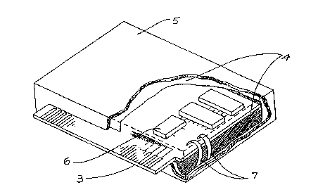
Flg. 1 is a plan vlew of the devlce that embodies the present invention.
Fig. 2 is a cut-away of an example of how the cradle encloses the device to
be protected.
Fig. 3 is a plan view of an example of how the cradle is formed.
Fig. 4 is a schematic example of the signal processing circuitry.
BEST MODES OF CARRYING OUT T~IE INVENTI~N
A preferred embodiment of the present invent;on will now be described
with reference to the drawings that i!lustrate the present invention.
An example of an electronic device which may be protected in
accordance with tne present invention is that of an alterable memory 1 as
earlier described. Generally associated with the alterable memory 1 is a
data encryption/decryption circuit or application specific data processing
device 2 that interfaces the alterable memory 1 with a data connection 3
that provides communication with other devices (not illustrated). Note
that the application specific processing device may exist ~n hard or
software form. An example of such a device as now described would be a
Personal Identification Number (PIN) pad used in automatic telling machines
(ATMs) and electronic funds transfer point of sale (EFTPOS) machines
operated by banks and other financial institutions. In such an example,
the alterable memory 1 would contain a key or a series of keys required for
the encryption processes typically carried out in a Personal Ident;fication
Nu~ber encryption transaction. Access to the key~s) contained within the
alterable memory 1, could enable an information thief to compromise the
system integrity.
~ilJE~ST~TUTE S~!~
.
,
. . .
, .
W 0 91/05306 q _ ~ ~ 6 7 ~ 3 ~ PCT/AU90/00475
The circuit combination of the alterablè memor~ 1 and data
encryption/decryption circuit or applicat~on specif~c device 2 are enclosed
within an electroactive polvmer cradle ~ ~Ref:Figs. 1~ 2 & 3). The
electroactive polymer cradle 4 is interfaced to the circuit combination 1
and 2 via a signal processing circuit 6 utilising metallic or non-metallic
electrical conductors 7. The signal processing circuit 6 (Ref:Fig.4)
comprlses fundamentally of a low power amplifier capable of saturation at
lts output 9 replicating digital conditions and driven by the analog
cradle output. The electroactive polymer cradle 4 covers all three
dimensions of the circuit combination 1 2 6 and 7 such that the data
connection 3 is the only physical connection from outside the cradle 4 to
w~thin the circu~ combinatlon 1 6 and 7. (Ref:Figs 1 & 2). The
polymer cradle 4 may also be enclosed within an encapsulant or housing 5.
The data connect~on 3 can be arranged to exit the encapsulant or housing 5
in the form of connecting p~ns or a cable or leads (not illustrated).
It will be realised by those skilled in the art that an information
thief that obtains that information by accessing through software
techniques would be resisted in any efforts by the encryp~ion/decryption
circùit or application specific processing device 2 and/or any one-way
functions ~OWFs~ therein. As such the alterable memory 1 is safe from
software intervention as previously known in the art
The electroactive polymer cradle 4 comprises electroactive polymer
ctrcuit(s~. The cradle circuit(s) is arranged to fully cover (2D) or
enclose (3D) the circuit combination 1 2 6 and 7 so that any attempts to
hardware access the combination 1 2 6 and 7 are required to pa s through
the electroactive polymer cradle 4.
The electroactive polymer cradle comprisei a variety of polymer
devices linked by polymer or metallic electrical conductors. Some of these
polymer devices are sensing elements chemsensors piezoelectric
transducers and thermal sensing elements. These sensors may be made
sensitive to physlcal and/or chemical ingress to provide stimuli to other
devices located within the cradle. It is also possible that the sensors be
sensitive to investigation by acoustic waves electromagnetic radiation and
particle beams. Once activated by any ingress or destructive investigation
of the cradles the electroactive polymer circui. then emits a signal(s~ in
order to record the event or to initiate the alteration corruption and/or
destruction of the information stored within the alterable memory 1. This
same method can also be adapted to initiate the alteration corruption or
. . . . .. . ~. . . . , ...... -
W 0 91/05306 ' ~ P ~ /AU90/00475
~estruction of th~ ~a~ ~ ~s~ ~ b~ or stored b~ tne encryption/oecryption or
application specific algorithm within the encryption/decryption or
application specific device
The cradle output is normally inactive. Activation would occur as a
result of any one of the aforementioned methods of hardware hacking and
thus negate any criminal ~earning process. For certain applications it is
proposed that the cradle only be sensitive to a destructive penetration or
attack that is being undertaken and not sensitive to external impacts or
v~brations that will occur in everyday use of the types of circuits and
devices that are to be protected. The electroactive polymer cradle 4 would
remain in a switched off mode until an attempted penetration occurred. :.`
To sw~tch off the elec~roactive polymer cradle 4 the electrodes ~
~Ref:Figs. 3 & 4) of the electroactive polymer cradle 4 would be formed in
such a manner that no output can occur. Figure 3 illustrates an example
of the electroactive polymer cradle 4 from which plane electrode material
has been removed to form an electrical pathway. On penetration of the
electroactive polymer cradle 4 the electrode 8 conditions would be
modi ied making the cradle output active.
Alternatively the electrodes of the electroactive polymer cradle 4
could be connected by metallic or non metallic electrical conductors 7 to a
gating clrcuit wh~ch would normally prevent the electroactive polymer
cradle 4 from transmitting its output~s) to the signal processing c1rcui.
6. The conductors could form for example elements or a bridging circuit
which would control the previously mentioned gating circuit. These
conductors would be affected in such a way that any penetration through to
the electroactive polymer cradle 4 would alter these conductors and
influence the gating circuit.
The encapsulant or housing 5 may surround the etectroactive polymer
cradle circuit 4 its purpose being three-fold:
a) to mechanically support and contain the electroactive polymer
cradle circuit 4 and the device or circuit being protected.
b) to prevent/frustrate examination or location o the
electroactive polymer cradle circuit 4 and the metallic buses terminals
and ccndu.ting paths of the enclosed electronic devices by X-ray methods
and/or acoustics. It is also possible that the encapsulant or housing 5
could be formulated to preventtfrustrate examination or location by gamma
rays neutron beams and electromagnetic waves.
c) to prevent/frustrate dissolving or swelling in common solvents.
~ C ', ~ C r-~
. .
:. , ~ . . ~ . . - . ,
. .
w o 91/05306 ~ O ~ 7 ~ ~ ~ PCT/AU90/0047~
The encapsulant or housing 5 ~hen necessar.y ~ill be formulated tc
achieve the max~mum poss~ble X-ray attenuation ~h~lst remainlng both
non-corrosive to contalned components and electrically insu~ating. High
atomic number metalllc salts and oxides for example barium and/or lead
salts ~e.g. Barytes and Litharge) would be added to a supporting material
such as epoxy or polyurethane polymers in quantities up to and beyond 80
w/w Small quantities of metal could also be arranged throughout the
encapsulant or housing S to further disguise the actual position of the
contained polymer cradle circuit and device~s) or circuit(s) being
protected.
As an enhancement for certain applications fillers and/or hardeners
would be lncorporated lnto the encaDsulant or housing S to further
prevent/frustrate mechan~cal lngress. In certa~n appl~cat~ons conducting
materials elther metallic or non-metallic would be incorporated into the
encapsulant or housing 5 to provide an electromagnetic radiation shield !~
that could be used for radiation hazard attenuation. When required an
electr~cal insulation layer would also be added to the encapsulant or
housing 5.
INDUSTRIA~ APPLICABI~ITY
The present invention can be applied in general to any type of
comput~ng devlce microprocessor elec~ron~c device storage element and
logic element that contains information that is not to be d1sclosed. Also
it can be used in any circuit or similar device that might be required to
operate or fail in a desired or predetermined manner when subjected to
forces measures or substances constituting intrusion.
The above descrlbed example of protecting keys used in funds transfer
in Personal Identification Number (PI~) pads Electronic Funds ~ransfer -
Point of Sale ~EFTPOS) or general information security is applicable
throughout the financial industry as well as broader uses relating to
electronically stored information.
The present invention also has well placed application in the
defence communications electronics and computing industries. Examples of
possible areas of application are encry~.ion/decryption processes and
devices smart card peripherals and ma ic stripe readers ~MSRs~. -
A further application is in the ection of devices that control
the function of and the arming of exploiives and ordinance.
The present invention offers to users of elec.ronically stored ;~
information a means by which that information can be ;ecurely stored
without the possibility of theft. As such devices protected in accordance
W O 91/05306 2 Q ~ 12 - PCT/AU90/00475
w~th the present ~nvention have applications througnout the financial ano ~ .
defence industries as well as in the general computingJelectronics industrv
The foregoing only descrlbes one embodiment of the present invention -
and further embodiments, obvious to those skilled in the art, can be made
thereto wlthout departing from the scope of the present information.
. ~
' ':, ' ' '