Note : Les descriptions sont présentées dans la langue officielle dans laquelle elles ont été soumises.
WO 91/06114 ~ ~ ~ ~ ~ ~J ;~ PCT/US90/05307
-1-
AN APPARATUS AND METHOD FOR MANUFACTURING
A SCREEN ASSEMBLY FOR A CRT
UTILIZING A GRID-DEVELOPING ELECTRODE
The present invention relates to an apparatus and
method for electrophotographically manufacturing a screen
assembly and, more particularly, to utilization of a arid-
developing electrode for manufacturing a screen assembly
for a color cathode-ray tube (CRT) using dry-powdered,
triboelectrically-charged screen structure materials.
A conventional shadow-mask-type CRT comprises an
evacuated envelope having therein a viewing screen
comprising an array of phosphor elements of three
different emission colors arranged in a cyclic order,
means for producing three convergent electron beams
directed towards the screen, and a color selection
structure or shadow mask comprising a than multi-apertured
sheet of metal precisely disposed between the screen and
the beam-producing means. The apertured metal sheet
shadows the screen, and the differences in incidence
angles permit the transmitted portions of each beam to
selectively excite only phosphor elements of the desired
emission color. A matrix of light-absorptive material
surrounds the phosphor elements.
U.S. Pat. No. 3,475,169, issued to H. G. Lange on
Oct. 25, 1969, discloses a process for electrophoto-
graphically screening color cathode-ray tubes. The inner
surface of the faceplate of the CRT is coated with a
volatilizable conductive material and then overcoated with
a layer of volatilizable photoconductive material. The
photoconductive Layer is then uniformly charged,
selectively exposed with light through the shadow mask to
establish a latent charge image, and developed using a
high molecular weight carrier liquid bearing, in
suspension, a quantity of phosphor particles of a given
WO 91/06114 ~ ~ ~ ~ ~ ~ ~ PCr/US901OS307..
°:;,:;
-2-
emissive color that are selectively deposited onto
suitably charged areas of the photoconductive layer.
The charging, exposing and
deposition processes are repeated for each of the three
color-emissive, i.e., green, blue, and red, phosphors of
the screen.
An improvement in electrophotographic sar~eni~ng is
described in ;7.5. Pat. No. 4,921,767, issued to P.
Datta et al. on May I, 1990, wherein the method thereof
uses dry-powdered, triboelectrically-charged screen
structure materials having at least a surface charge
control agent thereon, to control the triboelectrical
charging the materials. Such a method decreases manufacturing
time and cost, because fewer steps are required for
'"dry-processing" of both the matrix and phosphor
materials. A drawback of the described method is that
some crass-contamination or background deposition may
occur, because of electrostatic field variations near the
photoconductor which do not effectively repel all the
positively charged phosphor particles from selected
regions of the.photoconductor,as described below.
Accordingly, a need exists for a means of
electrophotographically manufacturing screen assemblies
using dry-powdered, triboelectrically-charged phosphor
materials.without cross-contamination of the different
color-emitting materials.
PCT/US90/0530'7
W1~ 91/06114 '
-3-
In accordance with the present invention, an
apparatus for electrophotographically
manufacturing a luminescent screen assembly on a substrate,
for use within a CRT~includes means for developing a
latent image formed on a photoconductive layer using a
dry-powdered, triboelectrically-charged screen structure
material. The photoconductive layer overlies a conductive
layer in contact with the substrate. A novel grid-
developing electrode is spaced from the photoconductive
layer by a distance that is large relative to the smallest
dimension of the latent image. The electrode is biased
with a suitable potential,to influence the deposition of
the charged screen structure material onto the charged
photoconductive layer. A method for electro-~hoto-
graphically manufacturing the screen assembly utilizes the
grid-developing electrode.
In the drawings:
FIG. 1 is a plan view, partly in axial section~of
a color cathode-ray tube made according to the present
invention.
FIG. 2 is a section of a screen assembly of the
.,,. .
tube shown in FIG. 1.
FIG. 3a shows a portion of a CRT faceplate having a
conductive layer and a photoconductive layer thereon.
FIG. 3b shows the charging of the photoconductive
layer on the CRT faceplate.
FIG. 3c shows the CRT faceplate and a portion of a
shadow mask during a subsequent exposure step in the
screen manufacturing process.
FIG. 3d shows the CRT faceplate and a novel grid-
developinq electrode during a developing step in the screen
manufacturing process.
FIG. 3e shows the partially completed CRT faceplate
durinG a later fixing step in the screen manufacturing process.
WO 91/06114 ~ ~ ~ ~ ~ v~ ~ PCT/US90/05~07
-4-
FIG. 4 shows the orientation of the electric field
lines from a charged portion of the photoconductive layer
on the CRT faceplate during one step in a screen
manufacturing process: when the novel grid-developing
electrode is not utilized.
FIG. 5 shows portions of the CRT faceplate and the
novel grid-developing electrode, which are within circle A
of FIG. 3d, during a matrix developing step in the screen
manufacturing process.
FIG. 6 shows the orientation of the electric field
lines from a charged portion of the photoconductive layer
on the CRT faceplate during a subsequent step in the
screen manufacturing process, when the grid-developing
electrode is not utilized.
FIG. 7 shows portions of the CRT faceplate and the
novel grid-developing electrode, which are within the
circle A of FIG. 3d, during a phosphor developing step in
the screen manufacturing process.
FIG. 1 shows a color CRT 10 having a glass envelope
11 comprising a rectangular faceplate panel 12 and a
tubular neck 14 connected by a rectangular funnel 15. The
_,
funnel 15 has an internal conductive coating (not shown)
that contacts an anode button 16 and extends into the neck
14. The panel 12 comprises a viewing faceplate or
substrate 18 and a peripheral flange or sidewall 20, which
is sealed to the funnel 15 by a glass frit 21. A three-
color phosphor screen 22 is carried on the inner surface
of the faceplate 18. The screen 22, shown in FIG. 2,
preferably is a line screen which includes a multiplicity
of screen elements comprised of red-emitting,
green-emitting and blue-emitting phosphor stripes R, G,
and B, respectively, arranged in color groups or picture
elements of three stripes or triads,in a cyclic order and
extending in a direction which is generally normal to the
plane in which the electron beams are generated. In the
normal viewing position for this embodiment, the phosphor
~~~i~~~
'~ S ~' ~ r~ 1'(.'T~US90/05307
WO 91/06114
-5-
stripes extend in the vertical direction. Preferably, the
phosphor stripes are separated from each other by a
light-absorptive matrix material 23,as is known in the
art. Alternatively, the screen can be a dot screen. A
thin conductive layer 24, preferably of aluminum, overlies
the screen 22 and provides a means for applying a uniform
potential to the screen, as well asfor reflecting light,
emitted from the phosphor elements, through the faceplate
18. The screen 22 and the overlying aluminum layer 24
comprise a screen assembly.
Returning to FIG. 1, a multi-apertured
color selection electrode or shadow mask 25 is removably
mounted, by conventional means, in predetermined spaced
relation to the screen assembly. An electron gun 26,
shown schematically by the dashed lines, is
centrally mounted within the neck 14, to generate and
direct three electron beams 28 along convergent paths
through the apertures in the mask 25 to the screen 22.
The gun 26 may, for example, comprise a bi-potential
electron gun of the type described in U.S. Pat. No.
4,620,133 issued to A.M. Morrell et al, on Oct.
28, 1936, or any other suitable gun.
The tube 10 is designed to be used with an external
.~. ,
magnetic deflection yoke, such as yoke 30, located in the
region of the funnel-to-neck junction. When activated,
the yoke 30 subjects the three beams 28 to magnetic fields
which cause the beams to scan horizontally and vertically
in a rectangular raster over the screen 22. The initial
plane of deflection (at zero deflection) is shown by the
line P-P in FIG. 1 at about the middle of the yoke 30.
For simplicity, the actual curvatures of the deflection
beam paths in the deflection zone are not shown.
The screen 22 is manufactured by an
electrophotographic process that is described in the
above-cited U.S. Pat. No. 4,921,767 and schematically
represented in FIGS. 3a through 3e.
I~VO 91/06114 ~ ~ ~ '~ ~ ~ ~~ pCT/US90/05307 .._
~::.~.:<
-6-
A photoconductive layer 34 overlying a conductive
layer 32 is charged in a dark environment by a
conventional positive corona discharge apparatus 36,
schematically shown in FIG. 3b, which moves across the
layer 34 and charges it within the range of +200 to +700
volts, +200 to +500 volts being preferred. The
shadow mask 25 is inserted into the panel l2,and the
positively charged photoconductor is exposed, through the
shadow mask, to the light from a xenon flash lamp 38
disposed within a conventional three-in-one lighthouse
(represented by lens 40 in FIG..3c). After. each exposure,
the lamp is moved to a different position,to duplicate the
incident angle of the electron beam from the electron
gun. Three exposures are required, from three different
lamp positions, to establish a latent charge distribution
or image on the photoconductive layer 34, i.e., to
discharge the areas of the photoconductor where the
light-emitting phosphors subsequently will be deposited to
form the screen. Such exposed areas of the latent image
are typically about 0.20 by 290mm for a 19V screen and
about 0.24 by 470mm for a 31V screen.
When there are no other charged materials or
conducting electrodes in proximity to the photoconductive
layer 34, the latent image, from the three exposures
produces a latent image field adjacent to the layer 34, as
represented by curving electric field lines 46, shown in
FIG. 4, that extend from the unexposed positively charged
regions to the exposed discharged regions. By convention,
the direction of the field lines is the direction of the
force experienced by a positively-charged particles the
force on a negatively--charged particle is in the reverse
direction. The electric field lines 46 are substantially
parallel to the photoconductive layer 34 over the regions
where the surface charge varies most abruptly in position,
and are substantially normal to the surface at those
portions of the photoconductive layer 34 where the latent'
image has little spatial variation. When the lateral
spacing, i.e., the width of the unexposed regions between the
light-exposed regions, is in the range of 0.10 to 0.30mm,
WO 91/06114 ~ ~ ~ e~ ~ ~ ~'~ PCT/US90105307
typically about 0.~7mm, and the initial surface potential
is in the preferred range of +200 to +500 volts, the peak
magnitude of the latent image field at the photoconductive
layer 34 is in the range of tens of kilovolts per
centimeter (kV/cm). The three light exposures from three
different lamp positions produce exposed regions that are
typically several times wider than the unexposed regions;
as a result, the normal field components at the surface
are substantially stronger in the narrow unexposed regions
than in the wider exposed regions. The magnitude of the
latent image field near the surface of the photoconductive
layer 34 diminishes rapidly with distance away from the
surface, and it is reduced to peak values of a few tenths of
a kv/cm at a separation equivalent to about 3/4 the period
of the latent image pattern (about 0.19mm).
After the exposure step of FIG. 3c, the shadow mask
25 is removed from the panel 12, and the panel is moved to
a first developer 42 (FIG. 3d) containing suitably
prepared dry-powdered particles of a light-absorptive
black matrix screen structure material. The black matrix
material may be triboelectrically-charged by the method
described in above-cited U.S. Pat. No. 4,921,767.
The developer 42, shown in FIG. 3d, includes a
novel grid-developing elebtrode 44, typically made of a
conductive mesh having about 6 to 8 openings per cm, which
is spaced from the photoconductive layer 34 to facilitate
the development thereof as described below. while 6
to 8 openings per cm are preferred, 100 openings per cm
have been used successfully.
The spacing of the electrode 44 from the
photoconductive layer 34 should be at least twice the
lateral period of the openings in the mesh,so that the
field created by the electrode 44 is sufficiently
uniform. Additionally, the spacing should be great enough
to provide a substantially uniform normal field component,
as described below, beyond the range of the latent
image field represented by the electric field lines 96.
Typical spacing between the layer 34 and the
WO 9D/06114 ~ ~ ~ ~ ~ ~ ~ PCT/US90105307
-g_
electrode 44 range from 0.5 to 4cm, with lcm to 2cm being
preferred. Such spacings are large relative to the
smallest dimension of the latent image produced on the
layer 34. The electrode 44 is especially useful for
developing both the black matrix and the phosphor patterns
as described below.
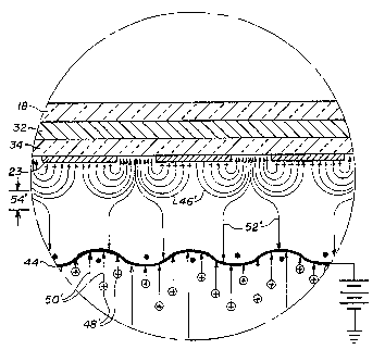
During development, negatively-charged matrix
particles 48, shown in FIG. 5, are expelled into the
volume adjacent to the grid-developing electrode 44. The
resulting body of space charge creates a substantially
uniform, normal electric space charge field component 50
outside the grid-developing electrode 44. This
space-charge field component 50 is directed away from the
photoconductive layer 34 and acts to propel the
negatively-charged matrix particles 48 through the
opposing drag forces of the ambient air toward the
photoconductive layer 34. The magnitude of the
space-charge field may range from a few tenths of a kV/cm
to several kV/cm; it is governed by the geometry of the
developer 42 and the physical properties of the
negatively-charged matrix particles 48. In particular,
the space-charge field strength is proportional to the
flow rate with which the negatively-charged matrix
particles 48 leave the developer 42,and it is substantially ,
independent of any potentials in the approximate range of
zero to °2000 volts that might be applied to the
grid-developing electrode 44. The purpose of the
grid-developing electrode 44 is to establish a spatially
uniform equipotential surface, controlled by an externally
applied potential or bias voltage, near the
photoconductive layer 34. By this means, the space-charge
field lines 50 are terminated, and a separate,
substantially uniform normal field component 52, in the
volume between the photoconductive layer 34 and the
grid-developing electrode 44, becomes proportional to the
difference between the potential applied to the electrode
44 and the spatial average of the positive potential from
the latent image on the layer 34, and becomes inversely
proportional to the distance from the layer 39 to the
electrode 94.
~~3'~
VVO 91/06114 P4.','T/US90/05307
- 9 -
This uniform field component 52 adds vectorially to the
existing latent image field near the surface of the
photoconductive layer 34, as shown in FIG. 5, producing a
negligible degree of distortion to the field lines 46 of
the latent image field. This negligible distortion does
not, however, intensify the latent image field nnr
straighten the field lines 46 associated with the image
field. The resultant electric field undergoes a
transition in a narrow zone 54 located at a distance from
the photoconductive layer 34 approximately equal to
three-fourths of the repeat period of the latent image
pattern (typically less than lmm). The grid-developing
electrode 44 must be positioned beyond this distance, for
the proper operation of the developing process. At
distances greater than the distance to the transition zone
54, the electrical force on the approaching
negatively-charged matrix particles is dominated by the
substantially uniform field component 52 controlled by the
grid-developing electrode 44. At lesser distances, i.e.,
between the photoconductive layer 34 and the transition
zone 54, the rapidly strengthening latent image field
becomes dominant.
In the aboveicited U.S. Pat. No. 4,921,767,
in Which no grid-developing electrode
is used, the substantially uniform space-charge field from
the body of negatively-charged matrix particles extends
directly to the latent image field near the surface of the
photoconductive layer 34. Fluctuations in the flow rate
with which matrix material is expelled from the developer
42 produce correlated fluctuations in the magnitude of the
space-charge field. When the space charge field is too
strong, it may reverse the direction of the repelling
component of 'the latent image field, in the unexposed
region at the surface of the photoconductive layer 34, and
thereby cause the particles to land at undesired, i.e.,
unexposed,locations on the photoconductive layer. A
somewhat weaker space charge field does not reverse the
repelling component of the latent image field, but may
~~~'~3~
W~ 91/06114 PCT/IJS90/05307 _.,.
-10-
shift the location of the field transition zone too close
to the photoconductive layer 34. When such a shaft
occurs, negatively-charged matrix particles with high mass
density, high triboelectric charge and/or large size, may
acquire enough momentum toward the photoconductive layer
34 to traverse the narrow space of repelling forces and
thereby land at the above-described undesired_locations.
In the present invention, the grid-developing electrode 44
is located at a distance substantially beyond that of the
transition zone 54, to provide a controlled,
substantially uniform electric field component 52 beyond
the range of the latent image field. Such a location for
the grid°developing electrode 44 shields the latent image
field, represented by field lines 46, from the effects-of
the space charge field 50 created by the space charge of
the particles expelled by the developer 42. The bias
voltage on the grid-developing electrode 44 may be
adjusted. by taking into consideration the desired flow
rate of material from the developer 42 and the physical
properties of the negatively-charged matrix particles,
to minimize the deposition of matrix particles on
the undesired locations of the photoconductor. The
potential applied to the grid-developing electrode .44
should be mare negativ~'than the spatial average of the
potential from the latent image,in order that the
substantially uniform field component 52, outside the
transition zone 54, acts to attract the negatively-charged
matrix particles 48 to the photoconductive layer 34.
Useful values for the potential on the grid electrode 44
range from zero to about °2000 volts. If the uniform
electric field component 52, established by the
grid-developing electrode 44, is weaker than the electric
field 50 from the body of space charge, the grid field
cannot support a material flow rate as high as the rate at
which negatively°charged matrix particles are expelled
from the developer 42. Consequently, the grid-developing
electrode 44 will collect a fraction of the '
negatively-charged matrix particles, while the remaining
WO 91!06114 Z p ~ ~ ~ ~f ~d PCT/US90l05307
-11 -
fraction will continue toward the photoconductive layer 34
at a lower flow rate commensurate with the reduced field
intensity between the grid-developing electrode 44 and the
photoconductive layer 34. Conversely, if the uniform
electric field component 52 between the grid-developing
electrode 44 and the photoconductive layer 34 is equal to
or stronger than the electric field 50 of the space
charge, few negatively-charged matrix particles 48 will be
collected by the grid-developing electrode 44. The
particles 48 will tend, instead, to pass through the
openings of the grid-developing electrode 44 and to be
accelerated to the new flow velocity associated with the
higher electric field component 52. Negatively-charged
matrix particles are propelled through the transition zone
54 and attracted to the positively-charged, unexposed
area of the photoconductive layer 34, to form the matrix
layer 23, by a process called direct development.
Infrared radiation may then be used, as shown in
FIG. 3e, to fix the particles 48 of matrix material by
melting or thermally bonding the polymer component of the
matrix material to the photoconductive layer,to form the
matrix 23.
The photoconductive layer 34 containing the matrix
23 is uniformly recharged to a positive potential of about
200 to 500 volts, for the application of the first of three
color-emissive, dry-powdered phosphor screen structure
materials. The shadow mask 25 is re-inserted into the
panel l2,and selective areas of the photoconductive layer
34, corresponding to the locations where green-emitting
phosphor material will be deposited, are exposed to
visible light from a first location within the lighthouse
40 to selectively discharge the exposed areas. The first
light location approximates the incidence angle of the
green phosphor-impinging electron beam. When there are no
other charged materials or conducting electrodes in
proximity to the photoconductive layer 34, the latent
image from the single exposure produces a latent image
CA 02067392 2000-12-21
_ 12 _
field represented by curving electric field lines 46', shown in FIG. 6,
that extend from the unexposed positively-charged regions to the
exposed discharged regions. The electric field lines 46' are
substantially parallel to the photoconductive layer 34 over the regions
where the surface charge varies most abruptly in position, and they are
substantially normal to the surface at those portions of the
photoconductive layer 34 where the latent image has little spatial
variation. When the lateral spacing between the light-exposed regions
where green-emitting phosphor material will be deposited is in the range
of 0.30 to 0.90 mm, typically 0.76 mm, and the initial surface potential
is in the preferred range of +200 to +700 volts, the peak magnitude of
the latent image field at the photoconductive layer 34 is in the range of
tens of kV/cm. Unlike the three superimposed light exposures from
three lamp positions previously used for the black matrix pattern, the
light exposure from a single lamp position produces exposed regions that
are typically several times narrower than the unexposed regions; as a
result, the normal field components at the surface are substantially
stronger in the narrow exposed regions than in the wider unexposed
regions. The magnitude of the electric field near the surface of the
photoconductive layer 34 diminishes rapidly with distance away from the
surface, and it is reduced to a peak value of a few tenths of a kV/cm at
a separation equivalent to about 3/4 the period of the latent image
pattern for the green-emitting phosphor locations.
After the exposure of the locations where the green-emitting
phosphor will be deposited, the shadow mask 25 is removed from the
panel 12 and the panel is moved to a second developer 42 having a grid-
developing electrode 44 and containing suitably prepared dry-powdered
particles of green-emitting phosphor. The phosphor particles are
surface-treated with a suitable charge controlling material, as described
in U.S. Pat. No. 4,921,727, issued to P. Datta et al. on May 1, 1990,
and U.S. Pat. No. 5,012,155, issued April 30, 1991 to Datta et al.
~C~~l~
WO 91/06114 PCT/U~90/05307
m 3_
The positively-charged green-emitting phosphor
particles are expelled from the developer, repelled by the
positively-charged areas of the photoconductive layer 34
and matrix 23, and deposited onto the discharged,
light-exposed areas of the photoconductive layer 34,in a
process known as reversal developing. As shown in F'IG. 7,
the expulsion of a substantial quantity of
positively-charged-green-emitting phosphor particles 48'
into the volume adjacent to the grid-developing electrode
44 creates a separate, nearly uniform, normal electric
space charge field component 50' outside the
grid-developing electrode 44. This space-charge field
component 50' is directed toward the photoconductive layer
34 and acts to propel the positively charged,
green-emitting phosphor particles 48' through the opposing
drag forces of the ambient air to the vicinity of the
photoconductive layer 34. The magnitude of the
space-charge field may range from a few tenths of a kV/cm
to several kV/cm, and is governed by the geometry of the
developer and the physical properties of the
positively-charged, green-emitting phosphor particles. In
particular, the space-charge field strength is
proportional to the flow rate with which the
positively-charged, green-emitting phosphor particles 48'
leave the developer 42, and it is substantially independent
of potentials in the approximate range of zero to +2000
volts that might be applied to the grid-developing
electrode 44. The grid-developing electrode 44 is
positively biased to a voltage in the range of +200 to
+1600 volts, depending on the spacing between the
electrode 44 and the photoconductive layer 34. The closer
the spacing, the lower the voltage required to establish
~~~~~~r~
1~0 91/06114 ~ ~ PC'f/U590/OS307-
-14-
the desired substantially uniform electric field 52'
between the electrode,44 and the photoconductor layer 34.
The strength of this field 52' establishes the desired
velocity of the phosphor particles as they approach the
previously described electric field transition zone 54',
which lies typically less than about lmm from the surface
of the photoconductor layer 34. In the absence of a
grid-developing electrode, the propelling effect of the
space-charge field from the body of positively-charged
phosphor particles expelled by the developer 42 may be
strong enough to substantially reduce the repelling effect
of the latent image field in the exposed region of the ,
photoconductive layer 34. The resultant normal component
of the latent image field near the surface of the
photoconductive layer 34 may not be effective to repel the
positively-charged, green-emitting phosphor particles, in
reversal development, from the areas of the photoconductive
layer that should be free of green phosphor. Accordingly,
cross-contamination occurs,unless the grid-developing
electrode 44 is utilized during phosphor development.
The positive potential applied to the grid-
developing electrode 44 is adjusted according to the
desired flow rate of phosphor material from the developer
_,. ..
42, and according to such physical properties as size,
mass density, and charge of the green-emitting phosphor
particles, in order to minimize the deposition of
particles in undesired locations. The potential applied
to the grid-developing electrode 44 should be more
positive than the spatial average of the potential from
the latent image, in order that the substantially uniform
field 52' outside the transition zone 54' attractsthe
positively-charged phosphor particles 48' to the
phetoconductive layer 34. If the field 52' established by
the grid-developing electrode 44 is weaker than the field
50' from the body of space charge, the grid field cannot
support a material flow rate as high as the rate at which
phosphor particles 48' are expelled by the developer 42.
Consequently, the grid-developing electrode 44 will
WO 91/06114 ~ ~ ~ '~ ~ ~ ;~ PGT/U~90/05307
-1S-
collect a fraction of the positively-charged phosphor
particles, while the remaining fraction continues toward
the photoconductive layer 34 at a lower flow rate
commensurate with the reduced field intensity between the
grid-developing electrode 44 and the photoconductive layer
34. Conversely, if the field 52' between the
grid-developing electrode 44 and the photoconductive layer
34 is equal to or stronger than the field 50' of the space
charge, few positively-charged phosphor particles will be
collected by the grid-developing electrode 44. The
particles 48' will, instead, pass through the openings of
the grid-developing electrode 44 and be accelerated to the
new flow velocity associated with the higher field 52'.
The phosphor particles 48' are thus propelled through
the transition zone 54' and attracted to the discharged,
exposed areasof the photoconductive layer 34. The
deposited green-emitting phosphor particles are fixed to
the photoconductive layer as described below
The photoconductive layer 34, matrix 23 and green
phosphor layer (not shown) are uniformly recharged to a
positive potential of about 200 to 700 volts,for the
application of the blue-emitting phosphor particles of
screen structure material. The shadow mask is reinserted
into the panel l2,and selective areas of the
photoconductive layer 34 are exposed to visible light from
a second position within the lighthouse 40, which
approximates the incidence angle of the blue
phosphor-impinging electron beam, to selectively discharge
the exposed areas. The shadow mask 25 is removed from the
panel l2,and the panel is moved to a third developer 42
containing suitably prepared dry-powdered particles of
blue-emitting phosphor. The phosphor particles are
surface-treated, as described above, with a suitable
charge controlling material, to provide a positive charge
on the phosphor particles. The dry-powdered,
triboelectrically-positively-charged, blue-emitting,
phosphor particles are expelled from the third developer
WO 91!05114 ~ ~ ~ '~ ~ J~ ~ PCT/US90l09307.-_
-l6-
42, propelled to the transition zone 54' by the
controlled, substantially uniform field 52' of the biased
grid-developing electrode 44; repelled from the
positively-charged areas of the ptiotoconductive layer 34,
the matrix 23 and the green phosphor material; and
deposited onto the discharged, light--exposed areas of the
photoconductive layer. The deposited blue-emitting
phosphor particles may be fixed to the photoconductive
layer, as described below.
The processes of charging, exposing, developing arid
fixing are repeated again for the dry-powdered,
red-emitting, surface-treated phosphor particles. The
exposure to visible light, to selectively discharge the
positively-charged areas of the photoconductive layer 34,
is from a third position within the lighthouse 40, which
approximates the incidence angle of the red
phosphor--impinging electron beam. The dry-powdered,
triboelectrically-positively-charged, red-emitting
phosphor particles are expelled from a fourth developer
42, propelled to the transition zone 54' by the
controlled, substantially uniform field 52' of the
grid-developing electrode 44; repelled from the
positively-charged areap of the previously deposited
screen structure materials; and deposited onto the
discharged areas of the photoconductive layer 34.
The phosphors may be fixed by exposing each
successive deposition of phosphor material to infrared
radiation, which melts or thermally bonds the polymer
component to the photoconductive layer 34. Subsequent to
the fixing of the red-emitting phosphor material, the
screen structure material is filmed and then aluminized,
as is known in the art.
The faceplate panel 12 is baked in air,at a
temperature of 425oC for about 30 minutes,to drive off
the volatilizable constituents of the screen,including the
conductive layer 32, the photoconductive layer 34 and the
solvents present in bath the screen structure materials
WO 91!06114 ~, ~ ~ ~7 ~ ~ ;~ PCT/US90/05307
-1'7-
and in the filming material. The resultant screen
assembly may possess higher resolution (as small as O.lmm
line width obtained using a resolution target), higher
light output than a conventional wet processed screen, and
greater color purity because of the reduced
cross-contamination of the phosphor materials.
In prior applications of electrophotography to
office copying machines (see, e.g.,U.S. Pat. No. 2,789,109,
issued to Walkup on Mar. 5, 1957), a developing electrode
is used. The use is to eliminate the edge-enhancement effects
encountered in the development of uniformly charged, i.e.,
unexposed or partially exposed, areas that are
substantially larger than the width of the line strokes in
typical printed lettering.which~are typically of the order
of 0.5 to l.0mm. In these applications, the electrode is
spaced substantially closer to the photoreceptive layer
than the diameter of the area to be uniformly developed,
i.e., the unexposed areas, and the applied potential is
large enough to significantly straighten the curving
electric field lines near the edges of the charged image
areas. Such an electrode ~;s not required for developing
small dark areas such as lines, letters, characters and
the like, which have a size comparable to the smallest
dimension of the phosphor and matrix lines of a CRT screen.
In contrast to this usage,the grid-developing electrode 44
used for electrophotographically manufacturing the screen
assembly of a color CRT in the present invention is
structurally and functionally different from the electrode
used in a copy machine. The novel grid electrode 49 is
placed at a distance (typically 0.5 to 4.0cm) from the
photoconductive layer 34 that is relatively large compared
to, e.g.,equal to or greater than six times, the characteristic
size of the smallest dimension of the unexposed latent image
areas (approximately 0.75mm for phosphor, and 0.25mm for~matrixD
WO 91/0611$ ~, ,, F~ ~l PCT/U590/05307,-.
.;
2 ~ ~ ~ ~.. '~ :~
-.18-
and lies outside the effective range of the spatially
varying latent image field (46 and.46~). Furthermore, the
magnitude of the potential applied to the grid electrode
44 is purposely restricted to a range of values which
produce little distortion of the highly localized latent '
image field,so that intensification and straightening of
the field lines does not occur.
The novel grid-developing electrode 44 provides a
more uniform deposition of phosphor, without
cross-contamination, than is possible in dry-powder
processes without such an electrode. The electrode also
provides means for tailoring the amount of phosphor
deposited on different areas of the faceplate, analogous
to the conventional slurry screening process where screen
weight variations are achieved by controlling slurry
thickness and the light intensity distribution of the
lighthouse. In the present process, screen weight is
controlled by the bias potential applied to the
grid-developing electrode 44 and the distance between the
electrode 44 and the photoconductive layer 34 on the
faceplate 18. The grid-developing electrode is generally
contoured to conform to the curvature of the faceplate;
however, it can be tailored to compensate for
_,. ,
non-uniformities in the phosphor developing apparatus or
to achieve a desired non-uniformity in phosphor screen
weight. Additionally, the apparatus and process described
herein may b,e utilized to screen a variety of tube sizes
on the same developer with only a change in the size of
the grid-developing electrode.