Note : Les descriptions sont présentées dans la langue officielle dans laquelle elles ont été soumises.
2~675~2
FREQUENCY DOUBLER WITH A VARIABLE DELAY CIRCUIT
AND EXCLUSIVE OR GATE
BACKGROUND OF THE INVENTION
The present invention relates to a doubling circuit
for doubling the frequency of an input signal and, more
particularly, to a doubling circuit for adjusting the duty
ratio of an output signal thereof automatically and
implemented as a digital circuit.
A conventional doubling circuit for the above
application has an input matching circuit to which an input
signal is applied, a non-linear circuit implemented by a
transistor, and an output matching circuit to which a load is
connected. The input matching circuit matches the input
signal to the input portion of the non-linear circuit while
the output matching circuit 14 matches a signal whose
frequency is double the frequency of the input signal to the
output portion of the non-linear circuit. In operation, the
input signal is routed through the input matching circuit to
the non-linear circuit to be distorted thereby. As a result,
high frequencies which are integral multiples of the frequency
of the input signal appear at the output portion of the non-
linear circuit. As the output signal of the non-linear
circuit is applied to the output matching circuit, the
matching circuit selects only the frequency double the
frequency of the input signal from the input signal. The
resulting output signal of the matching circuit, i.e., a
70815-119
2067562
signal whose frequency is double the frequency of the input
signal is fed to the load.
As stated above, it has been customary to match the
frequency at stages just before and just after the non-linear
circuit. This makes it difficult to adjust the duty ratio of
the output signal to, for example, 50 percent and, therefore,
requires troublesome adjustment every time the circuit is
reproduced. Although the non-linear circuit may be
implemented by a coil or similar analog element, an analog
element is apt to introduce errors in the circuitry due to the
scattering among such elements and, moreover, obstructs the
LSI configuration of the circuit. In addition, the
conventional doubling circuit is not applicable to a digital
configuration unless a signal having a sinusoidal waveform is
transformed to a signal having a rectangular waveform.
SUMMARY OF THE INVENTION
It is therefore an object of the present invention
to provide a doubling circuit which adjusts the duty ratio of
an output signal thereof automatically and can be implemented
as a digital circuit.
According to a first broad aspect, the invention
provides a doubling circuit for doubling a frequency of an
input signal, comprising: variable delay means for delaying
the input signal to produce a delayed signal; exclusive-OR
(EOR) gate means for EORing the delayed signal from said
variable delay means and the input signal to produce an EOR
signal; low pass filter (LPF) means for filtering the EOR
70815-119
2~67562
signal from said EOR gate means to produce a filtered signal;
and integrating circuit means for integrating a voltage
difference between the filtered signal from said LPF means and
a reference voltage to produce an integrated signal; said
variable delay means delaying the input signal a period of
time controlled by the integrated signal from said integrating
circuit means and said EOR signal having double the frequency
of the input signal.
According to a second broad aspect, the invention
provides a method of doubling a frequency of an input signal,
comprising the steps of: (a) delaying the input signal a
predetermined period of time to produce a delayed signal; (b)
EORing the input signal and the delayed signal to produce an
EOR signal, which has double the frequency of the input
signal; (c) low-pass filtering the EOR signal to produce a
filtered signal; and (d) integrating a voltage difference
between the filtered signal and a reference signal, whereby
the period of time by which the input signal is to be delayed
is controlled.
BRIEF DESCRIPTION OF THE DRAWINGS
The above and other objects, features and advantages
of the present invention will become more apparent from the
following detailed description taken with the accompanying
drawings in which:
,~
70815-119
2067562
FIG. 1 is a block diagram schematically showing a
conventional doubling circuiti
FIG. 2 is a block diagram schematically showing a
doubling circuit embodying the present invention; and
5FIG. 3 is a timing chart representative of a specific
operation of the embodiment.
20~7~6~
DESCRIPTION OF THE PREFERRED EMBODIMENT
To better understand the present invention, a brief
reference will be made to a con~entional doubling circuit, shown
in FIG. 1. As shown, the doubling circuit, generally 10, is
5 made up of an input matching circuit 12 to which an input signal
11 is applied, a non-linear circuit 13 implemented by a
transistor 13 a, and an output matching circuit 14 to which a
load 15 is connected. The input matching circuit 12 matches the
input signal 11 to the input portion of the non-linear circuit 13.
10 The output matching circuit 14 matches a signal whose frequency
is double the fre~uency of the input signal 11 to the output
portion of the non-linear circuit 13.
In operation, the input signal 11 is routed through the
input matching circuit 12 to the non-linear circuit 13 and
15 distorted by the circuit 13. As a result, high frequencies which
are integral multiples of the frequency of the input signal 11
appear at the output portion of the non-linear circuit 13. As the
output signal of the non-linear circuit 13 is applied to the output
matching circuit 14, the matching circuit 14 selects only the
2 0 frequency double the frequency of the input signal 11 from the
input signal. The resulting output signal of the matching circuit
14, i. e., a siænal whose frequency is double the frequency of
the input signal 11 is fed to the load 15.
As stated above, the conventional doubling circuit 10
2 5 matches the frequency at stages iust before and just after the
6 2~67~62
non-linear circuit 13. This makes it difficult to adjust the duty
ratio of the output signal to, for example, 5 0 percent and,
therefore, results in the need for troublesome adiustment every
time the circuit is reproduced, as discussed earlier. While the
5 non-linear circuit 13 may be implemented by a coil or similar
analog element, an analog element is apt to introduce errors in
the circuitry due to the scattering among such elements and,
moreover, obstructs the LSI configuration of the circuit 10. In
addition, the doubling circuit 10 is not applicable to digital
10 circuitry unless a signal having a sinusoidal waveform is
transformed to a signal having a rectangular waveform.
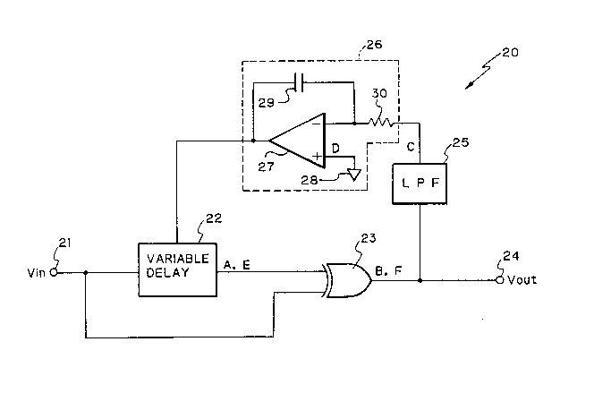
Referring to FIG. 2, a doubling circuit embodying the
present invention is shown and generally designated by the
reference numeral 20. As shown, the doubling circuit 20 has an
15 input terminal 21 to which an input signal Vin having a
rectangular waveform is applied. A variable delay circuit 2 2
delays the input signal Vin a controllable period of time, which
will be described, to produce an output signal A or E. An
exclusive-OR (EOR) gate 23 EORs the output signal A or E of the
variable delay circuit 22 and the input signal Vin fed from the
input terminal 21. The output sig~al, i. e., EOR signal B or F
of the EOR gate 23 is fed out via an output terminal 24 as an
output signal Vout while being delivered to a low-pass filter
(LPF) 25. The LPF 25 produces a mean voltage C of the signal
B or F by filtering the signal B or F. An integrating circuit 26
~7~ 2~7~62
has an operational amplifier (OP AMP) 27, a reference voltage
terminal 28, a capacitor 29, and a resistor 30. The output
voltage C of the LPF 25 is applied to the inverting input of the OP
AMP 27 via the resistor 30 while a reference voltage D is applied
5 to the non-inverting input of the OP AMP 27 via the reference
voltage terminal 28. The OP AMP 27 integrates a difference
between the input voltagés C and D. The resulting output of the
OP AMP 27 is delivered to the variable delay circuit 22 and is fed
back to the inverting input of the OP AMP 27 via the capacitor
10 29. The delay of the variable delay circuit 22 is controlled by
the output of the integrating circuit 26.
The operation of the doubling circuit 20 will be described
with reference also made to FIG. 3. To begin with, assume that
the delay of the variable delay circuit 22 is controlled to
15 one-eighth of the period of the input signal Vin by way of
example. Then, the variable delay circuit 22 outputs the signal
A. The EOR gate 23 produces EOR of the input signal Vin and
the delayed signal A, i. e., the signal ~ whose frequency is
double the frequency of the input signal Vin. Since the delay of
20 the variable delay circuit 22 is one-eighth of the period of the
input signal, the EOR signal B has a duty ratio of about 25
percent. The LPF 25 filters the si~nal B having a duty ratio of
25 percent to thereby output a mean voltage C of 1. 25 volts.
The mean voltage C is proportional to the duty ratio of the
25 signal B, e. g., the former is 2. 5 volts if the latter is 50 percent
-8- 2~6 7~ 62
or 5 volts if the latter is 100 percent.
To give the output signal B of the EOR gate 2 3 a duty
ratio of, for example, 5 0 percent, the reference voltage D
applied to the integrating circuit 26 is adiusted to 2. 5 volts. As
the output of the integrating circuit 26 is fed back to the variable
delay circuit 22, the delay of the delay circuit 22 is controlled to
one-fourth of the period of the input signal Vin. As a result,
the variable delay circuit 22 produces the other signal E. Then,
the EOR gate 23 produces EO~ of the input signal Vin and the
signal E, i. e., the signal F having a duty ratio of about 50
percent. By such a procedure, the input signal ~in is doubled in
fre~ uency to output a signal whose duty ratio is about 5 0
percent.
As stated above, only if the reference voltage D to be
applied to the integrating circuit 2 6 is adequately selected, the
embodiment adiusts the duty ratio of the doubled signal
automatically in response to the output of the integrating circuit
26, i. e., the result of integration of the difference between the
output voltaæe of the LPF 25 and the reference voltage D. This
eliminates the need for the conventional complicated adjustment.
Further, since the doubling circuit 20 is entirely implemented as
a digital circuit including no analog elements, it is free from
errors ascribable to the scattering among elements and can be
readily incorporated in an LSI configuration.
2 5 In summary, it will be seen that the present invention
2~756~
_g_
provides a doubling circuit which adjusts the duty ratio of a
doubled signal automatically and, therefore, does not need any
complicated adjustment when reproduced. This unprecedented
advantage is derived from the unique construction wherein a low
5 pass filter filters a doubled signal, an integrating circuit
integrates a difference between the output voltage of the low
pass filter and a reference voltage, and a variable delay circuit
has the delay thereof controlled by the output of the integrating
circuit. Another adYantage achievable with the invention is that
10 since the doubling circuit is implemented as a digital circuit
including no analog elements, it eliminates errors ascribable to
the scattering among elements and can be incorporated in an LSI
configuration with ease.
Various modifications will become possible for those
15 skilled in the art after receiving the teachings of the present
disclosure without departing from the scope thereof.