Note : Les descriptions sont présentées dans la langue officielle dans laquelle elles ont été soumises.
2068815
I
AN OPTICAL SWITCHING SYSTEM
Tecunical Field
This invention relates to the switching of data and, in particular, to the
optical switching of data.
5 Back~round of the Invention
Prior art optical switching systems that utilize time division multiplexing
require electrical interfaces at the inputs and outputs of an optical switch. The input
interfaces receive optical data from optical links, convert the optical data to electrical
data, buffer and synchronize the electrical data, and convert the electrical data to
10 optical data for switching by the optical switch. The output interfaces perform the
same function but in the reverse order. One such prior art optical switching system
is set forth in the article entitled "Broadband Photonic Switching Using Guided-Wave Fabrics", IEEE LTS Journal, N.K. Ailawadi et al., May 1991, Vol. 2, No. 2,
pp. 36-43.
The electrical buffering and synchronizing on the inputs and outputs of
the optical switch ensures that data is transmitted and received in the correct time
slots in relation to the timing of the optical switching system. The need for such
interfaces is unfortunate since present optical switching technology allows for nearly
unlimited bandwidth on optical communication paths through an optical switch.
20 However, these paths are relatively expensive, making time division multiplexing
highly desirable so that multiple channels can share a common path. Further, theneed for electronic buffering detracts from the advantages of an optical switch
because generally data which can be electronically buffered, stored and synchronized
to accomplish the time division multiplexing within the switching system can also be
25 electronically switched within an electronic switching system at the same rate as the
buffering.
Summary of the Invention
In accordance with one aspect of the invention there is provided an
optical system having all optical communication paths for communication of data,30 comprising: a plurality of terminals; a plurality of optical links; an optical switching
unit for providing all optical communication paths between one of said plurality of
terminals and another one of said plurality of terminals via said optical links; means
2068815
- la-
physically located with said optical switching unit and interconnected to said
plurality of optical links responsive to information transmitted via said optical links
from said plurality of terminals for synchronizing the internal timing of said plurality
of terminals with that of said optical switching unit; and said synchronizing means
comprises means for blocking data information from one of said plurality of
terminals not in synchronization with said optical switching unit from being switched
by said optical switching unit.
In accordance with another aspect of the invention there is provided an
optical switching unit for interconnecting terminals via a plurality of input optical
links and a plurality of output optical links, comprising: a plurality of optical input
interfaces each connected to one of said plurality of input optical links and; aplurality of optical output interfaces each connected to one of said plurality of output
optical links; an optical network for interconnecting one of said plurality of optical
input interfaces and one of said plurality of optical output interfaces to create an al
optical communication path through said one of said plurality of optical input
interfaces and said one of said plurality of optical output interfaces and said optical
network; means physically located with said optical network and interconnected to
said plurality of optical links responsive to information received from each of said
terminals for synchronizing the timing of each of said terminals with that of said
optical switching unit via said plurality of output optical links said synchronizing
means comprises means for determining the timing of said terminals via said
plurality of input optical links; and means responsive to determination of incorrect
timing for adjusting the timing of said terminals via said plurality of output optical
links.
In accordance with yet another aspect of the invention there is provided
a method for controlling an optical system having all optical communication paths
for communication of data and said optical system having a plurality of terminals, a
plurality of optical links, an optical switching unit and a synchronizing unit physical
located with said optical switching unit and interconnected to said plurality of optical
links, said method comprising the steps of: providing all optical communication
paths through said optical switching unit between one of said plurality of terminals
and another one of said plurality of terminals via said optical links; synchronizing
2068815
- Ib-
the internal timing of said plurality of terminals with that of said optical switching
unit in response to information transmitted via said optical links from said plurality
of terrninals; and blocking data inforrnation from one of said plurality of terminals
not in synchronization with said optical switching unit from being switched by said
5 optical switching unit.
206881~
In an illustrative embof3iment, the optical switching unit comprises an
optical network, system clock, optical input interfaces for receiving h~follnation
from the terminals, and optical output interfaces for tran~mitting info.~nation to the
terminals. The system clock determines the timing of each terminal using
5 information transmitted to an individual optical input interface by each terminal~ If
the timing of a terminal does not match that of the system clock, the system clock
blocks the transfer of data information by the optical input interface to the optical
network and transmits corrective timing inform~tion to the termin~l via an optical
output interface. If the timing matches, the system clock signals the optical input
10 interface to com~ icate the data information to the optical network which switches
the data information to optical output interfaces for tr~nsmi~sion to termin~ls.Timing information and data information are col.. ,.. -icafe~l with
terminals using different optical wavelengths. An optical input interface separates
these two optical wavelengths for use by the optical switching unit; whereas, an15 optical output interface combines these wavelengths for tr~n~mi~siQn to a terminal.
Other and further aspects of the present invention will become apparent
during the course of the following description and by reference to the accompanying
drawing.
Brief Description of the D. aWil-~
FIG. 1 illustrates, in block diagram form, an optical switching unit with
attached terminals embodying the inventive concept;
FM. 2 illustrates the manner in which data and timing information is
communicated between the optical switching unit and the terminals;
FIG. 3 illustrates, in block diagram form, the clock system of the optical
25 switching unit;
FIG. 4 illustrates, in block diagram form, a termin~l embodying the
inventive concept; and
FIG. S illustrates, in block diagram form, a wavelength division
demultiplexer of the optical switching unit.
30 Detailed Description
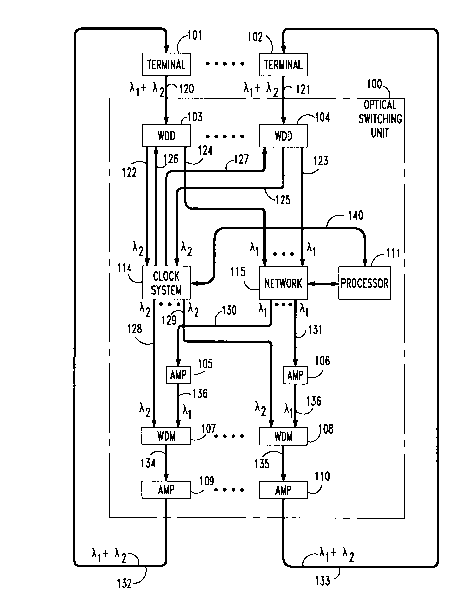
FIG. 1 iIlustrates terminals 101 through 102 connected to optical
switching unit 100 via input optical links 120 through 121 and output optical
links 132 through 133, respectively. In accordance with the invention, tr~nsmi~sion
of data signals from one terminal to other terminals through optical switching
35 unit 100 is done entirely by optical devices, and the data signals are never converted
to electrical signals. Optical links 120 through 121 and 131 through 133 are capable
2068815
- 3 -
of carrying two optical wavelengths, each being a separate logical path. Opticalswitching unit 100 optically comlll.lllicates data information among terminals 101
through 102 using time division multiplexing techniques. For example, terminal 101
tr~n~mit~ optical signals using wavelengths ~1 and ~2 on optical link 120 and
5 receives optical signals over path 132 using the same wavelengths. Wavelength ~ 1
is used to designate the data optical wavelength used for tr~nsmicsion of data signals,
and ~2 is used to designate the timing optical wavelength used for tr~n~mi~sion of
timing control information within the optical switching system.
The two optical wavelengths tr~nsmitted from terminal 101 via optical
10 link 120 are received by wavelength division demultiplexer (WDD) 103 which is an
optical input interface. Wavelength division ~lem~lltiplexer 103 separates the two
optical wavelengths and applies data optical wavelength ~ l to optical switch
network 115. The timing optical wavelength ~2 is applied to the clock system 114via optical path 122. Clock system 114 uses information communicated via timing
15 optical wavelength ~2 to determine if terminal 101 is in frame synchronization with
clock system 114. If terminal 101 is in frame synchronization, clock system 114
enables wavelength division demultiplexer 103 to co--""~ icate the data optical
wavelength ~ 1 from input optical link 120 to network 115. If terminal 101 is not in
frame synchronization, clock system blocks the communications of data optical
20 wavelength ~ 1 through wavelength division demultiplexer 103 and transmits control
information via wavelength division multiplexers (WDMs) blocks 107 and 108 and
output optical link 132 to terminal 101 to frame synchronize terminal 101. Framesynchronization is described in greater detail with respect to FIG. 2.
Each termin~l receives and transmits a frame of time slots. The terminal
25 extracts data from time slots assigned to the terminal by processor 111 and transmits
data in time slots of the frame also assigned to the terminal using well known
techniques. Network 115 is of the time division multiplexing type which is well
known to those skilled in the art, opel ~ting under control of processor 111 in a
conventional manner, takes data in particular time slots from particular terminals and
30 switches that data into time slots assigned to terminals designated to receive the data.
Time slot assignment information is tr~n~mitte~l to the terminals by processor 111
via bus 140 and clock system 114 in the timing optical wavelength ~2.
Network 115 may be advantageously fabricated using lithium niobate
devices. Alternatively, other optical switching devices may be used to fabricate35 network 115 including self electro-optic effect devices (collllllonly known as
"SEED" devices), ferroelectric liquid crystal devices, magneto-optical devices,
~068815
moving fiber type switches, or any other optical switching technology.
Advantageously, the switching network could also be a passive combiner with the
switching being effected by m~king each termin~l respond to one or more time slots.
Terminal 102 transmits optical wavelengths, ~ 1 and ~2 via optical
5 path 121 to wavelength demultiplexer 104. Wavelength division demultiplexer 104
separates the two optical wavelengths ~ 1 and ~2 and applies data optical wavelength
to optical network 115 via optical path 123 and applies tirning wavelength optical
~2 to the clock system 114 via optical path 125. Wavelength division
demultiplexers 103 and 104 contain optical shutters for blocking all data optical
10 wavelength ~ 1 information from being applied to the network 115 when the frame
timing of a terminal is determined to be incorrect by clock system 114. As notedearlier, when clock system 114 finds a given timing optical wavelength ~2 input
from a wavelength division demultiplexer to be in frame synchronization with thesystem clock, clock system 114 allows the data optical wavelength ~ 1 to be applied
15 from that wavelength division demultiplexer over an optical path to network 115.
The tr~n~mi~sion of information to the terminals is described in this
paragraph. Clock system 114 applies an optical timing control signal via timing
optical wavelength ~2 over optical path 128 to wavelength division multiplexer 107.
The data from network 115 is colllll,unicated by the data optical wavelength ~ 1 via
optical path 130 to optical amplifier 105. This wavelength is amplified by optical
amplifier 105 and applied to optical path 136 where it is received by wavelengthdivision multiplexer 107. Wavelength division multiplexer 107 combines the two
optical wavelengths from paths 136 and 128 to form a composite optical signal
which is tr~n~mitted via path 134 to optical amplifier 109. Optical amplifier 109
amplifies both wavelengths and tr~n~mit~ the composite optical signal, designated by
~ 1 + ~2, via path 132 to the terminal 101. Wavelength division multiplexer 107 and
optical amplifier 109 form an optical output interface. Blocks 106, 108, and 110function in a similar manner.
To frame synchronize the terminals, clock system 114 receives frame
30 clock information from the terminals via timing optical wavelength ~2 and
determines if the frame timing of an incoming timing signal from a given terminal is
in phase within a predetermined range of the master clock within the clock
system 114. This determination also allows clock system 114 to colllpellsate fordelays along the optical paths, particularly links 120 through 121 and 132
35 through 133, which tend to be longer and more variable than intern~l optical paths of
optical switching unit 100. If the frame timing is in phase, clock system 114 allows
2068815
.,
- 5 -
the data (transported via the data optical wavelength ~ 1) to be applied imm~i~tely
to network 115 by the actuation of the optical shutter of the a~pro~,l;ate wavelength
division multiplexer and signals the terminal not to adjust its frame timing. If the
frame timing is not in phase, clock system 114 signals via the timing optical
5 wavelength ~2 that the terminal is to advance or delay frame timing. This sign~ling
allows the terminal to become frame synchronized with the master clock of the clock
system 114. In accordance with the invention, all frames and time slots applied to
network l lS are frame synchronized and do not require any electrical buffering,additional frame synchronization, or rate conversion. Advantageously, this allows
10 network 115 and the entire optical switching system to be transparent to data rates
over a wide range. The result is that each time slot assigned to an individual
terminal may carry the data at arbitrary rates and have either analog or digital format.
Allowing users of optical switching system to albiLl~ily change the data rates and
formats as tennin~l technology permits.
lS In order to understand the operation of clock system 114, consider
FIG. 2 which illustrates signals of frames that are tr~nsmitte~ and received by
terminal 101. On line 201 of FIG. 2, the rising edge of pulses 202 and 205
designates the start of frames at the output of t~rmin~l 101 on timing optical
wavelength ~2 of link 120. Time slot 0, designated as 203, appears immediately
20 after the pulse 202 and successive time slots are shown up to time slot 4, designated
as 204, which is followed by pulse 205 designating a start of a new frame.
Pulses 202 and 205 are generated by terminal 101 and indicate the internal timing of
the terminal 101. The time slotted data from terminal 101 (L~ sl~-;L~e~l via data
optical wavelength ~ 1 of link 120) is illustrated by line 207 of FIG. 2. This time
25 slotted data may be con~pulel data, video data, voice data, a f~csimile data, or any
kind of analog or digital data. In line 207, for example, time slot 1, designated
as 208, and time slot 3, designated as 209, are in active use by termin~l 101.
Line 210 of FIG. 2 shows the data signal co.ll"~ icated to terminal 101
via path 132 from network 115. Time slots are tr~nsmitte~1 and distinguished from
30 one another using techniques well known in the art. Time slot 1 is active and the
other times slots are inactive. Corresponding to line 210 is line 220 which illustrates
the timing control signals from the clock system 114 having pulses 214 and 215
which designates the start of frames and having digitally encoded phase error
information designated by bits 212 through 213 in time slot 0. In addition, bits 216
35 through 217 in time slot 1 contain information assigning time slots ~ ctermined by
processor 111. When pulses 214 and 215 are received by terminal 101, they are
206881S
-
- 6 -
distinguished from digitally encoded phase error bits 212 through 213 using
techniques well known in the art.
The details of clock system 114 are shown in FIG. 3. Master timing
source 311 of clock system 114 is advantageously a precision tuneable quartz crystal
S oscillator or phase locked loop that can lock its frequency to that of an incoming
signal of a precision digital facility (which is not illustrated) using well known
techniques. The frame timing control information from termin~l 101 is received by
the clock system 114 over optical path 122 via timing optical wavelength ~ 2 . This
information is converted from an optical signal to an electrical signal by optical
10 receiver 301 and applied via path 314 to phase comparator 302. Phase
comparator 302 compares the phase of the frame signal received from terminal 101with the phase of the frame signal received from master timing source 311 via
path 323. Phase comparator 302 produces an electrical signal which is an analog
signal proportional to the phase difference between the signals received via
15 paths 314 and 323 using techniques well known in the art. This analog signal is
applied via path 315 to low pass filter 312 where it is filtered and applied to error
signal encoder 303 via path 324.
Error signal encoder 303 converts the analog signal received via
path 324 into a digital representation. Error signal encoder 303 also generates an
20 optical shutter control signal that is tr~n~mitte~ via optical path 126 to wavelength
division demultiplexer 103 for the purposes of gating the data optical wavelength
from wavelength demultiplexer 103 to network 115 in the following manner. If theanalog signal received by error signal encoder 303 via path 324 is smaller than some
predefined value, this means that t~rmin~l 101 is frame synchronized and error signal
25 encoder 303 signals via path 126 to wavelength division demultiplexer 103 to allow
the data optical wavelength ~1 to be tr~nsmit~ecl to network 115 via path 124. On
the other hand, if the analog signal received by error signal encoder 303 via path 324
is larger than the predefined value, this means that termin~l 101 is out of frame
synchronization and error signal encoder 303 signals via path 126 to wavelength
30 division clçmllltiplexer 103 to block the data optical wavelength ~ 1 from
network 115.
If terminal 101 is out of frame synchronization, control information is
sent to terminal 101 as described in this paragraph. Error signal encoder 303
co.~ -nicates the digital representation of the analog signal it receives over
35 path 324 to protocol handler 304 via path 316. Protocol handler 304 formats this
digital representation from error signal encoder 303. In addition, protocol
21~6881S
handler 304 also formats the time slot assignment information received from
processor 111 via bus 140 and combines this infoln~ation with the information from
error signal encoder 303. The combined information is fo.l,.~ l for serial
tr~nsmi~sion over optical path 128 after it is converted from electrical to optical form
5 (timing optical wavelength ~2) by means of opdcal transmitter 305. Blocks 306
through 310 and 313 perform similar processing between optical input path 125 and
optical output path 130, and a similar assemblage of components would be
associated with each of the other terminals.
FM. 4 shows the details of termin~l 101. The combination of optical
10 wavelengths ~1 and ~2 iS applied to terminal 101 via path 132 from which they are
received by wavelength division demultiplexer 415. Here, the wavelengths ~1 and
;~2 are separated and transmitte~ on separate optical paths by demultiplexer 415.
The timing optical wavelength ~2 iS applied to optical receiver 425 via path 414.
Optical receiver 425 converts the timing optical wavelength ~2 to an electrical signal
15 which is applied to protocol termin~tc)r 413 via path 426. Protocol termin~tor 413
terminates the protocol which may advantageously be X.25, HDLC, or a similar bit-
oriented protocol and extracts the digitally encoded phase error signal and the time
slot assignment information. The latter il~fo~ ation is tr~nsmitted to data in
buffer 417 and data out buffer 421 via bus 426. The digitally encoded phase error
20 signal is applied via path 412 to clock control circuit 411. The latter circuit changes
the digitally encoded phase error signal to an analog voltage which controls voltage
tuneable oscillator 409.
The output of the oscillator is applied over path 408 to frame, time slot
and bit clock generator 405 in order to adjust the latter generator. Generator 405
25 produces three clock signals: frame clock, time slot clock, and bit clock.
Generator 405 applies the frame clock signals via path 404 to ~2 optical
tr~n~m;tter 403. Optical tr~n~mitter 403 receives the frame clock signal and converts
it into an optical signal on timing optical wavelength ~2 which is applied via
path 402 to wavelength division multiplexer 401. Additionally, the frame clock,
30 time slot clock, and bit clock signals are applied to data out buffer 421 over
paths 404, 406, and 407.
Now consider the data processing functions of terminal 101, as
illustrated in FIG. 4. Wavelength division ~çmultiplexer 415 applies the data signals
(commllnic~te~1 via data optical wavelength ~ l ) to data in buffer 417 via path 416,
35 optical receiver 427, and path 428. In response to time slot a~signment information
from protocol termin~tor 413, data in buffer 417 makes the data available to te~nin~l
2068815
functions 419 via path 418. Terrninal functions 419 performs the functions of
terminal 101. For example, if the terminal is an ordinary compu~er terminal attached
to a host, the received data would be displayed on the screen of the terminal, and the
output of the terminal functions 419 would be the output of the keyboard which is
5 sent back to the host. Terminal functions 419 applies its output via path 420 to data
out buffer 421. Data out buffer 421 uses the frame clock, time slot clock, and bit
clock signals to synchronize the output data for tr~n~mi~sion via path 422 and the
time slot assignment information from protocol terminator 413 to de~~ e
assigned time slots. If the output data is in analog form, only the frame and time slot
10 clocks are required. Optical tr~nsmitter 423 changes the electrical signal received
via path 422 into an optical data signal for comm~lnication by data optical
wavelength ~ 1. Data optical wavelength ~ 1 is transmitted via optical path 424 to
wavelength division multiplexer 401 where it is combined with the timing opticalwavelength ~2 which is received via path 402. Wavelength division multiplexer 401
15 combines the optical wavelengths into a composite optical signal ~ 1 + ~2 containing
both optical wavelengths ~ 1 and ~2. This composite optical signal ~ 1 + ~2 is
applied via optical link 120 to wavelength division demultiplexer 103 of FIG. 1.The details of wavelength division demultiplexer 103 are shown in
FIG. 5. Demultiplexer 501 receives an optical signal which is the composite optical
20 signal ~1 + ~2 over link 120. Demultiplexer 501 may advantageously be
implemented using focusing gratings or may be implemented using a number of
other optically dispersive techniques. All such techniques are well known in the art.
The separated timing optical wavelength ~2 is applied via path 122 to clock
system 114 of FIG. 1. The data optical wavelength ~ 1 is applied via path 502 to25 optical shutter 503. The purpose of the shutter is to prevent network 115 from
receiving non-synchronized data sent from terminals 101 before terminal 101 is
frame synchronized with the optical switching system. Advantageously, if
network 115 is a simple passive combiner, another purpose of the shutter 503 is to
prevent a terminal from destroying data in network 115 when the tennin~l is not
30 frame synchronized properly with respect to the frame and time slots of the other
terminals in the optical switching system. The shutter control signal is received via
path 126 from the clock system 114 as shown in FIG. 1. The shutter control signal
applied over path 126 may be electrical or optical depending on the shutter. Shutters
of this type are well known in the art.
21)~8815
g
Additionally, the circuitry disclosed herein is, of course, merely
illustrative. Indeed, although the various functional blocks disclosed herein are
depicted as discrete cilcuill;cs, those various functions could be carried out using
one or more programmed processors or digital signal processing (D~P) chips.