Note : Les descriptions sont présentées dans la langue officielle dans laquelle elles ont été soumises.
2068975
BACKGROUND OF THE INVENTION
[Field of the Invention]
This invention relates to an optical amplification
system suitably used for compensation of transmission loss
and improvement of signal reception sensitivity by using
an optical waveguide having a capability of optical
amplification by optical pumping.
[Prior Art]
Optical amplification systems using optical fibers
having an optical amplification capability have been known
and utilized as means for switching optical transmission
lines in optical CATV systems and other practical
applications.
There has been reported that light of 1.55~m band can
be effectively amplified by using a silicate glasss single
mode optical fiber having an erbium (Er)-doped core in an
optical amplification system of the above described type.
As illustrated in Fig. 9 of the accompanying
drawings, an optical amplification system under
consideration normally comprises a pumping source 31 for
optical pumping, an optical combiner 32 for combining
optical signals and pumped light and an optical fiber 33
having an rare earth element-doped core 33, to which an
1
2068975
optical isolator 34 is added.
A known optical amplification system as shown in Fig.
9 normally shows a rise of excitation level in the optical
fiber 33 when pumped light is introduced into the optical
fiber 33 and amplifies light signals fed to the optical
fiber 33 as it returns to a normal state from the raised
excitation level.
Such an optial optical amplification system has a
large gain and a high response speed and therefore is
capable of adapting itself to an ultra-high speed
transmission environment.
However, if no light signal is existent in the
optical fiber 33 for a considerable period of time, e.g.
several milliseconds, under a condition where pumped light
is constantly being introduced to the optical fiber 33,
the excitation level in the optical fiber 33 is raised
further so that the light signal introduced in the optical
fiber 33 under this condition is amplified by a large
amplification factor accordingly.
Thus, if the optical fiber 33 remains under a
condition where no optical signal is entered into it for a
long period of time and immediately thereafter an optical
signal is introduced there, the optical signal will be
amplified by a very large amplification factor to generate
intense optical pulses, which by turn can destruct and/or
2
2068975
saturate the downstream systems.
Figs. 10(A) and 10(B) of the accompanying drawings
illustrate waveforms obtained when a known optical
amplification system is used for a line switching system.
Of these illustrations, the waveform of Fig. 10(B),
which is obtained before it is optically amplified, shows
that the rising edge of the signal is amplified to
generate strong pulses as may be more clearly seen when
compared with that of Fig. 10(B) obtained after the
optical amplification.
In view of the above described problem of the prior
art, it is therefore an object of the present invention to
provide an optical amplification system that can operate
properly regardless of the waveform of the incoming
signal.
SUMMARY OF THE INVENTION
According to a first aspect of the present invention,
the above object is achieved by providing an optical
amplification system comprising an optical amplifier unit
having an optical waveguide capable of amplifying optical
signals transmitted through said optical waveguide by
means of the effect of optical amplification produced in
the optical waveguide when pumped light is fed to said
optical waveguide, wherein pumped light is fed to said
optical waveguide only when an optical signal is
3
2068975
transmitted through said optical waveguide whereas no
pumped light is fed to said optical waveguide as long as
no optical signal is transmitted through said optical
waveguide.
In an optical amplification system according to the
first aspect of the invention, auxiliary pumped light is
preferably fed to the optical waveguide on a constant
basis in order to enhance the responsiveness of the system
for optical amplification.
The optical amplifier unit of an optical
amplification system according to the first aspect of the
invention preferably comprises, besides the optical
waveguide for optical amplification, an optical combiner
for feeding the optical waveguide with pumped light, a
pumping source for generating pumped light and a drive
circuit for driving said pumping source. Alternatively,
the optical amplifier unit of an optical amplification
system according to the invention may comprise an optical
waveguide for optical amplification, an optical switch for
turning on and off the pumped light fed to the optical
waveguide, a pumping source for generating pumped light
and a drive circuit for driving said pumping source.
In order to enhance the responsiveness of the system
for optical amplification, a bias power source is
preferably connected to the pumping source of the optical
4
2068975
amplifier unit of an optical amplification system
according to the invention. Alternatively, it is
preferable that the optical amplifier unit comprises an
auxiliary pumping. source and a drive circuit for driving
the auxiliary pumping source. Still alternatively, it is
preferable that an auxiliary optical pumping unit is
arranged downstream to the optical amplifier unit in order
to fed auxiliary pumped light to the optical waveguide in
a direction reverse to that of transmission of optical
signals. The auxiliary optical pumping unit may be
replaced by an auxiliary optical amplifier unit of a
steadily operating type arranged upstream and connected to
the optical amplifier unit.
According to a second aspect of the present
invention, the above object is achieved by providing an
optical amplification system comprising an optical
amplifier unit having an optical waveguide capable of
amplifying optical signals transmitted through said
optical waveguide by means of the effect of optical
amplification produced in the optical waveguide when
pumped light is fed to said optical waveguide, wherein
pumped light is constantly fed to said optical waveguide
for steady excitation and a dummy optical signal is
applied to the optical waveguide whenever no optical
signal is transmitted through the optical waveguide
2068975
whereas no dummy optical signal is applied to the optical
waveguide as long as an optical signal is transmitted
through the optical waveguide.
The optical- amplif ier unit of an optical
amplification system according to the second aspect of the
invention comprises, besides the optical waveguide for
optical amplification, a pumping source for generating
pumped light and a drive circuit for driving said pumping
source and a dummy optical signal source is arranged
upstream and connected to the optical amplifier unit by
way of an optical switch.
with an optical amplification system according to the
first aspect of the invention, pumped light is fed to said
optical waveguide only when an optical signal is
transmitted through said optical waveguide whereas no
pumped light is fed to said optical waveguide as long as
no optical signal is transmitted through said optical
waveguide.
The pumped light fed to the optical waveguide goes
into the waveguide shortly after an optical signal is
transmitted into the optical waveguide. Therefore, no
optical amplification takes place in the optical waveguide
when there is a rising edge of an optical signal in the
optical waveguide and consequently the effect of optical
amplification of the unit is not affected by the waveform
6
2068975
of the optical signal being transmitted therethrough.
The optical waveguide will find itself in a highly
excited condition when properly pumped light is fed to the
optical waveguide of the above optical amplification
system while auxiliary pumped light is being fed there.
Consequently, the stability and the responsiveness of the
system will be so much more improved.
With an optical amplification system according to the
second aspect of the invention, pumped light is constantly
fed to said optical waveguide for steady excitation and a
dummy optical signal is applied to the optical waveguide
whenever no optical signal is transmitted through the
optical waveguide whereas no dummy optical signal is
applied to the optical waveguide as long as an optical
signal is transmitted through the optical waveguide.
In other words, the optical waveguide of this optical
amplification system is operating under a saturated
condition and a dummy optical signal is applied to the
optical waveguide whenever no optical signal is
transmitted therethrough so that it normally operates even
when the dummy optical signal is replaced by a proper
optical signal.
Consequently the effect of optical amplification of
this unit is not affected either by the waveform of the
optical signal being transmitted therethrough.
7
2068975
Now, the present invention will be described by
referring to the accompanying drawings that illustrates
preferred embodiments of the invention.
BRIEF DESCRIPTION OF THE INVENTION
Fig. 1 is a block diagram of a first embodiment of an
optical amplification system according to the invention.
Fig. 2 is a graph showing the waveform of an optical
signal applied to the embodiment of Fig. 1 before the
signal is amplified.
Fig. 3 is a block diagram of the first embodiment, to
which certain modifications are made.
Fig. 4 is a block diagram of a second embodiment of
the invention.
Fig. 5 is a block diagram of the second embodiment,
to which certain modifications are made.
Fig. 6 is a block diagram of a third embodiment of
the invention.
Fig. 7 is a block diagram of a fourth embodiment of
the invention.
Fig. 8 is a block diagram of a f fifth embodiment of
the invention.
Fig. 9 is a block diagram of a conventional optical
amplification system.
Fig. 10(A) is a graph showing the waveform of an
optical signal applied to a conventional optical
8
2068915
amplification system before the signal is amplified.
Fig. 10(B) is a graph showing the waveform of an
optical signal amplified by a conventional optical
amplification system.
DETAILED DESCRIPTION OF THE INVENTION
Firstly, a first embodiment of the invention will be
described by referring to Fig. 1.
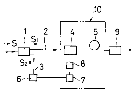
The optical amplification system illustrated in Fig.
1 comprises an optical transmission route constituted by
an optical branching filter 1, an optical transmission
line 2, an optical combiner 4, an optical waveguide 5 and
an optical isolator 9 and a photoelectric conversion route
constituted by the optical branching filter 1, an optical
transmission line 3, a photodetector 6, a drive circuit 7,
a pumping source 8 and the optical combiner 4 and the
optical combiner 4, the optical waveguide 5, the drive
circuit 7 and the pumping source 8 as well as other
components constitute an optical amplifier unit of the
optical amplification system.
The optical branching filter 1 typically comprises a
beam splitter that splits the incoming signal light to a
ratio of, for instance, 1:20.
The optical transmission lines 2, 3 are typically
silicate glass-type covered optical fibers comprising a
core and a clad.
9
2068915
The optical combiner 4 is typically a photocoupler,
e.g., a wave division module (WDF), for combining signal
light and pumped light.
The optical waveguide 5 for optical amplification is
typically a silicate glass- or fluoride glass-type single
mode optical fiber comprising a core and a clad and coated
with a plastic material.
The core o-f the optical waveguide 5 is made of
silicate- or fluoride-type host glass to which one ore
more than one rare earth elements such as erbium (Er) and
praseodymium (Pr) are added. Additionally, one ore more
than one substances selected from a group of substances
including alkaline earth elements such as beryllium (Be),
oxides of yittrium-aluminum-garnet (YAG) crystals, oxides
of yittrium-lanthanide-fluorine (YLF) crystals, transition
metal ions may be added to the host glass.
Alternatively, the core of the optical waveguide 5
may be made of fluoride glass of an erbium-doped ZBLAN
(ZrF4-BaF2-LaF3-NaF) type or containing independently
BaF2, AlF3 and/or NdF3.
The clad of the optical waveguide 5 is also made of
silicate- or fluoride-type glass containing one or more
than one doping substances as described above and
obviously has a refractive index smaller than that of the
core.
2068915
The detector 6 is of a known type comprising
photodiodes (PD) and the drive circuit 7 is an appropriate
electric circuit incorporating a commercial power supply.
The pumping source 8 typically comprises a
semiconductor laser capable of oscillating to emit light
with a required frequency band which is absorption
frequency band of the dopant material (Er, Pr, ...) such
as a 0.8um band, 0.98pm band or 1.48~m band in the case of
Er dopant.
The optical isolator 9 is an optical device having no
polarization sensitivity that can effectively suppress
oscillation of the amplifier (optical waveguide 5) due to
reflection of light or some other cause.
The optical amplification system as illustrated in
Fig. 1 operates to amplify optical signals in a manner as
described below.
Referring to Fig. 1, an incoming optical signal s is
divided into two optical signals si and s2 (sl:s2 - 20:1)
by the optical branching filter I. Thereafter, the two
optical signals sl and s2 are led to their respective
optical transmission lines 2, 3 and then the former
proceeds to the optical waveguide (Er3+ doped optical
fiber) 5 by way of the optical combiner 4 while the latter
is converted to an electric signal by the photodetector 6
and led to the drive circuit 7.
11
2068975
The arive circuit 7 is activated only when it
receives an electric signal from the photodetector 6 to
drive (turn on) the pumping source 8 and remains inactive
as long as it does not receive any electric signal from
the photodetector 8 to leave the pumping source 8 also
inactive.
As the pumping source 8 driven to operate by the
drive circuit 7, it emits pumped light which is led to the
optical waveguide 5 by way of the optical combiner 4.
Under this condition, since the relaxation time of
pumped electrons,is approximately l0ms, activation of the
optical amplification system is delayed by this time span.
If necessary, it may be delayed further by using the drive
circuit 7.
As the optical amplification system of Fig. 1
operates in the above described manner, it does not
amplify the optical signal sl at the rising edge in the
optical waveguide 5 and starts amplifying the signal s1
only slightly after the rising edge is gone.
Consequently, the optical amplification system is
free from the problem described earlier and performs its
expected proper operations.
Fig. 2 is a graph of the waveform of an optical
signal obtained when an optical amplification system as
illustrated in Fig. 1 is used for a line switching system
12
2068975
and before the signal is amplified.
Comparing Fig. 2 and Fig. 10(B), it is clear that the
optical amplification system of Fig. 1 does not respond to
the rising edge of the incoming optical signal.
Fig. 3 is a block diagram of the first embodiment, to
which certain modifications are made.
In this modified embodiment, a bias power source 11
is connected to the pumping source 7 of the optical
amplifier unit 10 in order to enhance the responsiveness
of the optical waveguide 5 for optical amplification.
With this arrangement, since the pumping source 8 is
constantly ready to play its role in optical amplification
at a low level as it receives a bias current from the bias
power source 11 even when no optical signal s2 is applied
thereto and therefore the drive circuit 7 remains
inactive, the optical waveguide 5 can perform an operation
of optical amplification using the excitation energy
supplied from the bias power source lI in advance even if
there is a delay of arrival of pumped light from the
pumping source 8 driven by the drive circuit 7 which is
activated by an optical signal s2. Thus, this modified
embodiment can starts an operation of optical
amplification simultaneously with the rising edge of an
incoming optical signal sl without missing any initial
parts of the optical signal.
13
2068915
While auxiliary pumped light generated when a bias
current is applied to the pumping source 8 has a wave-
length identical with or very close to that of principal
pumped light, its output level is by far lower than that
of the principal pumped light because the optical
waveguide 5 is only weekly excited.
Now, a second embodiment of the invention will be
described by referring to Fig. 4.
An optical amplification system as illustrated in
Fig. 4 differs from the one show in Fig. 1 only in that
its optical amplifier unit 10 additionally comprises an
optical switch 12 and its photodetector 6 is connected to
the optical switch 12, while its remaining technical
features is essentially same as those of the first
embodiment.
In the optical amplification system of Fig. 4, the
pumping light 8 is constantly kept in an on-state whereas
the optical switch 12 is kept in an off-state by the
photodetector 6 as long as there is no optical signal s in
the system.
As an incoming optical signal s is detected in the
system, the optical branching filter 1 divides it into two
optical signals s1 and s2, which are then led to the
respective optical transmission lines 2 and 3. The former
signal sl is then sent to the optical waveguide 5 by way
14
2068915
of the optical combiner 4, while the latter signal s2 is
converted to an electric signal by the photodetector 6 and
applied to the optical switch 12.
As the optical switch 12 is turned on by the control
optical signal s2 transmitted from the photodetector 6, it
allows pumped light from the pumping source 8 to enter the
optical waveguide 5 by way of the optical combiner 4.
Note that, in this embodiment again, the photo-
detector 6 is activated by a control optical signal s2 so
that pumped light reaches the optical waveguide 5 behind
the incoming optical signal sl with a delay of time
required for switching the optical switch 12 by a
detection signal from the photodetector 6.
Thus, the optical amplification system of Fig. 4 does
not amplify the rising edge of the optical signal sl
entered into the optical waveguide 5 and starts amplifying
the signal sl only slightly after the rising edge is gone
and, therefore, it is free from the problem described
earlier and performs its expected proper operations.
Fig. 5 is a block diagram of an embodiment obtained
by modifying the second embodiment.
In this modified embodiment, the optical
amplification system 10 additionally comprises an
auxiliary pumping source 13 and a drive circuit 14 for it
in order to enhance its responsiveness for optical
2068915
amplification, which pumping source 13 and drive circuit
14 are connected between the optical combiner 4 and the
optical switch 12.
With this arrangement, since the optical waveguide 5
is constantly held to a weakly excited state by means of
the pumping source 13 which is driven for an output level
lower than that of normal operation, the optical waveguide
can be readily brought to a highly excited state as in
the case of Fig. 3 as soon as an optical signal sl is
introduced to the optical waveguide 5 and pumped light is
subsequently led to the optical waveguide 5 from the
pumping source 8 as the optical switch 12 is turned on by
a corresponding optical signal s2.
In this embodiment again, while auxiliary pumped
light generated when a bias current is applied to the
pumping source 8 has a wavelength identical with or very
close to that of principal pumped light, its output level
is by far lower than that of the principal pumped light
because the optical waveguide 5 is only weekly excited.
A third embodiment of the invention will be described
by referring to Fig. 6.
An optical amplification system as illustrated in
Fig. 6 differs from those of Figs. 1 and 4 in that an
auxiliary unit 18 for pumping light comprising an optical
combiner 15, a pumping source 16 and a drive circuit 17 is
16
2068975
arranged downstream and connected to the optical amplifier
unit 10, while its optical branching filter 1, photo-
detector 6 and optical amplifier unit 10 are identical
with those of the system of Fig. 1 or Fig. 4.
Of the optical combiner 15, pumping source 16 and
drive circuit 17 of the embodiment of Fig. 6 which are
identical or similar to those of the preceding
embodiments, the pumping source 16 is designed to
constantly keep the optical waveguide 5 in a weakly
excited state while the optical combiner 15 receives
incident light directed reversely relative to the
direction of transmission of signal light.
The optical amplifier unit 10 the optical
amplification system of Fig. 6 operates under the control
of a control optical signal sl in a manner similar to that
of its counterparts in Figs. 1 and 4.
With this arrangement again, since the optical wave-
guide 5 is constantly held to a weakly excited state by
means of the pumping source 13 which is driven for an
output level lower than that of normal operation, the
optical waveguide 5 can be readily brought to a highly
excited state as in the case of Fig. 3 or Fig. 5.
The embodiment of Fig. 6 may be so modified that the
auxiliary unit 18 for pumping light is arranged upstream
and connected to the optical amplifier unit 10.
17
2068915
With such a modified arrangement, the optical
combiner 15 receives incident light coming in the
direction of transmission of signal light.
A fourth embodiment of the invention will be
described by referring to Fig. 7.
An optical amplification system as illustrated in
Fig. 7 differs from those of Figs. 1 and 4 in that an
auxiliary unit 23 for optical amplification comprising an
optical combiner 19, a optical waveguide 20, a pumping
source 21 and a drive circuit 22 is arranged upstream and
connected to the optical amplifier unit 10, while its
optical branching filter 1, photodetector 6 and optical
amplifier unit 10 are identical with those of the system
of Fig. 1 or Fig. 4.
Of the optical combiner 19, optical waveguide 20,
pumping source 2I and drive circuit 22 of the embodiment
of Fig. 6 which are identical or similar to those of the
preceding embodiments, the pumping source 21 is designed
to constantly keep the optical waveguide 5 in a weakly
excited state.
An incoming optical signal s introduced to the
optical amplification system of Fig. 7 is divided into two
optical signals sl and s2 by the optical branching filter
1, which are then led to the respective optical
transmission lines 2 and 3. The former signal sl is then
18
2068915
sent to the optical waveguide 5 by way of the optical
combiner 19, the optical waveguide 20 and the optical
combiner 4 while the latter signal s2 is converted to an
electric signal by the photodetector 6 and applied to the
drive signal 7 of the optical amplifier unit 10 or the
optical switch 12.
The embodiment of Fig. 7 may be so modified that the
auxiliary unit 23 for optical amplification is arranged
downstream and connected to the optical amplifier unit 10.
With such a modified arrangement, the optical combiner 19
receives incident light coming in reversely to the
direction of transmission of the optical signal sl.
A fifth embodiment of the invention will be described
by referring to Fig. 8.
An optical amplification system as illustrated in
Fig. 8 comprises an optical transmission route constituted by
an optical branching filter 1, an optical transmission
line 2, an optical switch 24, an optical waveguide 5 and
an optical isolator 9 and a photoelectric conversion route
constituted by the optical branching filter 1, an optical
transmission line 3, a photodetector 6 and an optical
switch 24, which optical switch 24 is connected to a dummy
signal light source 25.
The optical waveguide 5, the pumping source 8, the
drive circuit 7 constitute an optical amplifier unit 10
19
2068975
while the optical switch 24, the dummy signal light source
25 and the drive circuit 26 constitute an optical dummy
unit 27.
The dummy signal light source 25 generates dummy
signal light in the form of pulse light or continuous
light having a wavelength equal to or close to that of the
signal light s when it is driven by the drive circuit 26.
The inside of the optical waveguide 5 of the optical
amplification system of Fig. 8 is held to a steadily
excited state by the pumping source 8.
As long as no signal light s is applied to the
optical amplification system, the optical switch 24 is
closed at the contacts a and c so that dummy light signal
s3 is fed to the optical waveguide 5 by way of the optical
switch 24.
Theref ore, if, f or instance, there is no signal light
s with 100KH bits or more for a considerable period of
time exceeding several milliseconds, the optical waveguide
keeps on operating under a saturated condition,
constantly amplifying dummy signal light s3.
When signal light s is fed to the optical
amplification system, the light signal s divided into two
signal lights s1 and s2 by the optical branching filter 1,
which are then transmitted through the respective optical
transmission lines 2 and 3.
2068915
The signal light s2 transmitted through the optical
transmission Line 3 is detected and converted to an
electric signal by the photodetector 6, which electric
signal is then applied to the optical switch 24 to close
the contacts b and c, when the signal sl is introduced to
the optical waveguide 5 which is under an excited state so
that the signal s1 is properly amplified.
In other words, the optical waveguide 5 of the
optical amplification system of Fig. 8 operates under a
saturated condition, constantly amplifying dummy signal
light s3 so that it can easily adapt itself to normal
optical signal s1 that comes in to replace dummy signal
light s3.
It may be needless to say that this optical
amplification system does not respond either to the rising
edge of an incoming optical signal sl.
The embodiment of Fig. 8 may be so modified that the
optical dummy unit 27 is arranged downstream and connected
to the optical amplifier unit 10.
More specifically, the optical dummy unit 27 is
connected to the optical amplifier unit 10 by way of an
optical combiner (as in the case of the preceding
embodiment) for receiving incident light directed
reversely relative to the direction of transmission of
signal light sl.
21
2068975
Well known backward excitation techniques and/or
double side excitation techniques may be appropriately
used for the purpose of the present invention in order to
pump light from the fluorescent substance in the optical
waveguide 5.
For receiving signal light s and pumped light by the
optical amplifier unit 10 of an optical amplification
system according to the invention, the signal light s may
be delayed relative to the pumped light before they are
fed to the optical waveguide 5.
As it may be clear from the above description, a
condition where no light signal is entered into an optical
waveguide of an optical amplification system refers, for
the purpose of the present invention, to cases where the
existing signal light is interrupted or a succeeding
signal light is not entered into the waveguide for a
predetermined period of time after a preceding signal
light is gone.
Since an optical amplification system according to
the invention does not operate for optical amplification
at the rising edge of an incoming optical signal and hence
its operation is not affected by the waveform of the
optical signal, it is free from the risk of destructing
downstream systems and/or giving rise to a saturated state
to make it a safe and stable system.
22