Note : Les descriptions sont présentées dans la langue officielle dans laquelle elles ont été soumises.
2069142
-
FIELD OF THE INVENTION:
This invention relates to telephony, and in
particular to a digital receiver for receiving data sent
by a Stored Program Control Switching System (SPCS)
usually called CLASS messages.
BACKGROUND TO THE INVENTION:
CLASS messages are usually transmitted over a
voice transmission path during the silent interval
between the first and second power ringing signals, to
customer premises equipment (CPE). The transmission
scheme used is analog, phase-coherent frequency shift
keying (FSK) with logical l's (marks) modulated by
1200 + 12 Hz and logical 0's (spaces) modulated by
2200 + 22 Hz. This binary data is sent serially in an
asynchronous way at a rate of 1200 bits per second (1200
baud).
Typically, a peripheral of the CPE receiving
the data uses a digital to analog (D/A) converter called
a CODEC. CODECs which sample analog signals at a fixed
rate of 8,000 Hz are relatively inexpensive and are
consequently preferred over more complex CODECs having
selectable sampling rates. The output of the CODEC is a
compounded 8 bit value which could be expanded (in
hardware or software) to a linear value with one sign
bit and 12 bits (for Europe) or 13 bits (for North
America) for magnitude.
SUMMARY OF THE INVENTION:
The present invention is a class message
receiver that in one embodiment can be implemented in a
Digital Signal Processor, and which can extract the data
from a signal sampled at 8,000 Hz.
The present invention demodulates the FSK
modulated data, ensures that the data has been received
in conditions specified by telephony standards, and
-2- 206~1~2
_
verifies the data using an error detection mechanism
provided for the transmission of class messages.
An FSK demodulator takes input linear samples
of the signal and filters them with a bandpass filter
which does an upsampling to increase the sampling rate
from 8,000 Hz to 24,000 Hz, which results in 20 samples
at the output of the bandpass filter for each incoming
data bit. The amplitude of the signal/samples at the
output of the bandpass filter is adjusted by an
automatic gain control (AGC) circuit and the resulting
samples (for convenience referred as sample (t), where t
is a discrete moment in time) are processed along two
different paths designed to estimate the likelihood of
the input signal encoding a mark (mark estimation path)
or a space (space estimation path). This "likelihood"
is quantitatively represented by a value called ML (most
likelihood) estimator which is calculated at the end of
each of the two paths based on the formulae:
M2(~i) = X2(~i) + Z2(~i)
t=to+l9
where X(~ sample(t) cos(~it)
t=to
t=to+l9
and Z(~i) ~ sample(t) sin(~it)
t=to
where ~i is either ~m (1200 Hz) for the mark
path or ~5 (2200 Hz) for the space path.
The outputs of the estimators are provided to
a slicer, and at the output of the slicer to a decision
circuit.
Preferably the two input streams of samples at
the input of the ML estimator (mutually phase shifted by
gOo) for the space estimation path, are provided to a
2069142
baud recovery circuit which operates on every pair of
samples supplied by the two streams. The baud recover
circuit uses 20 sample pairs (the current pair plus the
previous 19 pairs) to calculate the ML estimator for the
space at every increment in time.
The stream of ML estimators calculated by the
baud recovery circuit is low pass filtered, is passed
through a threshold circuit and a differentiator which
provides an output signal when the slope changes its
sign from + to -. The slicer thus is enabled from that
output signal to receive the estimated output values
from the two ML estimator at the end of the two
estimator paths, at particular times which are at the
peak of marks or spaces.
The output of the slicer is provided to a
decision circuit. A decision as to whether a mark or a
space is present is made by the decision circuit, at the
instant of slicing, which is at the center of a bit.
The resulting decoded bit is saved if it
belongs to a character being received or it is discarded
if it is a carrier bit between two successive
characters. When a full character (1 start bit + 8 data
bits + 1 stop bit) has been received, the start bit and
the stop bit are discarded and the remaining character
is saved in a buffer. The last character of a message
is a check sum which when added modulo 256 to the
previously received characters of the message should
result in the combined value 0. If the sum is not zero
the whole message is discarded.
More generally, in accordance with the
preferred embodiment of the invention, a frequency shift
keyed receiver is comprised of apparatus for receiving a
demodulated frequency shift keyed sampled sequence of
data bits which is frequency shift keyed by upper and
lower frequencies ~5 and ~m apparatus for encoding the
20691~2
-4-
-
received sequence with pairs of 9o phase shifted
signals of upper frequency ~s of the frequency shift
keyed sequence and lower frequency ~m of the frequency
shift keyed sampled sequence resulting in a pair of
S mutually 90 phase shifted sampled sequence signals
encoded by ~5 and a pair of mutually 90 phase shifted
sampled sequence signals encoded by ~m~ a pair of most
likely (ML) estimators each for receiving the respective
pairs of signals and for continuously operating on the
signals to obtain a pair of output signals one
representing the likelihood of the upper frequency and
one representing the likelihood of the lower frequency
sequence having a data bit present, a baud recovery
circuit for determining the timing of a mark or space
bit and for providing an enable signal corresponding to
the timing thereof, a slicer for receiving the output
signals and the enable signal and providing amplitude
levels of the output signals of the estimators at an
input to a decision circuit when enabled, the decision
circuit for indicating the higher amplitude one of the
estimated output signals.
In accordance with another embodiment
a frequency shift keyed receiver is comprised of
apparatus for receiving a demodulated frequency shift
keyed sampled sequence of mark and space data bits,
apparatus for separately operating on 90 phase shifted
pairs of the data bits by a process
M2(~i) = X2(~i) + Z2(~i)
t=to+ 1 9
where X(~ sample(t)-cos(~it)
t=to
t=totl9
and Z(~ sample(t) sin(~it)
t=to
~ -5- 20691 ~2
in which ~i is ~m and ~s in separate operations, to
provide a pair of mark and space estimated signals,
apparatus for low pass filtering one of the mark and
space estimated signals, apparatus for low pass
filtering and differentiating the one signal to obtain a
slicer enable signal, slicer apparatus for receiving the
estimated signals, and for receiving the enable signal,
whereby a slice of the estimated signals at the time of
the enable signal is provided at an output, a decision
circuit for receiving a slice of the estimated signals,
for determining which of the estimated signals is the
greater and for providing an indication of the presence
of a mark or space bit thereby.
It should be recognized that the term "signal"
refers to a digital value (sample), unless specified as
an analog signal, since the present invention relates to
a digital receiver.
BRIEF INTRODUCTION TO THE DRAWINGS:
A better understanding of the invention will
be obtained by reference to the detailed description
below, in conjunction with the following drawings, in
which:
Figure 1 illustrates the form of a typical
class message,
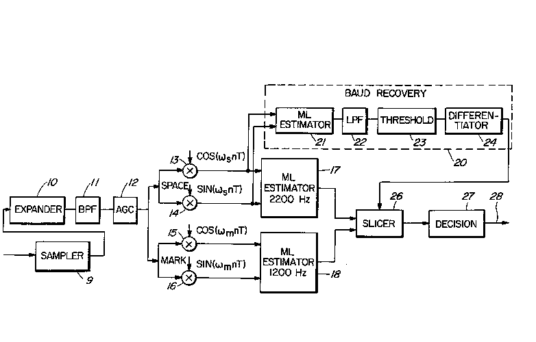
Figure 2 is a block diagram of the invention,
Figures 3A and 3B are plots of the mark and
space signals respectively at the outputs of the pair of
ML estimators, and
Figures 4A and 4B are plots of the mark and
space signals respectively either of which is used,
after further processing, to enable the slicer in Figure
2.
DETAILED DESCRIPTION OF THE INVENTION:
Figure 1 illustrates schematically a
representative form of a class signal. It is typically
2069142
comprised of a first sequence 1 of bits which sequence
is of the form "01010101" for about 250 msec. This
signal is used to aid the baud recovery process of a
frequency shift keyed (FSK) demodulator, which typically
is activated by a 1 to 0 transition. The class
signalling scheme typically uses analog, phase-coherent
FSK signals for transmission.
An immediately following second data sequence
2 is comprised of a 150 + 25 msec group of l's. This
sequence facilitates adjustment an automatic gain
control of the receiver during this period.
All subsequent sequences are preceded by a 0
and terminated by a 1, and constitute the class message
itself.
The first sequence of the class message, i.e.
the third data sequence 3 defines the message type, the
fourth data sequence 4 defines the message length, and
all subsequent sequences 5 except the last define data.
The final sequence 6 defines a check sum for the
preceding sequences. Each sequence is preferably an
eight bit data byte bounded by the aforenoted 0 (space)
start bit and a 1 (mark) stop bit.
An inter-byte sequence 7 of marks (l's) is
sent between consecutive bytes of a length sufficient to
ensure that the maximum interrupt time between two
consecutive bytes is no longer than preferably 16.7
msec, and to allow checking that the mark signal is not
interrupted for more than 8 msec.
Consequently the receiver first indicates the
presence of the first sequence 1, for initialization,
then detects the second sequence 2, during which time
the AGC of the receiver adjusts its gain factor. The
class message itself is then received, first the message
type, then the message length, then the data bytes, then
the check sum, in an asynchronous protocol as described.
2069142
-7-
-
The class receiver preferably also checks the presence
of the inter-byte carrier, to ensure that the maximum
interrupt time between two successive bytes is no longer
than 16.7 msec and that the mark signal is not
S interrupted for more than 8 msec. The data is then
evaluated against the check sum for validity in a well
known manner.
The above description depends on the ability
of the receiver to extract the sequence of 0's and l's
from the received signal. A block diagram of a system
to extract the sequence is described with reference to
Figure 2.
The input of the receiver is supplied by a
sampler 9 (a CODEC) which samples the frequency shift
keyed modulated sequence at a rate of e.g. 8,000 Hz (the
rate of an inexpensive fixed rate CODEC), and passes it
through an expander 10, the output of which is used by
the receiver. This sampling rate is not an integral
multiple of the baud rate, e.g. 1,200 baud, an example
baud rate of the signal referred to above and shown in
Figure 1. The signal is comprised of mark and space
signals, the mark signal being at 1,200 Hz and the space
signal at 2,200 Hz. The output signal of expander 10 is
provided to digital bandpass filter 11 which limits the
input signal to the range between 1.1 kHz and 2.3 kHz.
This digital filter increases the sampling rate by a
factor of 3 to 24,000 Hz, which is a multiple of 1,200
and of 8,000. If the sample rate were not to be
increased (e.g. if the 8,000 Hz sampling rate were an
integral multiple of 1,200 Hz), then instead of the
bandpass filter 11 increasing the sampling rate to a
frequency which is an integral factor of the baud rate
and sampler 9 sampling rate, a "FIR" filter with fewer
coefficients would suffice for the bandpass filter.
When a FIR filter is used, the group delay at both
2û~9142
-8-
-
encoding frequencies (wm = 1,200 Hz and ~5 = 2,200 Hz) is
the same.
The parameters of the FIR digital filter in a
laboratory prototype successful embodiment were:
sampling frequency: 24,000 Hz,
number of coefficients: 59
stop band cut-off frequencies: 800 Hz and
2,600 Hz,
pass band cut-off frequencies: 1,100 Hz and
2,300 Hz,
ripple in dB in first stop band: -9.976 dB,
ripple in dB in second stop band: -9.944 dB,
ripple in dB in the pass band: .271 dB.
At 24,000 Hz, twenty samples per baud was
used.
The output signal of the bandpass filter is
applied to an automatic gain control circuit 12 which
calculates a gain control factor based on the average of
the maximum absolute value of the last twenty samples of
the output of the bandpass filter and on a predetermined
desirable range of signal amplitudes. The gain control
factor is preferably recalculated every sixty samples
(and is used as such for the next sixty samples).
The output signal of the AGC circuit is
applied to space bit multipliers 13 and 14 and mark bit
multipliers 15 and 16. In the space bit multipliers 13
and 14 each input signal thereto is respectively
multiplied by 9oo phase shifted samples of 2,200 Hz,
shown as cos (~snT) and sin (wsnT) respectively. The
input signal is also multiplied in multipliers 15 and 16
with corresponding mutually 90 phase-shifted 1,200 Hz
samples cos (wmnT) and sin (~snT) respectively. The
output of each pair of multiplexers is applied to a
corresponding ML estimator 17 and 18.
2069142
g
Each ML estimator processes the input signals
thereto in accordance with the following algorithm:
M2(~i) = X2(~i) + Z2(~i)
s
t=to+ 1 9
where X(~ sample(t) cos(~it)
t=to
t=to+l9
and Z(~ sample(t) sin(~it)
t=to
where ~i represents the mark frequency ~m
(1,200 Hz) or space frequency ~s (2,200 HZ).
Figures 3A and 3B are plots representing the
amplitudes of the output signals M2(~m) and M2(~s), mark
and space, respectively, over 300 samples. It may be
seen that the plots are jagged. It is the function of
the circuit described below to determine where the
samples should be considered as being in the center of a
bit.
Considering the plots of Figures 3A and 3B, it
should be noticed that M2(~m) reaches its peaks when
M2(~S) reaches its minimums and vice versa. However the
plots show that local maxima and minima exist which make
the decision process of what is the nature of the bit
difficult.
Preferably the orthogonal space signals are
applied to a baud recovery circuit 20, to determine the
preferred precise instant center of the bit. The
signals are applied to a continuous ML estimator 21,
which operates on the signals using the same algorithm
as does ML estimator 17, as described above. The output
of the ML estimator 21, in the form of the signal shown
in Figure 3B, is applied to a low pass filter 22, which
is preferably a fourth order elliptical filter. In a
2069142
~o
.
successful embodiment, the parameters of the low pass
filter 22 included a sampling frequency of 24,000 Hz, a
pass band of 0 - 2.6 kHz with .3967 dB ripple and a stop
band of 3.6 kHz - 12 kHz and ripple of -26.7474 dB.
S A plot of the output signal from low pass
filter 22 is shown in Figure 4B. If the mark signals
had been used to provide baud recovery, a plot of the
resulting output signal of the low pass filter 22 is
shown in Figure 4A.
The output signal of low pass filter 22 is
applied to a threshold circuit 23. It will be seen from
the plot shown in Figure 4B that it is a much simpler
task to determine whether or not the signal is above or
below a threshold, than the plot of Figure 3b.
lS The output of the threshold circuit 23 is
applied to a differentiator 24, which calculates the
slope of the signal passing into it.
It may be seen that if all of the space
signals in Figure 4B are of sufficient amplitude to pass
through the threshold circuit 23, the function of the
differentiator 24 is to determine the exact center of
the bit. The differentiator therefore differentiates
from a + to a - slope, the zero slope value representing
the exact peak 25 of the signals shown in Figure 4B.
The output of differentiator 24 at the time of
the peak 25, is applied to an enable input of a slicer
26. Due to delay in the baud recovery circuit, the
enable input is controlled to be delayed by one bit.
Slicer 26 receives the output signals of estimators 17
and 18, plots of which are shown in Figures 3A and 3B.
Slicer 26 provides a signal to decision circuit 27 at
the exact instant of peak 25. The signals, (an
approximate minimum for the mark ML estimator and an
approximate maximum for the space ML estimator or the
other way around), thus are presented at the correct
2069142
11
-
instant in time of decision circuit 27 for analysis.
The decision circuit determines whether the space ML
estimator is greater than the mark ML estimator, and
thus indicates that by providing a signal at its output
28 that a 0 (space) has been received.
It is preferred that only one of either the
mark or space signals should be analyzed in the ML
estimator 21. However the space signal is preferred to
be used because the start bit of a transmitted byte
(sequence 3, 4, 5 or 6 of Figure 1) is a space (0), and
if an adjustment to an internal clock of the receiver or
of other circuits is required as a result of the
analysis made by this circuit, this will be provided
upon the arrival of a new character. However it will be
understood that this circuit can be used for other
purposes than the class signal receiver application
noted herein, and thus the ML estimation of the mark
signal could be analyzed in place of or in addition to
analysis of the space signal.
It will be recognized that ML estimator 17 may
be used for double duty, i.e. as ML estimator 21. In
that case ML estimator 21 is not used, but the output
signal of ML estimator 17 is additionally provided to
the input of low pass filter 22.
While the above has described the present
invention in hardware terms, the process of operation of
the hardware constitutes an algorithm of method steps,
which may be implemented in software programs or
firmware. Each of the hardware functions may be
implemented by analogous software or firmware programs.
A person understanding this invention may now
conceive of alternative structures and embodiments or
variations of the above. All of those which fall within
the scope of the claims appended hereto are considered
3s to be part of the present invention.