Note : Les descriptions sont présentées dans la langue officielle dans laquelle elles ont été soumises.
~ 2069808
, ,
P/8677/SPECIAL/us
-- 1 --
ANALOGUE-TO-DIGITAL CONVERTERS
This invention relates to analogue-to-digital (A-D)
converters, and especially to sigma-delta
analogue-to-digital converters.
Sigma-delta A-D converters include quantising means
for producing a digital output, oversampled relatlve to the
signal bandwidth, and a feedback loop for feeding back a
signal derived from the digital output to be combined with
the analogue input for input to filter means, the output of
the filter means being connected to the quantising means:
this is in order to shap~ the quantisation noise to reduce
it in a desired bandwidth (GB-A-2,232,023).
A typical implementation of such a sigma-delta
converter is shown in Figure l, this having a second order
filter and bandpass characteristic. Each part o~ the loop
filter consists of parallel resonant circuits o~ an inductor
and capacitor in parallel, ~ C1, I~ C2, in series with
resistors Rl, R2. Buffers l - 3 provide isolation between
the ~ilter stages and between the filter and the quantising
means 4 and between the summing node 5 and the analogue
input. The feedback loop includes a digital-to-analogue
~ 20~98~8
P/8 67 7/SPECIAL/us
converter (D-A) 6.
The amplitude and phase of the voltage across each
stage of the filter is shown in full line in Figures 2a, 2b.
The effect of the series resistors R1, R2 is to add a
uniform step (shown dashed) to the amplitude response (also
shown dashed) of the resonant circuit and, more importantly,
to reduce the phase shift of +90 produced at low and high
freg~encies (the dashed curve showing the phase shift if the
resistors Rl, R~ were replaced by short circuits). The
reduction in phase shift reduces the tendency to instability
which could arise if the combined phase shift of the two
filter stages approached 180, thus turning negative
feedback into positive feedbacX.
A problem with such filter stag~s i8 that thQ buffers
and summing node inherently have input and output
c~pacitance~ to earth which load the tuned circuit. This
degrade~ the Q of the resonant circuits, since some energy
is exchanged between the input and output capacitance and
the inductance Ll via the resistors R1, R2, so that energy
iB dissipated in the resistors. The reduction in the Q
factor reduces the peak of the amplitude response and thus
degrades the notch in the quantisation noise produced by the
sigma-delta modulator and hence the signal-to-noise ratio
2069808
P/8677/SPECIALJUs
which can be achieved.
An analagous problem arises in the case of sigma-delta
converters with series resonant circuits connected in
parallel with resistive means to modify the phase response
of the resonant circuits.
Another problem which is encountered by both band-pass
and base-band sigma-delta A-D converters is that the
presence of resistive means in the first stage of the filter
imposes a certain bandwidth requirement on subsequent filtar
stages.
According to one aspect the invention provides an
analogues-to-digital converter comprising an input ior
analogue signals, quantising means for produ¢ing a digital
output, a ieedback loop for feeding back a signal derived
irom the digital output to be combined with the analogue
input for input to filter means, the filter means including
a stage which comprises a filter circuit which i8 not
c~nected to phase-modifying resistive means, and which is
connected between ground and one input Or a pair of
differential inputs, and resistive means connected between
ground and the other input of the pair of differential
inputs.
206.9~0~
P/8677,~SPECIAL/us
-- 4
In the case of bandpass filter means, the input
capacitance of the means e.g. buffer having the
differential inputs which follows the resonant (filter)
circuit and the output capacitance of the preceding
component e.g. buffer in the feedforward path, now combine
with the capacitance in the resonant circuit in such a way
that the energy no longer passes via any phase-modifying
resistor, thereby improving the Q of the resonant circuit
and the notch shape of the filter. Nevertheless, the effect
at the output of the filter stage referred to is the same as
if the filter stage did include phase-modifying resistive
means, so that the necessary reduction in phase shift from +
90 i~ maintained. The means having the differential inputs
may be a bu~er, but could if desired be the quantising
means itself, or any other component.
According to another aspect, the invention provides an
analogue-to-digital converter comprising an input for
analogue signals, quantising means for producing a digital
output, a feedback loop ~or feeding back a signal derived
from the digital output to be combined with the analogue
input ~or input to filter means, a stage of the filter means
comprising a filter circuit which is not connected to
phase-modifying resistive means, and a signal derived from
2~
P/8677~SPECIAL/us
that stage of the filter means being combined in use with a
signal derived from the digital output, for input to the
quantising means, of the output of the filter means or the
output combined as aforesaid.
The absence of phase-modifying resistive means
connected to the filter circuit provides the same
improvement of the Q and notch shape in the case of a
bandpass filter means as before, and the signal derived from
the digital output that is combined with the signal derived
from the filter stage, has the same effect as the
phase-modifying resistive means provided in the said one
a~pect of the invention, so that the necessary reduction in
phase shift ~rom +90 can be maintained. The combination o~
the signal derived from the stage of the filter means
comprising the filter circuit with the signal derived from
the digital output, may be directly a~ter that stage, but in
the case where the stage i~ the ~irst stage, the combination
could instead be after the signal has passed through a
second or third etc stage. If the combination is after the
only or after a final stage of the filter means, the
quantising means will be fed the combined output referred
to. If the combination is after a first stage of the filter
means, and there is no combination a~ter the ~inal stage o~
the filter means, the quantising means will receive the
2069~08
P/8677/SPECIAL/us
output of the filter means uncombined with any other signal.
In the case of either aspect of the invention, the
absence of the phase-modifying resistive means in a first
stage of the filter means (in either baseband or bandpass
filter means) permits a reduction in bandwidth in subsequent
filter stages, permitting lower power consumption by those
stages.
In the case of either aspect of the invention, the
filter means could comprise a single stage, or two stages,
three stages or a higher number of stages.
The resonant (filter) circuit in the case of bandpass
~ilter mean~ may comprise an inductor and a capacitor, and
may b~ parallel or ~eries, and the filter circuit in the
case of baseband ~ilter means may be an integrating circuit
e.g. capacitive.
The quantising means may include a comparator and, to
avoid this being affected by drift, this may be a.c.
coupled to the preceding stage, or any drift may be
compeneated for by means oi d.c. ~eedback to a stage o~ the
filter means. The d.c. feedback may include an integrator
for integrating the data output, converted to analogue form.
- 2~8~
. P/8677/SPECIAL/us
-- 7 --
The quantising means may be single bit, but could be
multi-bit if desired.
The sampling rate of the quantising means may be four
times the resonant frequency of the resonant circuit but,
since notches in the quantising noise occur at one quarter,
three.~quarters, five quarters etc times the sampling rate,
the ~ampling rate could instead be four thirds times the
resonant frequency, four fifths times, or four sevenths
times etc.
Sigma-delta analogue-to-digital converters constructed
in accordance with the invention will now be described by
way o~ example with reference to the accompanying drawings,
in which:
Figure 3 i8 a block diagram of a first sigma-delta A-D
converter;
Figure 4 shows a modified form of the filter of the
converter of Figure 3 in simplified ~orm together with
voltages acros~ various components in response to a pulse
input;
2~9g~8
. ~
P/8677/SPECIAL/us
Figure 5 is a block diagram of a second sigma-delta
converter, which is a balanced version of the modified form
of the first sigma-delta converter; and
Figure 6 is a block diagram of a third sigma-delta A-D
converter.
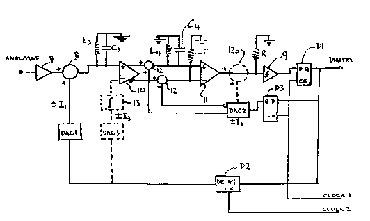
Referring to Figure 3, the first sigma-delta converter
has ~ bandpass characteristic and employs a second order
parallel loop filter. This is tuned to one quarter the
sampling frequency of the quantising means of the sigma
delta converter, and so is suitable for conversion of
signals at this frequency, at which the sigma-delta
converter produces its null in the quantisation noise. If
desired, the ~ilter could be tuned to three quarters, five
quarters, seven quarters etc o~ the sampling frequency. The
sigma-delta converter shown in Figure 3 feeds to decimation
~ilters (not shown) for removing out of band noise and for
reducing the sampling rate.
The analogue voltaqe input is applied to a buffer 7
having a high input impedance and provides an output current
which is applied to a summing node 8. Digital output data
appears at the output of quantising means formed by
comparator 9 and clocked D-type flip-flop Dl, which provides
., ,.. ,~.. ............ . . . . .
2~69808
P/8677/SPECIAL/us
one bit data voltage samples, (which could be current
samples if desired) from the Q output, the output of
comparator 9 being transferred to the D input of the D-type
flip-flop Dl and from the D input to the Q output on each
clock pulse. The data is stored for one sample period at
the Q output of flip-flop Dl before being latched by both
flip-flops D2 and D3.
- A feedback loop which includes digital delay D2 (e.g.
D-type flip-flop providing a one clock pulse delay) feeds
the data pulses to digital-to-analogue converter DACl which
provides current pulses (of +I1) which is summed with the
analogue input current at summing node 8. The delay is
clocked at the same rate but not necessarily at the same
phase as flip-flops D2 and D3. A delay o~ two clock periods
between data being sampled and that data being reproduced by
DACl is equal to 180 of phase shift o~ the analogue signal
at the resonant frequency of the resonant circuit, and since
at the resonant frequency, the loop filter has no phase
shift, the summation at the summing node 8 is equivalent to
negative ~eedback which is of course necessary for
stability.
Buffer amplifier lO of high input and high output
impedance monitors the voltage across the first stage of the
20~9808
P/8677/SPECIAL/us
-- 10 --
filter comprising inductor ~ and capacitor C3 in parallel,
which is connected without any phase-modifying series
resistance between the input to the buffer and ground. The
buffer provides a differential output current (i.e. two
current outputs equal in magnitude and opposite in sign) to
summing nodes 12 connected to its inverting and
non-inverting outputs. The summing nodes 12 also receive an
analogue version of the digital output (+I2) via a
digital-to-analogue converter DAC2. This current is delayed
by one clock period due to D-type flip-flop D3 (the D-type
flip-flop Dl having stored the data for a one period delay).
Thus, the signal generated by DAC2 and applied to the
summing nodes 12 will affect the signal sampled at the
D-type flip-flop Dl at the sampling instant which is two
sampling instants later than that when the data was ~irst
sampled.
Buffer amplifier 11 of high input impedance and high
output impedance monitors the voltage across the second
stage of the ~ilter comprising inductor I4 and capacitor C4
in parallel without any phase-modifying series resistance,
and across resistor r. The parallel inductor and capacitor
are connected between the non-inverting input and ground,
and the resistor is connected between the inverting input
and ground. The output current from the buffer amplifier is
20~9~8
P/8677/SPECIAL/us
converted to a voltage at the comparator input by means of
resistor R.
According to one aspect of the invention, the second
stage of the filter has the same effect regarding reduction
of phase shift from +90 as in the prior art arrangement
shown in Figure 1 i.e. it has the amplitude and phase
characteristics shown in full line in Figures 2a, 2b while
avoiding the detrimental effects of input capacitance to
ground on the Q of that stage of the filter. Thus, the
¢urrent output of say buffer amplifier 3 in the prior art
arrangement shown in Figure 1 is the product of the voltage
acro~ , C2, R2 and the transconductance of the buffer
ampli~ier. The voltage across I7, C2, R2 i8 the product of
the current through L2, C2, and its impedance, together with
the product of the current through ~2 (the same current) and
it~ impedance. It is apparent that the buffer amplifier 11
in Figure 3 will produce the same output current for the
same vaIues L C R, transconductance and input signals
values. This is because the voltages across 14, C~ will be
the ~ame as the voltage across I~, C2, and the voltage
across r will be the same as the voltage across R2 (the two
current outputs of buffer amplifier 10 being of equal
magnitude), and the effect of the inverted signal at the
inverting input will be such that the two voltages are
2~9808
P/8677/SPECIAL/us
summed. The resistance r produces the flat dashed response
shown in Figure 2 and the parallel resonant circuit L4, C4
produces the dashed resonant response, the two curves being
summed as before to produce the effect shown in full line.
As far as the phase response is concerned, the series
resistor r will predominate over the effect of the
inductance at low frequencies and the capacitance at high
frequencies and the full line curve will again be produced.
The output capacitance to ground of the buffer
amplifier 10 and the input capacitance to ground of the
buffer amplifier 11 will sum with the capacitance C4
allowing these quantities to be taken into account when
choosing C~, but the resonant current through C~ will not
pa~ through r and degrade the Q o~ the filter. It should
be mentioned that any inter-terminal capacitance of the
buffer amplifier will degrade Q, ~ince this will still load
the resonant circuit through r, but inter-terminal
capacitance i~ not such a serious problem as capacitance to
ground.
The arrangement described for the second stage of the
filter may equally be applied to the first stage, and to any
or all of any other stages, or to the case of a filter
having a single stage only. If desired, the buffer
....... .... .. ~ . . . . . .
20698~8
P/8677/SPECIAL/us
-- 13 --
amplifier 11 may be dispensed with, provided that high
impedance differential inputs are provided at the comparator
9 of the quantising means.
According to another aspect of the invention, the
effect of the series resistor r is produced by a signal
derived from the digital output, in this case, the current
from the digital-to-analogue converter DAC2. This current
iB added to the output of the buffer amplifier 10 at summing
nodes 12.
The current from DAC2 is designed to produce the
effect of a resistor connected between ground and the
im erting input of buffer amplifier 10. The amplitude and
pha~ re~ponse of I3, C3 is as shown in broken line in
~igure 2a, 2b. In the ~ame way that resistor r in the
~econd ~tage produced a particular current in the output of
bu~fer a~plifier 11, DAC2 provides an identical current in
the output of buffer amplifier 10, in non-inverted and
inverted form because the buffer amplifier has differential
outputs. The effect on the amplitude response of the first
~tage of the filter i~ to add the dashed flat response to
produce the full line amplitude and phase response shown in
Pigures 2a, 2b.
,,,,,; . ~, .,, ., .,,, ., . j . .. ..... .. . . .... .. , ., , .. .... ..... ~
2~9~8
P/8677/SPECIAL/us
- 14 -
Thus, the advantages of a resistor similar to the
resistor r in the second stage can be achieved in the first
stage of the filter by providing differential
digital-to-analogue converters which receive an input from
the data output. Equally, the advantages of the resistor r
itself in the second stage could be achieved by a
digital-to-analogue converter connected to a summing node at
the output of the second stage, and the same would apply to
any further stages or to just a single stage. Indeed, the
third sigma-delta A-D converter described (Figure 5) is of
this type.
The possibility also exists, and this is illustrated
by dotted line connection to summing mode 12a provided in
pla¢e o~ summing nodes 12 in Figure 3, of simulating a
series resistor for the first filter stage by a
digital-to-analogue converter connected to the output of the
second filter stage. However, in this case, the loss of the
resistor from the first stage also requires an increase in
resistance r in the second stage to provide full
equivalence. This can be appreciated by reference to Figure
4, which shows a simplified version of the filter of Figure
3, with each stage consisting of a parallel inductor and
capacitor ~C3, L4C4 connected between ground and one input
of the differential amplifiers 10, 11, and a resistor r1, r2
, .. . . .. . ..
2~69~08
P/8677/SPECIAL/us
- 15 -
connected between ground and the other input of the
differential amplifier.
At the first stage, input current pulse I produces a
voltage pulse Vr1 across resistor rl and a voltage VL3c3
across L3C3 which rises sharply during the current pulse and
continues sinusoidally thereafter.
: Each voltage Vrl, VL3~ produces a voltage across each
of r2 and L4C4. Thus, the voltage across r2 consists of a
voltage pulse due to Vrl and a voltage due to VL3c3. The
voltage across L~C4 consists of a voltage due to Vrl,
sharply increasing during the pulse Vr1 and thereafter
continuing sinusoidally, together with an increasing
sinusoidal voltage due to VL3C3.
Thus, if resistor r1 is omitted, and pulses from DAC2
are summed with the output from dif~erential amplifier 11,
the voltage across L4C~ due to resistor rl must be
compensated for, and this is done by increasing r2 (the
resistor r in Figure 3) since the voltage signal across r2
due to L3C3 i8 of the same form as rl would have produced
aCrOSB L4C4. The pulse part of Vr2 is of course provided by
DAC2.
... ......... .... .
2069808
P/8677/SPECIAL/us
- 16 -
The comparator 9 operates by assessing whether its
input voltage lies above or below a certain threshold. It
will be apparent that incorrect results will be obtained if
drift occurs in any of the preceding components i.e. buffer
amplifiers 10, 11 or adders 8, 12. An offset could be
applied to the comparator and an output from the amplifier
11 smaller than this offset could be masked by the offset
and produce an incorrect output from the comparator. To
overcome this, the comparator may be a.c. coupled i.e.
connected to buffer 11 via a capacitor. Another alternative
i8 indicated by digital-to-analogue converter DAC3 and
integrator 13. The digital output, reconverted to analogue
form, i~ integrated in integrator 13, and is applied to
inverting input of buf~er ampli~ier 10 to tend to compensate
for any offset applied to comparator 9, so that the time
averaged output of the digital output has zero d.c. level.
While the quantising means is single bit, multi-bit
quanti~ation may be employed if desired.
Pigure 5 shows the circuit of Figure 3, in the
modified $orm in which DAC2 feeds summing node 12a in place
o~ summing nodes 12, in balanced ~orm. Like parts have been
given like reference numerals. Feedback pulses
corresponding to those provided by DACl and DAC2 are now
20~9~08
P/8677/SPECIAL/us
provided by current generators Il, I2 which are applied to
either the inverting or non-inverting lines via DAC
controllers 14, 15, the line selected being chosen by the
data. Capacitance IS is earthed at the centre and tapped at
two points between the centre and its ends. DAC3 and
integrator 13 may be provided, a buffer 13a providing
inverting and non-inverting outputs.
_ As mentioned above, the Figure 3 converter may be
modi~ied by substituting resistor r with digital-to-analogue
converters at the output of both stages of the filter, and
such an arrangement is illustrated in Figure 6. Again, like
re~erence numerals have been used for like parts. The
arrangemQnt i~ unbalan¢ed, and an additional adder 16 is
provided. DACl provides the normal feedback pulses ~or the
~igma-delta converter via a delay clocked at the same
~requency but not necessarily at the same phase as
~lip-~lop~ Dl, D3. DAC2a provides pulses which simulate the
e~ect o~ resistor r in Figure 3 but ~or the ~irst stage o~
the filter. DAC2b enables resistor r in the second stage o~
the ~ilter to be oDitted. Referring to Figure 4, it will be
apparent that DAC2a and DAC2b do not provided complete
compensation for the omitted resistors. Thus, while DAC2a
is fully equivalent to resistor rl, DAC2b is not ~ully
equivalent to resistor r2, since there will be no equivalent
,, ",", ~j~"""""", , ,,, ,,, , ,, ,, , ",.. . . . . . ........
2~6~808
P/8677/SPECIAL/us
- 18 -
for the effect of the voltage across I~C3 on r2. This is
compensated for by increasing the signal from DAC2a over and
above what is required for DAC2a to produce the same effect
in the output of buffer amplifier 10 as resistor rl. This
is possible since the increased effect of DAC2a on L4C4 will
be the same as the effect ISC3 would have had on omitted
resistor r2. DAC2b compensates for the effect of omitted
resistor r1 on the omitted resistor r2.
-
Modifications may of course be made without departingfrom the scope of the invention. Thus, instead of
monitoring the voltage across parallel resonant circuits
(without series resistive means) and presenting an output
voltage to the comparator, the current through series
resonant circuits ~without parallel resistive means) could
be monitored, and a current could be presented to the
comparator. Equally, ceramic resonators could be employed
as resonant circuits as an alternative to inductive
capacitative filters. Finally, all the embodiments of
Figures 4 to 6 could be baseband instead of bandpass
implementations i.e. the resonant filter circuits could be
integrating filter circuits i.e. capacitors.
, .:. ,.. , . ,.. , .. ~ .. , .. ,, .~ ., . . -.. . .