Note : Les descriptions sont présentées dans la langue officielle dans laquelle elles ont été soumises.
' -
Apparatus and Method for
5Detecting Intermodulation Distortion
in a Radio Frequency Receiver
Field of the Invention
The present invention relates generally to
receivers, and more particularly to detecting
intermodulation distortion in a radiotelephone receiver.
15Background of the Invention
A radio frequency (RF) receiving device, of which a
cellular radiotelephone mobile subscriber unit is a
convenient example, provides an appropriate setting for
20 describing the need for the present invention.
Subscriber units are designed to operate with all
cellular systems (for example: A or B) that provide
competing services in a particular geographical area.
Each system is assigned a number of channels with a
25 particular channel spacing and each channel has a
particular center frequency as called out in Electronic
Industries Association (EIA)-553, 2.1.1.1 "Mobile
Station - Land Station Compatibility Specification". The
subscriber unit gains access to the system in which it is
30 registered, System A for example, by scanning the
access channels to determine the strongest two access
channels per EIA-553, 2.6.3.2. Upon gaining access, the
subscriber unit may communicate through the System A
provider with the landline system. However, the
2~7~768
._
subscriber unit also receives signals from the System B
provider which may produce one or more undesired
signals in the subscriber unit on the same channel as the
desired signal from System A. The undesired signal
5 created from System B signals is of no use to the
subscriber unit desiring service from System A. A
receiver typically determines which channel to use by
measuring the channels signal strength. But, a receiver
cannot distinguish between the undesired and desired
10 signals using only signal strength information. Since the
undesired signal strength information may be generated
by the System B provider, the system access signal may
be on the undesired signal channel and the subscriber
unit may roam to the undesired signal channel. If both of
15 the two strongest signals from the access channel scan
are undesired signals without access system modulation
(typically 10 KHz manchester) the subscriber unit will
lose service and the no service light will turn on. Thus,
economical receiver technology has not reached the point
20 where the mobile subscriber unit can operated with
impunity close to one system's transmitting base
station while communicating with the other.
A particular undesired signal response produced by
receivers is commonly referred to as intermodulation
25 distortion (IM). IM distortion develops in the presence of
two unmodulated interfering signals so separated from
the assigned input signal frequency and from each other
that the n'th order mixing of the two undesired signals
can occur in nonlinear electronic devices of the receiver
30 producing a third signal whose frequency is equal to that
of the assigned input signal frequency. The transfer
functions of electronic devices commonly used in
amplifying and mixing circuits within receivers are
seldom if ever ideal - linear in the case of an amplifier,
2~70768
~ 3
",
square law in the case of a mixer. The non-ideal
characteristics inherent in these devices lead to IM
distortion .
It is well known that a 1 dB change in signal
5 strength of the interfering signals results in a 3 dB
change in signal strength of the undesired third order IM
distortion. Those wishing to understand the background
for this 3:1 relationship may reference a paper presented
by Richard C. Sagers of Motorola Inc. entitled "Intercept
10 Point and Undesired Responses", presented before the
32nd IEEE Vehicular Technology Conference May 23-25,
1982. Knowing this 3:1 relationship is very helpful in
detecting IM distortion in receivers and is commonly
used in designing receivers to maximize the rejection of
15 IM distortion.
Consumer radio receivers, such as an AM/FM radio,
process a received voice signal through an attenuator
automatically via control circuitry or when the user
manually depresses the "local/DX" button in response to
20 receiving a degraded channel. In areas where the
receiver encounters a desired voice signal and a strong
interfering voice signal causing third order IM
distortion, the attenuator reduces the desired voice
signal by the magnitude of the attenuator whereas the
25 third order IM distortion in the receiver is reduced by
three times the magnitude of the attenuator. Thus,
signal reception of the desired signal is improved.
For many situations, of which a cellular
radiotelephone mobile subscriber unit is merely an
30 example, the prior art has not produced an apparatus or
method of channel characterization to meet the difficult
requirement of detecting IM distortion while providing
for the advantage of an economical receiver.
_ 4 ~o~n7~
Summary of the Invention
An apparatus and method of the present invention
minimizes intermodulation distortion in a radio frequency receiver
5 that receives an input signal having an amplitude. The input signal
is attenuated to produce an attenuated input signal having an
attenuated amplitude. The input signal and the attenuated input
signal are coupled to a nonlinear receiving circuit to produce a
received signal and an attenuated received signal, respectively.
10 The amplitude of the received signal and the attenuated amplitude
of the attenuated received signal are measured to produce a
measured amplitude of the received signal and a measured
attenuated amplitude of the attenuated received signal,
respectively. Responsive to a difference between the measured
15 amplitude of the received signal and the measured attenuated
amplitude of the attenuated received signal, the validity of the
received signal is determined. Responsive to the determined
validity, a plurality of the received signals are stored and ranked
responsive to the amplitude of the stored received signals. Then, a
20 control channel for the radio frequency receiver is selected
responsive to the ranking of the stored received signals.
, ,
, . .
-- 207(~768
..,.~
Brief Description of the Drawings
FIG. 1 is a diagram of a mobile subscriber unit
mounted in a vehicle and operating in a cellular
radiotelephone system having two system providers (A
and B).
FIG. 2 is a block diagram of a radiotelephone
subscriber unit.
FIG. 3 is a block diagram of the receiver portion of
the transceiver unit of FIG. 2.
FIG. 3A is a block diagram of a portion of the logic
circuitry 303 illustrated in FIG. 3.
FIG. 4 is a detailed circuit diagram of the
attenuator of FIG. 3 controlled by a portion of the logic
circuitry.
FIG. 5 is a logic flow diagram employed by the
logic circuitry of FIG. 3 to select an access channel.
FlG's. 5A and 5B are alternative flow diagrams
which may be employed in conjunction with FIG. 5.
FlG's. 6A and 6B are graphs representing decision
regions that aid in characterizing the input signal as
valid, invalid or unsure.
- 2~70768
. ~ 6
Detailed Description of a Preferred Embodiment
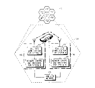
FIG. 1 is a diagram of a mobile subscriber unit 101
operating in a cellular radiotelephone system 100 having
5 two system providers (A 110 and B 112). The cellular
system 100 is designed to supply mobile telephone
service using a "cellular" radio coverage plan. This plan
divides a geographical area into a number of coverage
areas or "cells" 103-109 with each cell being assigned
10 to a portion of the available radio channels. The
channels used in one cell are again useable in spatially
separated cells in the same Mobile Service Area (MSA)
100.
Recommended minimum standards for the
15 subscriber unit 101 for use in the 800 MHz cellular
operating band may be found in the Cellular System
Mobile Station-Land Station Compatibility Specification
EIA-553 which assures that the subscriber unit 101 can
obtain service in any cellular system that meets the
20 compatibility requirements of EIA-553. Compatibility,
used in connection with EIA-553, is understood to mean
any subscriber unit 101 able to place and receive calls
in any cellular system, and all cellular systems are able
to place and receive calls with any subscriber unit 101.
25 To assure compatibility, it is essential that both radio-
system parameters and call-processing parameters be
specified. The sequence of call-processing steps that
the mobile and land stations execute to establish calls
has been specified in EIA-553 along with the digital
30 control messages and analog signals that are exchanged
between the system provider and the subscriber unit
101 .
The subscriber unit 101 communicates with a
distributed array of cell-site land stations, for example
20~0~68
,",, "
_ 7
111. The cell-site land station 111 is controlled by the
cellular-system network control and switching
equipment 11 3 that provides connection to the world-
wide telecommunications network 115. A call between
5 the land network 115 and a subscriber unit 101 is routed
via the cellular control system 1 13 to the cell-site 103
that best serves the location of the subscriber unit 101.
A call in progress can proceed indefinitely as the
subscriber unit moves from cell to cell throughout the
10 MSA 100 since it is automatically reassigned to an
available channel within a new cell.
Some of the channels within each cell are
dedicated to the control of the subscriber unit 101. This
includes locating a particular subscriber unit 101,
15 processing a subscriber-originated call, and performing
other system control functions. The remaining channels
are used for voice communication. The subscriber unit
101 gains access to the control channels by examining
the signal strength of each of a predetermined number of
20 potentially available channels and chooses the two
channels with the strongest signals. The subscriber unit
101 then tunes to the strongest control channel.
A subscriber unit is intended to be used while in
motion or during halts at unspecified points. It is
25 assumed that the subscriber unit 101 includes portable
units as well as units installed in vehicies. The basic
purpose of cellular telecommunications includes voice
and data communication.
FIG. 1 and the associated description provides the
30 setting for the solution provided by the present
invention. Simply stated, when the subscriber unit 101
is registered with System A and drives to a location in
the MSA 100, which is far from a System A cell-site
111 and close to a System B cell- site 117, the
2a~107 G8
, 8
,~
subscriber unit 101 produces IM distortion. The input
signal is characterized during the aforementioned
channel access routine to determine if the input signal
is from the subscriber unit's registered system or
5 generated intermodulation distortion caused by a strong
signal from the other system. The advantage offered by
the present invention, not found in the prior art, enables
a subscriber unit in a cellular system, specifically, to
drive near the transmitting site 1 17 of the other system
10 and maintain access to the far away transmitting site
111 of the system in which the subscriber unit is
reg i ste red .
The subscriber unit 101 required for a cellular
system is shown in FIG. 2 and consists of the following
units: a control unit 201, a transceiver unit 203
(including a. transmitter, a receiver and logic circuitry),
and an antenna unit 205. Although FIG. 2 depicts the
control unit 201, the transceiver unit 203 and the
antenna unit 205 as three separate units, all three may
20 be contained within a single housing if the physical
dimensions permit either mounting the combined unit
within reach of the vehicle operator, or using it as a
hand-held "portable" unit.
The control unit 201 is the interface between the
25 subscriber and the system. The subscriber interface
requirements may include a handset, a keypad, a loud
speaker, all subscriber-unit controls, indicators, and, if
provided, the digit display, with all of which the
subscriber interacts during the process of placing or
30 receiving a call. Portions of the control unit 201 may be
mounted in physically separate packages. A microphone
and loudspeaker combination or other peripherals may be
used in place of the handset to provide a means of using
the system without holding the handset.
2~76~
i,....
",~, g
The transceiver unit provides duplex voice
transmission and reception. The radio frequency (RF)
band is divided into two separate 25 MHz wide segments
each consisting of 832 channels. The first segment
5 from 824 to 829 MHz, contains the subscriber-unit
transmit channels. The second segment, from 869 to
894 MHz, contains the subscriber-unit receive channels.
Each subscriber-unit transmit channel is separated from
its duplex receive channel by 45 MHz.
The antenna unit 205 connects to the transceiver
unit 203 and consists of a vertically-polarized broad-
bandwidth antenna.
Now referring to FIG. 3, there is shown a receiver
portion of the transceiver unit 203 of FIG. 2. Received
15 signals at line 301, entering through the antenna unit
205 from the cell-site 111, arrive at the receiver where
they are amplified and demodulated. The signals may be
voice (which is passed to the control unit 201) or coded
signalling information (which is passed to the logic
20 circuitry 303 for decoding).
Examples of the coding orders received from a cell
site include orders to tune a transceiver to a new
frequency channel, to alert the subscriber to an
incoming call, to adjust the transceiver output power
25 and to release the subscriber unit upon completion of a
cal 1.
The input signal at line 301 is processed through a
broad band bandpass filter 305 that only allows
subscriber unit receive channels from 869 to 894 MHz to
30 be considered for demodulation by the receiver. System
A transmits signals from 869 to 880 MHz and from 890
to 891.5 MHz. System B transmits signals from 880 to
890 MHz and from 891.5 to 894 MHz. A filtered input
signal at line 307 is processed by an attenuator 309
20~076~
, ~,
1 0
,...~
having a predetermined magnitude of attenuation and
selectively coupled to a mixer 315 by a control signal at
line 311. In the preferred embodiment, the mixer 315 is
the nonlinear stage most likely to produce
5 intermodulation distortion in the receiver. With the
attenuator disabled, the filtered input signal at line 307
is coupled to the mixer 315 unattenuated. With the
attenuator enabled, the amplitude of the filtered input
signal signal is attenuated by the predetermined
10 magnitude before it is coupled to the mixer 315. The
mixer 315 converts the frequency of the filtered input
at line 313 signal to an intermediate frequency at line
319. Intermediate frequency block 317 processes the
intermediate frequency signal at 319 to generate a
15 received signal providing radio signal strength
indication (RSSI) at 321, provide selectivity for
adjacent and alternate channel interference protection
and processes the intermediate frequency signal into a
signal suitable for the audio band at 337. The received
20 signal providing RSSI at 321 is converted from an analog
to a digital signal at 323 wherein the digital signal at
325 is coupled to the audio and logic circuitry 303. The
logic circuitry measures the amplitude of the received
signal. In the preferred embodiment, a Motorola, Inc.
25 microprocessor MC68HC11E9 is used as part of the logic
circuitry and includes memory locations for storing
received data to be processed. Thus, the amplitude of
the input signal may be measured both attenuated and
unattenuated with the attenuator being switched in and
30 out, respectively. The audio signals at 337 processed by
the IF block 317 pass through the logic circuitry 303 to
the control unit 201 at lines 327. The logic circuitry
303 sends processed channel information to a frequency
synthesizer 329. The frequency synthesizer 329
2~768
"~.,
"~,
typically includes a crystal oscillator as a frequency
reference and a phase detector that, when combined
with the channel information and an output signal at line
335 from voltage controlled oscillator (VCO) 333,
5 generates a control voltage signal at line 331 to adjust
the frequency of the VCO 333. The VCO 333 supplies the
output signal at line 335 to the mixer 315 which
converts the RF signal at line 313 to the intermediate
frequency at line 319.
The apparatus of the present invention is not
intended to be limited to the specific receiver block
diagram of FIG. 3. The apparatus of the present invention
may be implemented with any receiver wherein the input
signal passes through the attenuator 309 before a
15 nonlinear receiving stage most likely to produce IM. The
measurement of the received signal strength occurs
after the nonlinear receiving stage most likely to
produce IM.
The apparatus and method of the present invention
20 is not limited to a receiver structure in which the
unattenuated and attenuated samples of the received
signal are taken at separate times. The present
invention may also be implemented utilizing a parallel
path receiver structure wherein the unattenuated and
25 attenuated samples of the input signal may be taken at
the same time. A parallel path receiver structure
comprises the block diagram of FIG. 3 with the
attenuator enabled so that an attenuated sample of the
input signal may be taken by the logic circuitry 303 in
30 addition to a second receiver path 345 having a mixer
339, intermediate frequency stage 341 and an A/D
converter 343 serially coupled together. The filtered
input signal at line 307 is coupled to the mixer 339
unattenuated. The mixer 339 utilizes the same signal
2~7076~
~,_ 12
335 from the VCO 333 as the other mixer 315. The
output from the A/D converter 343 is coupled to the
logic circuitry 303 at line 347. The audio signals at 351
processed by the IF block 341 pass through the logic
5 circuitry 303 to the control unit 201 at lines 327. The
second receiver path 345 is utilized to obtain an
unattenuated sampled of the input signal. Thus, a second
embodiment of the present invention utilizing two
receiver paths provides the opportunity to obtain
10 samples of the input signal's amplitude both attenuated
and unattenuated at the same time.
FIG. 3A is a block diagram of a portion of the logic
circuitry 303 illustrated in FIG. 3. The RSSI level of the
received signal generated by the intermediate frequency
15 block 317 is converted from a corresponding DC voltage
signal at line 321 to a digital signal at line 325 by the
A/D Convertor 323 and stored in a memory location of
the microprocessor 329. The input signal is attenuated
by switching in the attenuator 309 responsive to the
20 control signals at lines 311. The microprocessor 329 is
coupled to the flip flop 343 via four control lines at 341
(typically set, reset, data and clock). The flip flop may
be a conventional D-type flip flop having a part number
MC74HC74 and available from Motorola Inc.. The control
25 signals at lines 341 manipulate the control signals 311
of the flip flop in a conventional manner such that Q and
Q' are opposite logic levels (high and low). The RSSI
level of the attenuated received signal generated by the
intermediate frequency block 317 is converted to a
30 corresponding DC voltage signal and stored in another
memory location of the microprocessor 329. The RSSI
level of the attenuated received signal is subtracted
from the RSSI level of the unattenuated received signal
in a subtractor at block 331. The result of the
2~76~
..~.
13
subtractor 331 is a difference signal 343 that is
converted to an analog signal at block 333 and compared
to a reference signal at line 335 in a comparator 337.
The D/A convertor may be a quad six bit D/A having a
5 part number MC144111 and the comparator may be an
MC3302 quad comparator with an open collector output
both supplied by Motorola Inc.. The reference signal at
line 335 is determined by a variable resistor R4 biased
to a supply voltage, V. The reference signal at line 335
10 corresponds to at least one of the limits L1, L2 and L3
discussed with FlGs. 6A and 6B. The comparator 337
generates decision control signal 339 that has a logic
high or a logic low level, biased by a pull up resistor R5
to the supply voltage V, for the microprocessor 329. If
15 the decision control signal 339 is a logic high, the
received signal is determined to be a valid signal and
the input signal is processed. If the decision control
signal 339 is a logic low, the input signal is determined
not to be a valid signal and nontypical actions are taken
20 by the microprocessor 329. The nontypical actions will
be discussed with FlGs. 5 through 6B.
Now referring to FIG. 4, there is shown a detailed
circuit of the attenuator 309 coupled to a portion of the
logic circuitry 303 by line 311. The attenuator circuit
25 of FIG. 4 is shown as an example only. Other attenuator
circuits may be implemented in the apparatus of the
present invention. The attenuator 309 comprises a
conventional arrangement of resistors R1, R2 and R3,
capacitors C1, C2 and C3, and a PIN diode CR1. The
30 attenuator 309 is enabled when the logic circuitry 303
produces a logic high and logic low at outputs Q and Q,
respectively. With the attenuator enabled, the input
signal at line 307 is coupled to the mixer 315 at line
313 through DC blocking capacitor C1 and resistor R1.
' 2~7~76~
.......
14
......
The DC blocking capacitor C1 minimizes current drain in
the attenuator 309 when the attenuator 309 is
activated. Resistor R1 provides a series attenuation of
the received signal 307.
To disable the attenuator, a logic low and a logic
high signal is applied to Q' and Q, respectively, by the
logic circuitry 303. With the attenuator 309 disabled,
the PIN diode CR1 is forward biased effectively
becoming a short-circuit between the bandpass filter
305 and the mixer 315 allowing the input signal to pass
unattenuated. Resistors R2 and R3 provide DC current
limiting when the attenuator is disabled and minimizes
the RF signal loss between the bandpass filter 305 and
the mixer 315. By-pass capacitors C2 and C3 shunt
digital noise from the logic circuitry 303 to ground,
thus preventing corruption of the received signal at line
307. In the preferred embodiment, R1=220Q, R2=2.2KS2,
R3=2.2KQ and C1=C2=C3=33pF providing a typical
attenuation of 8 dB.
Now referring to FIG. 5, there is shown a novel
flow diagram describing a portion of the process of the
present invention carried out in the logic circuitry 303.
The flow diagram describes the novel process of
characterizing the input signal to determine if the
received signal is valid, invalid, or unsure. The signal
characterization is used to gain access to the system
service provider in which the radiotelephone is
registered without being distracted by strong signals
from the other system service provider. The logic
circuitry selects a channel at 501, then measures the
amplitude of the received signal S1 at 503 with the
attenuator 309 switched out. The measured amplitude
of received signal S1 is stored in a memory location at
504 in the logic circuitry 303. The attenuator 309 is
~ ~7 ~7 ~ ~3
. ,_
switched into the path of the received signal at 505 by
line 311 from the logic circuitry 303. The amplitude of
the attenuated received signal is measured at 507. The
measured amplitude of received signal strength S2 is
5 stored in a second memory location at 504 in the logic
circuitry 303. The attenuator is then switched out of
the path of the received signal at 509. To obtain the
best measurements the unattenuated and attenuated
received signals are taken within a predetermined time
10 period, such as less than one millisecond. The quick
sampling of the two signals will minimize the effects
of channel variation, due to fading for example, while
taking the two measurements. Thus, the logic circuitry
303 has acquired an unattenuated measurement S1 of
15 the receive signal strength and an attenuated
measurement S2 of the receive signal strength for a
given input signal.
The difference between the unattenuated signal
strength measurement and the attenuated signal
20 strength measurement S2 is determined at block 510.
The difference is compared to a predetermined limit at
block 511. The result of the comparison is processed at
513 to determine if the received signal corresponding to
a selected input signal is valid. A valid signal is an
25 input signal in which the measured difference between
the amplitude of the attenuated received signal and the
amplitude of the unattenuated received signal is
substantially equal to the predetermined magnitude of
the attenuator 309. If the received signal is valid, a
30 determination is made if it is one of the two strongest
received signals of all selected channels at 515. If the
valid signal is one of the two strongest, the strongest
signal list is updated with the valid signal at 525. The
- 2û~a768
~, ....
16
flow continues to block 519 to determine if all the
channels have been scanned.
If the received signal is determined not to be valid
at 513, the received signal is processed at 517 to
5 determine if it is invalid. An invalid signal is a received
signal in which the difference between the amplitude of
the attenuated input signal and the amplitude of the
unattenuated input signal is substantially equal to or
greater than three times the predetermined magnitude
10 of the attenuator 309 indicating that IM distortion is
present. If the received signal is not determined to be
invalid at 517 then it is unsure if the received signal is
valid or invalid. Therefore, the list of unsure input
signals at 523 is updated with the selected received
15 signal. The flow continues to block 519 to determine if
all the channels have been scanned. If the received
signal is determined to be invalid at 517 or if the input
signal is not determined to be one of the two strongest
at 515, a check is made to determine if all the channels
20 have been scanned at 519. If is determined that more
channels need to be scanned at 519, a new channel is
selected at 521 and the process of taking an attenuated
and unattenuated measurement of the received signal
corresponding to the selected input signal begins again
25 at block 503.
After all the channels have been scanned, the
decision flow continue to branch A in FIG. 5A. Branch A
uses only valid channels to decide how to process the
scanned channels. At decision branch A, the flow
30 continues to decision block 527 wherein a search is
made of the strongest signal list at 525. If no valid
signals were recorded, the channel scan begins anew at
501 represented by block 529. If valid signals were
recorded at 525, the valid signals are used in the normal
1 7 f~ O ~
receiving routine at 531 to gain access to the system
provider.
An alternate decision branch A in FIG. 5A is
decision branch A in FIG. 5B. Decision branch A in FIG. 5B
5 uses valid channels if they are available and unsure
channels if valid channels are not available. At decision
branch A, the flow continues to decision block 527
wherein the a search is made of the strongest signal list
at 525. If it is determined that valid signals were
10 recorded at 527, the valid signals are used in the normal
receiving routine at 531 to gain access to the system
provider. If no valid signals were recorded, a
determination is made at 535 if there are any signals
recorded in the unsure list at 523. If it is determined at
15 535 that no signals recorded in the unsure list at 523,
the channel scan begins anew at 501 represented by 529.
If it is determined at 535 that there are signals
recorded in the unsure list at 523, two of the strongest
unsure signals are selected from the list at 537. The
20 attenuator 309 is switched in at 539 and the two
strongest unsure signals are used in the normal
receiving routine at 531 to gain access to the system
provlder.
FlG's. 6A and 6B represent simple graphs forming
25 decision regions which are used to determine if the
received signal is valid, invalid or unsure. A valid
determination is represented in FIG. 5 as decision branch
514. An invalid determination is represented in FIG. 5 as
decision branch 518. An unsure determination is
30 represented in FIG. 5 as decision branch 520. The
horizontal axis 601 represents the measured difference
between the unattenuated amplitude of the received
signal, S1, and the attenuated amplitude of the received
signal, S2. FIG. 6A shows a predetermined limit L1
2070768
18
_
separating the measured difference values into two
decision regions. Predetermined limit L1 is
approximately half way along the expected range of
measured difference values on the horizontal axis 601.
5 If the measured difference is less than the
predetermined limit L1, the input signal is valid. If the
measured difference is greater than the predetermined
limit L1, the input signal is invalid.
FIG. 6B shows predetermined limits L2 and L3
10 dividing the measured difference values into three
decision regions: valid, unsure and invalid. If the
measured difference is less than the predetermined
limit L2, the received signal is valid. If the measured
difference is greater than the predetermined limit L3,
15 the input signal is invalid. If the measured difference is
between predetermined limits L2 and L3, the received
signal is in the unsure range.
Limits L1, L2, and L3 of FlGs. 6A and 6B are
presented as alternate examples of deciding what to do
20 with the attenuated and unattenuated signal strength
measurements. Other limits and decision regions may be
implemented inaccordance with the present invention to
detect IM distortion.