Note : Les descriptions sont présentées dans la langue officielle dans laquelle elles ont été soumises.
a o 7 3 2 8 0 PAT~NT
2088-33-00
PROCESS FOR AN IMPROVED LAMINATE OF ZnSe and ZnS
BACKGROUND OF THE INVENTION
This invention relates to a method for preparing an
infra-red transmissive window that is substantially free of
optical distortion. More particularly, it relates to a method
for preparing a laminate of zinc selenide and zinc sulfide
which overcomes the bimetallic effect arising from the
different coefficients of thermal e~rAncion of the two layers.
The IR window made by this invention meets the demands of
certain applications for which the prior art windows were
either unsuitable or prohibitively expensive.
An improved method for the chemical vapor deposition of
zinc sulfide on a zinc selenide substrate is taught in U.S.
Patent No. 4,978,577 of P.V. Purohit et al, issued December 18, 1990, and
assigned to CVD IncoIporated. There, the substrate is heated in the presence of
H2S and the absence of zinc vapor for a certain period of time
before the zinc vapor is introduced into the heating chamber.
The adhesion of the zinc sulfide to the substrate is greatly
improved by that tr~atm~nt. A problem inherent in the high
temperature lamination of materials having different
coefficients of thermal expansion is the bowing of the
laminate in response to the stress sometimes referred to as
"the bimetallic effect." The deposition of the zinc sulfide
occurs at a temperature of about 700~C. As the laminate is
cooled to room temperature, the initially flat upper
O 7 3~'~fl 0
PATENT
208~-33-00
surface of the zinc selenide substrate becomes convex and the
contiguous surface of the zinc sulfide is, perforce, concave.
If the substrate is mounted in the heating chamber in such a
way that it can not expand and contract freely, the bowing
will not be symmetrical and will be extremely difficult to
correct by optical grinding methods.
Infra-red transmissive windows made from such bowed
laminates are difficult to use in wide-angle "forward looking
infra-red imager" systems because of the optical path
differences (OPD) for the light rays that pass through the
window at different angles to the surface. As the angle of
incidence grows larger, the OPD becomes greater. An optician
can reduce the OPD by introducing some curvature into the
outer surfaces of the laminate to compensate for the
interfacial curvature. This is a lengthy and costly process,
especially when the curvature is unsymmetrical. Thus, the
bowing phenomenon is a deterrent to the widespread application
of the ZnSe/ZnS laminate as an infra-red window.
SU~ARY OF THE INVI~ N~1~1ON
It is an object of this invention, therefore, to provide
a method for the production of a zinc selenide/zinc sulfide
laminate having substantially no interfacial bowing.
It is a related ob~ect to provide a laminate of those
materials that needs no optical correction even though the
laminate was made by chemical vapor deposition of the sulfide
onto the selenide.
It is another related ob~ect to provide a "diffraction
limited" optical system comprising a chemical vapor deposition
laminate of zinc selenide and zinc sulfide.
These and othe- ob~ects of the invention which will
becoms apparsnt ~rom the following disclosure and the
accompanying drawings are achieved by establishing a heating
and cooling regimen for the chemical vapor deposition,
deterri ni ng the curvature of the interface between the
substrate and the deposit which will occur during the cooling
phase of said regimen, grinding the surface of the
znSe substrate to impart the negative of that
B
2~7328~
PATENT
2088-33-00
curvature to the surface of the substrate upon which the
zinc sulfide is to be deposited, heating the substrate
in a chemical vapor deposition chamber, coating that
surface with the sulfide by chemical vapor deposition,
and cooling the resulting laminate.
Another aspect of the invention is the provision of
a mounting frame which allows free lateral,
longitudinal, and transverse movement of the substrate
so that it may expand and contract freely during and
after the chemical vapor deposition of the zinc sulfide.
The amount and shape of the bowing that will occur
may be calculated using modern finite-element modelling
techniques since the mechanical and thermal properties
of ZnSe and ZnS are well known. The calculation of
stress induced by the bimetallic effect is taught by
Roark, Raymond J. and Young, Warren C., "Formulas for
Stress and Strain", 5th edn. McGraw-Hill, Inc., 1938,
Section 10-4, pp 337-381, "Bimetallic Circular Plates",
particularly in case 15a and also at page 366. The
bowing may also be measured by conventional optical
means, e.g., interferometry.
The present invention, therefore, in one aspect,
resides in an infra-red optical element comprising a
ZnSe substrate having a ZnS layer deposited on its
surface by chemical vapor deposition wherein the
interface is substantially planar.
The present invention further provides a laminated
structure comprising layers of ZnSe and ZnS which has
been heated to a temperature of about 700~C and has a
substantially planar interface between the layers.
The present invention, in another aspect, resides
in an improved method for the preparation of an infra-
red optical element by chemical vapor deposition of ZnS
B
~07~
3a PATENT
2088-33-oO
on a ZnSe substrate at high temperature which eliminates
the curvature of the interface caused by the unequal
coefficients of thermal expansion for the ZnS and ZnSe,
the improvement comprising:
establishing a heating and cooling regimen for the
chemical vapor deposition;
determining the curvature of the interface during
said regimen;
grinding the surface of the ZnSe substrate to
impart the negative of that curvature to the surface of
the substrate destined to be in contact with the ZnS;
and
coating the substrate with ZnS by chemical vapor
deposition;
whereby the interface between the ZnSe and ZnS is
substantially flat.
The present invention, in a further aspect, resides
in an improvement in a chemical vapor deposition
apparatus comprising a furnace, a mandrel box mounted
within the furnace and defining a vapor deposition zone,
the box comprising a mandrel plate having a passage
therein communicating with the vapor deposition zone, a
substrate holding frame removably mounted on said
mandrel plate in overlapping relation to the passage and
having an opening therein in alignment with said mandrel
plate passage, and a back plate removably mounted on the
holding frame plate as a closure for the opening, which
improvement comprises:
a restraint-free substrate holding frame and back
plate assembly having lips projecting toward each other
from opposite boundaries of the opening in the frame and
between the deposition zone and the back plate, the lips
adapted for support of a substrate to be placed in the
opening, the opening otherwise being larger than the
~ ~ 7 3 2 8 o
3b PATENT
2088-33-00
substrate to be placed in said opening, and the distance
between the lips and the back plate being larger than
the thickness of the substrate.
DESCRIPTION OF THE DRAWINGS
Turning now to the drawings:
FIG. 1 is a cross section of a laminate of the
prior art.
FIG. 2 is a graph of the coefficient of thermal
expansion of ZnSe and ZnS at increasing temperatures.
FIG. 3 is a cross section of a substrate mounted in
a frame inside a chemical vapor deposition furnace
according to this invention.
FIG. 4 is a cross-section of a broken away portion
of a hot vapor deposition furnace wherein ZnS is
deposited on the ZnSe substrate.
FIG. 5 is a sectional view taken along line 5-5 of
FIG. 4.
FIG. 6 is a graph of the sag of a ZnSe/ZnS laminate
of the prior art.
B
~ ~ 7 3 ~ 8 Q
PATENT
2088-33-00
FIG. 7 (located on the first sheet of drawings, with Figs. 1
and 2) is a cross section of the laminate of this invention after
deposition of the ZnS and cooling.
DETAILED DESCRIPTION OF THE lNv~NlloN
In FIG. 1, the ZnSe substrate 10 is bowed upward and is
seen to have a convex upper surface 12 and a concave lower
surface 14. The ZnS layer 16 is bowed in like manner. The
amount of sag is shown at 18 by the dimension lines depicting
the highest and lowest points of the curved surface.
The relation between the coefficient of thermal expansion
and the temperature for both the ZnSe and the ZnS is shown in
FIG. 2.
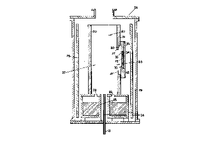
In FIG. 3 H2S is introduced into the mandrel box 20
through the pipe 21 to contact the ZnSe substrate 22 in the
absence of zinc vapor while the zinc metal 23 is being heated
in the pots 24,and when the zinc reaches its vaporization
temperature the vapor flows through the ports 26 into the
deposition zone 27. The mantrel box 20 is mounted upright in
the furnace 28 between the heating elements 29. The box is
made up of graphite plates, including the plates 30 and 31
shown here. The substrate holding frame 32 is mounted on the
mandrel plate 31 in defining relation to the passage 33
through the plate 31 to place the substrate within the passage
where it may be exposed to the vapors in the zone 27. As
shown in larger detail in FIGS. 4 and 5, the opening 34 in the
frame 32 is larger in each dimension than the substrate and
the distance between a lip 35 and the back plate 36 ~s greater
than the thickness of the substrate. A restraint-free
assembly is thus made a part of the furnace 28 so that the
bowing of the laminate upon cooling will be symmetrical and
can be remedied by the method of thi C in~Pntion . ~he lipe 35,
which project toward each other from opposite boundaries of
the opening 34 and are integral parts of the holding frame 32,
are adapted to the support of the substrate in an upright
position while blocking off only a minimal portion of the
passage 33 for vapors traveling toward the substrate.
8'7
PATENT
2088-33-00
In like manner, the shields 37 are integral parts of the
mandrel plate 31 which project toward each into the deposition
zone from opposite boundaries of the passage 33. They are
superposed over the outer periphery of the frame 32 to provide
a shadowing effect whereby the deposition of ZnS in the recess
38 of the mandrel plate and in the corners between the frame
and the plate is limited. The propagation of cracks from a
ZnS coating 40 on the mandrel plate 31 and the shield 37 into
the desired overcoat 39 on the substrate 22 is thereby
minimized by isolation of the overcoat from the deposits 40.
The amount and location of the bowing that would occur
during the deposition of ZnS onto a ZnSe substrate are shown
in FIG. 6. The substrate is 7.2 inches long, 5.5 inches wide,
and 0.70 inch thick; the thickne~s of the ZnS is to be 0.125
inch. Using the ANSYS~ finite element analysis program of
Swanson Analysis Systems,Inc. on an ARIES ConceptStation~
(Aries Technology,Inc.), the sag is calculated to be 78 ~m.
and symmetrical about the center of the laminate. From the
results of that calculation and in accordance with this
invention, a ZnSe substrate is ground and lapped to produce a
blank having a concave spherical surface with a total sag of
78 ~m. The blank is then mounted in the box 20 of FIG. 3 and
that assembly is placed in the vapor deposition zone 27 and
ZnS is deposited on the substrate at about 700~C as described
in U.S. Patent No. 4,978,577. Upon cooling to room
temperature, the laminate has a flat interface as shown at 41
in FIG. 7. The curvature that had been imparted to the
substrate mechanically is cancelled by the bimetallic effect
being put to work for us instead of against us.
PATENT
2088-33-00
The following computer program may also be used to calculate
the center sag of a laminate to be made by chemical vapor
deposition of ZnS on a ZnSe substrate:
30 REM: This is a program to calculate maximum deflection and
stress in a ZnS/ZnSe
40 REM: Window subjected to a change in temperature
50 REM: The equations used are from Roark
55 REM: ZnS is material 1, (top layer); ZnSe is material 2
(bottom layer)
60 REM: Following are the variables used
70 REM: A - radius of plate in inches
80 REM: Al - ther~Al eYpAn~ion coef. of material 1 in
inch/inch C
90 REM: A2 - Thermal exp~n~ion coef. of material 2 in
inch/inch C
100 REM: DT - Temperature gradient in degrees C
110 REM: Tl - Thickness of material 1 in inches
120 REM: T2 - Thickness of material 2 in inches
130 REM: El - Modulus of material 1 in psi
140 REM: E2 - Modulus of material 2 in psi
150 REM: KlP - Derived constant
160 REM: Vl - Poisson's ratio of material 1
170 REM: V2 - Poisson's ratio of material 2
180 REM: XYC - ToA~ng constant from Roark
310 LET Al=7.700001E-06
320 LET A2=8.300001E-06
330 INPUT "Temperature gradient"; DT
340 INPUT "Thickness of ZnS (material 1) in inches"; Tl
350 INPUT "Thickness of ZnSe (material 2) in inches"; T2
360 LET El=1.08E+07
370 LET E2=9750000
380 LET Vl=.29
390 LET V2=.28
"~ ~ 7
PATENT
2088-33-00
400 LET KYC=.5
410 LET KlP=4+(6*T1/T2)+(4*(Tl/T2) 2)+(El*T1 3*(1-V2))/
(E2*T2 3*(1-Vl))+(E2*T2*(1-Vl))/(El*Tl*(l-V2))
413 LET K2P=(l+((E2*T2 3*(1-Vl~2))/(El*Tl~3*(1-V2~2)))+
((3*(1-Vl~2)*(1+T2/Tl) 2*(1+(El*T1)/(E2*T2)))/
((l+El*T1/(E2*T2))~2-(Vl+(V2*El*T1)/(E2*T2))~2)))
416 LET K3P=(l+((V2*E2*T2 3*(1-V2~2))/(Vl*El*T1~3*(1-Vl~2)))+
((3*(1-Vl~2)*(1+T2/Tl)~2*(1+(V2*El*Tl/(Vl*T2*E2))))/
((l+(El*T1/E2*T2)))~2-(Vl+(V2*El*T1/(E2*T2)))~2)))
420 LET X = (6*(A2-Al)*DT*(Tl+T2))/(KlP*T2~2)
425 INPUT "Enter plate radius in inches"; A
427 REM: Calculate center deflection
430 LET Y = KYC*X*A~2
500 PRINT
510 PRINT
520 PRINT "ZnSe Thickness";T2;" inches","ZnS thickness";Tl;"
inches"
521 PRINT
522 PRINT "Plate ~adius";A;" inches","temperature gradient";
DT;" degrees C"
523 PRINT
530 PRINT "The maximum deflection is ";Y;" inches"
532 REM: Calculate stresses associated with deflection
535 LET VE = Vl*(K3P/K2P)
540 LET DE = (El*K2P*T1 3)/(1-Vl~2))
545 LET L8 = .5*(1+VE)
550 LET M = DE*X*(1-VE)*(l-L8)
560 LET Sl = ((-1)*6*M/(T1 2*K2P))*(l+(((l-V1 2)*(1+T2/T1)*
(l+(El*Tl/(E2*T2)))) ((l+(El*Tl/(E2*T2)))~2-
(Vl+(V2*El*Tl)/(E2*T2)))~2)))-((A2-A1)
*DT*E1/((1-Vl)*KlP*(3*Tl/T2+2~(Tl/T2~~2
((E2*T2~(1-Vl))/(El*T1*(1-V2)))))
563 LET S2A = E2*T2*(1-V1 2)/(El*Tl*(l-V2 2))
565 LET S2N = (l-Vl 2)*(1+T2/Tl)*(l+El*Tl/(E2*T2))
567 LET S2D = (l+El*Tl/(E2*T2))~2-(vl+v2*El*Tl/(E2*T2))~2
PATENT
2088-33-00
568 LET S2S = ((A2-Al)*DT*E2)/((1-V2)*KlP)*(3*tTl/T2)+2-
((El*T1~3*(1-V2))/(E2*T2~3*(1-V1))))
570 LET S2 = (6*M/(Tl~2*K2P))*(S2A+(Tl/T2)*S2N/S2D)+S2S
575 PRINT
576 PRINT
580 PRINT "The stress of top surface of ZnS is "jSl;"PSI"
590 PRINT "The stress on bottom surface of SnSe is ";S2;"PSI"
750 END
NOTE: An asterisk is a multiplication sign here; indicates
superscript follows
-- 8
- 2~Y3 2~ 0
PATENT
2088-33-00
A particular example of the process of this invention i8
as follows:
The potential center sag of the interface of a laminate
window measuring 11.75 X 7.25 inches and having a ZnSe
thickness of 0.72 inch and a ZnS thic~ness of 0.06 inch wa~
calculated, using the above program, to be 22.9 ~m over a 6
inch chord spanning the bowed interface. A ZnSe substrate
having the recited dimensions was then fabricated to have a
concave surface with a radius of curvature equal to -5000 +
500 inches and the calculated center sag on one side. The
substrate was loaded into the restraint-free holding frame 32
and the assembly was mounted over the passage 33 of the plate
31 so that the concave surface would be exposed to the zinc
and H2S vapors in the zone 27. After the su~strate was coated
with the ZnS to the desired thickness of 0.06 inch and the
laminate was cooled, the window was ground flat on the top and
bottom surfaces to the proper thicknesses. The radius of
curvature of the interface was measured as -347,640 inches and
the center sag was -0.3 ~m over the 6 inch span. Thus, the
bowing of the interface was reduced more than 98 %.
The method of this invention places no limits on the
dimensions of the window that may be produced -- one
measuring 18 X 12 inches having been fabricated by it -- but
as a practical matter the larger the window the thicker it
must be for rigidity. Because its transmission in the
infra-red is poorer than that of the ZnSe, the thickness of
the ZnS layer on the final window should be no greater than
what is required for its function as a protector of the
substrate against erosion by rain and dust particles at high
speeds. The minimal thickness for that protection is about
0.030 inch. The actual thi-~ness deposited, however, will be
considerably srea.~r, i.e., about 0.10 inch, to allow for the
optical grinding and polishing that is necessary to provide
the desired window.
The window prepared by the method of this invention is
essentially "diffraction limited", the optimal condition when
PATENT
2088-33-00
one is considering the distortion of an image by an optical
system. The transmitted wave front aberration for rays that
are not normal to the surface of the window prepared according
to this invention is less than 0.1 of a wavelength for rays
40-60~ from normal. In contrast, the window having the curved
interface caused by the bimetallic effect gave aberrations in
the range of 0.3-0.7 wavelength in the infra-red (i.e., one
wavelength = 10.6~m).
-- 10 --