Note : Les descriptions sont présentées dans la langue officielle dans laquelle elles ont été soumises.
2~4~
DIGITAL MODULATORS FOR USE WITH SU~-NYQUIST SAMPLING
OF RASTER-SCANNED SAMPLES OF IMAGE INTENSITY
The invention pertains to digital synchronous modulators and,
5 more particularly, to such modulators operated for sub-Nyquist
sampling digital video signals descriptive of raster-scanned
samples of image intensity, thereby to generate folded video signals
of reduced bandwidth.
Back~round of the InventlQ~
Television systerns have been proposed which use sub-Nyquist
sampling of the luminance signal for obtaining increased resolution
through frequency interleaving, while keeping the frequency
spectrum occupied by the luminance information the same, and for
achieving at the same time some degree of backward compatibility
with existing television receivers. In sub-Nyquist sampling of a
progressively scanned television signal, in a first set of alternate
frames every odd sample in odd-numbered lines is replaced by a zero
and every even sample in even-numbered lines is replaced by a zero,
in a second set of alternate frames (interleaved in time with the
first set) every even sample in odd-numbered lines is replaced by a
zero and every odd sample in even-numbered lines is replaced by a
zerol and the zero samples are not transmitted. Fielci-interlaced
television signals can also be sub-Nyquist sampled. The sub-Nyquist
sampling of a luminance signal of up to twice the bandwidth of a
conventional broadcast luminance signal generates a "foldeci-
luminance~ signal with a bandwidth no more than that of a
conventional broadcast luminance signal.
E. A. Howson and D. A. Bell describe frequency interleaving of
luminance information in the analog domain in an article "Reduction
of Television Bandwidth By Frequency Interlace" in pages 127-136
of the February 1960 Journal of the Briti~h Institute of Radio
Enç~ineers. In one seheme envisioned by Howson et alii the entire
luminance signal is used to ampiitude-modulate a carrier having a
freciuency just above the highest frequencies in the luminance
, :
2 2~7~9~
slynal, and the resulting signal is supplied to a low-pass filter
having a cut-off frequency at mic~-band. In another scheme
envisioned by Howson et alii the luminance signal is separated by a
band-splitting filter into two components residing in respective
5 ones of equal-bandwidth low-frequency and high-frequency bands,
the high-frequency-band component is used to amplitude-modulate a
carrier having a frequency just above the high-frequency band, and
the lower sideband resulting from the amplitude modulation is
combined with the low-frequency-band component to obtain a
10 folded-luminance signal. Reducing television bandwidth by
frequency interlace cannot be satisfactorily implemented in the
analog domain, however, because of the difficulty of removing
artifacts introduced by the frequency interleaving that manifest
themselves as annoying dot crawl in the reconstructed full-band
15 television image.
There have been proposals to use sub-Nyquist sampling of the
luminance signal to improve home video cassette recorders (VCRs)
using the VHS format. The VHS format is a color-under format. The
chrominance information is recorded as in-phase and quadrature
20 amplitude-modulated sidebands of a suppressed 629 kHz carrier,
which is the fortieth harmonic of horizontal synchronization rate.
The luminance information is recorded as frequency modulation of a
carrier which can vary in frequency from 3.4 to 4.4 MHz (+ or- 0.1
MHz), to occupy a 1.4 - 7.0 Mhz band after filtering to suppress
25 sideband energy below 1.4 MHz. The luminance and chrominance
carriers are recorded and played back using helically scanning heads
mounted in a rotating headwheel assembly, with these two
components of video information being recorded on diagonal tracks.
Stationary heads can be used for recording and playing back sound
30 in~ormation recorded in lateral sound tracks on the video tapes.
Alternativeiy, high-fidelity stereophonic sound can be recorded on
and played back from deep diagonally recorded sound tracks by
helical scanning procedures implemented by wide-gap heads also
included in the rotating headwheel assembly. The high-fidelity
35 stereophonic sound frequency-modulates a 1.2 MHz carrier.
, .
2~7~96
One such modification of VHS format video tape recording was
proposed by Faroudja in U. S. patent No. 4,831,463 issued 16 May
1989 and entitled "VIDEO PROCESSlt`lG IN WHICH HIGH FREQUENCY
LUMINANCE GOMPONENTS ARE FOLDED INTO A MI~BAND SPECTRUMn.
In the Faroudja video recording system (according to column 9, lines
30-35, of U. S. patent No. 4,831,463) the sub-Nyquist folding
frequency is carefully chosen from amongst those frequencies which
are precise harmonics of an odd multiple of both the line and frame
scan rates of the baseband luminance. Faroudja performs sub-
Nyquist sampling on the entire luminance signal, sampling at a
folding clock frequency rate to generate a reversed frequency
spectrum frequency-translated to baseband, there to interleave with
the original frequency spectrum, and then applies the result to a
low-pass filter cutting off at one-half the folding clock frequency
to generate the folded-luminance signal. This procedure amplitude-
modulates the folding clock frequency in a modulation procedure
that -- though it may be balance~ with regard to suppressing the
folding clock frequency -- cannot be balanced with regard to
modulating signai.
Another modification of VHS format video tape recording was
briefly described by C. H. Strolle, J. W. Ko and Y. J. Kim in their paper
"A Compatibly Improved VHS System" appearing on pages 122-123 of
IEEE 1991 International Conference on Consumer
Electronics Digest of Technical Papers for a conference held
5-7 June 1991 in Rosernont, Illinois. This improved VHS video
recording system is described in more detail in the U. S. patent
application serial No. 787,690 filed by Christopher H. Strolle et alii,
entitled "SYSTEM FOR RECORDING AND REPRODUCING A WIDE
BANDWIDTH VIDEO S1GNAL VIA A NARROW BANDWIDTH MEDIUM" and
assigned to Samsung Electronics. In this improved video recording
system the sub-Nyquist folding carrier is chosen to be 320 times
line scan rate, rather than one of the frequencies specified by
Faroudja in U. S. patent No. 4,831,463.
To avoid generatin0 aliasing artifacts that are intolerabie to a
person viewing a television image recovered from the video signal
sampled at sub-Nyquist rate, before recording the luminance signal,
2 ~ 7 ~
the video recording system described in U. S. patent application
serial No. 787,690 processes luminance as described immediately
hereinafter. A band-splitting filter is used to separate a spatio-
temporally filtered luminance signal into low-frequency-band and
5 high-frequency-band spectra. The high-frequency-band spectrum is
adaptively de-emphasized, or reduced in amplitude respective to the
low-frequency-band spectrum.
If after its de-emphasis the high-frequency-band spectrum
were re-combined with the low-frequency-band spectrum to
10 generate a full-band luminance signal with de-emphasized high
frequency content, the generation of folded-luminance signal from
that full-band signal by the method Faroudja uses introduces a
problem during playback with regard to restoring the de-emphasized
high-frequency-band spectrum to its original amplitude respective
15 to the low-frequency-band spectrum. This problem arises because,
in addition to the roll-off of the lower frequencies of the high-
frequency-band spectrum caused by the band-splitting filter used to
separate the spatio-temporally filtered luminance signal into low-
frequency-band and high-frequency-band spectra, there is an
2 0 additional roll-off of the lower frequencies of the high-frequency-
band spectrum caused by the low-pass filter used in generating the
folded-luminance signal from the sub-Nyquist-sampled full-band
sig nal .
This additional roll-off is avoided in the video recording
25 system described in U. S. patent application serial No. 787,690 by
applying the de-emphasized high-frequency-band spectrum to a
balanced modulator, wherein that modulating signal is heterodyned
with the folding carrier. The modulation procedure is one that
suppresses modulating signai as well as folding clock frequency in
30 the modulation result. The resulting balanced modulator output
signal is a reversed spectrum frequency-translated to baseband and
unaccompanied by the original spectrum of the modulating signai
This reversed spectrum, which encodes the de-emphasized high-
frequency-band spectrum, has only the roll-off of the original band-
3 5 splittin~ fiiter. There is an absence of significant spectral energyin the frequency range below the folding clock frequency occupied by
5 2074~
the original de-emphasized high-frequency-band spectrum or in the
mirrored frequency range above the folding clock frequency Above
the folding clock frequency there is also an absence of significant
spec~ral energy in the mirror of that frequency range. That is, the
balanced modulator output signal is free of first-harmonic (and all
other odd-harmonic) sidebands of the folding clock frequency. The
balanced modulator output signal i~ added to the low-frequency-
band spectrum to generate a folded-luminance signal. It is then easy
for one skilled in the art of filter design to design a low-pass filter
for suppressing the even-harmonic sidebands of the folding clock
frequency generated by the balanced modulator, while not
introducing objectionable additional roll-off of the folded-
luminance signal near the cross-over frequency of the band-splitting
filter.
The folded-luminance signal is supplied as a modulating signal
to a frequency modulator. A frequency-modulated luminance carrier
generated by the frequency modulator is combined with a complex-
amplitude-modulation color-under carrier to generate a recording
signal for the helically scanning video record head(s).
During playback the video recording system described in U. S.
patent application serial No. 787,690 operates in the following
manner. The frequency-modulated luminance carrier and the
complex-amplitude-modulation color-under carrier in the playback
signal recovered by the helically scanning video playback head(s) are
separated from each other by respective band filters before each is
demodulated. The folded-luminance signal is recovered by detecting
the frequency modulation of the luminance carrier and then
subjecting the detected folded-luminance signal to an unfolding
procedure. In this procedure the folded-luminance signal is supplied
as a modulating signal to a modulator, to be heterodyned with the
folding carrier to restore its reversed spectrum portion to its
original high-frequency band. This heterodyning procedure generates
an undesirable image of the low-frequency band accompanying the
high-frequency band in its portion of the spectrum. The low-
frequency band, the restored high-frequency band and the high-
fre~uency-band image of the low-frequency band ar0 spatio-
6 2~7~
temporally filtered to suppress the image, thus to recover the
luminance signal with a de-emphasized high-frequency-band
The de-emphasized high-frequency-band spectrum is separated
from the low-frequency band by a band-splitting filter and re-
5 emphasized to restore its original amplitude vis-a-vis the
amplitude of the original baseband spectrum. It is this restoration
step that would be hampered by roll-off of the lower frequencies of
the high-frequency-band spectrum that is additional to that
associated with the band-splitting filter used during recording.
10 Such roll-off would tend to introduce a reduction in the amplitude of
of mid-spectrum frequencies~
The amplitude-restored high-frequency-band spectrum is then
rejoined with the low-frequency band from which it was separated,
thereby to recover a full-bandwidth replica of the wide-bandwidth
15 luminance signal. This wide-bandwidth luminance signal, the
chrominance signals demodulated from the complex-amplitude-
modulation color-under carrier, and the sound signal recovered from
the audio tape track are suitable for being encoded in substantial
accordance with a broadcast color television standard and used to
20 amplitude-modulate a broadcast-band carrier wave, thereby to
generate signals suitable for application as input signals to a color
television broadcast receiver. Alternatively, this wide-bandwidth
luminance signal, the chrominance signals, and the sound signal may
be supplied directly to a color television monitor, rather than being
25 used to amplitude-modulate a broadcast-band carrier wave.
The generation of the folded video signal proceeding from a
wide-bandwidth luminance signal and the regeneration of the wide-
bandwidth iuminance signal proceeding from the folded video signal
are procedures best carried out in the digitai, rather than analog,
30 regime. Generally, a balanced modulator is realized in the digital
regime as follows. A pair of four-quadrant digital multipliers are
used for multiplying samples of a digitized modulating signal by
samples of a first digitized carrier wave and by samples of a second
digitized carrier wave opposite in phase to th~ first, and a digital
35 adder combines the two digital products that result to generate the
output signal of the balanced modulator. Digital multipliers that
'
7 2~7~
operate at video sample rates are expensive, taking up large areas on
a monolithic integrated circuit. Such multipliers consume
substantial power and so present problems with ge~ting rid of the
heat they generate.
Choosing the luminance sampling rate to be twice the folding
carrier frequency in a folded-luminance signal employed in a video
recording system causes the lower of the first-harmonic sidebands
of the sampling frequency to fall into a frequency range immediately
above the baseband spectrum. This would appear to interfere with
the folding of the luminance spectrum. The high-luminance-
frequency spectra in the baseband and in the lower first-harmonic
sideband combine, however, to provide a frequency spectrum that is
the equivalent of a band-pass filter response centered at the folding
carrier frequency. A balanced modulator operated at folding carrier
frequency responds to the band-pass filter response centered at the
folding carrier frequency to generate an output signal in which the
two high-luminance-frequency spectra fold together around zero
frequency to form a reversed high-luminance-frequency spectrum,
without the expected interference arisin~. Choosing the luminance
sampling rate to be twic~ the folding carrier frequency in a folded-
luminance signal employed in a video recording system reduces
balanced modulation of a suitably phased folding carrier wave to
multiplication of successive samples of the modulating signal
alternately by plus one and by minus one. Such multiplications are
~5 done without having to use a digital multiplier.
~ummary Qf the Invention
Video signal, which is a baseband signal of a prescribed
bandwidth extending up to a prescribed maximum frequency, is
processed by apparatus embodying the invention to generate a
folded-spectrum video signal. The video signal is digitized and
supplied to a digital band-splitting filter with a cross-over
frequency at one-half said prescribed maximum frequency, for
3 5 separating the digitized video signal into samples of a lower-
frequency-band component and into samples of a hi~her-frequency-
8 ~7~9~
band component. A balanced modulator is connected for modulating a
folding carrier wave of the prescribed rnaximum frequency, which
modulation is done in accordance with ~he higher-frequency-band
component to generate a balanced modulation signal; and the
5 balanced modulation signal is linearly combined with the lower-
frequency-band component to generate the folded-spectrum video
signal. In apparatus embodying the invention in a preferred form,
the sampling rate of the digitized video signal is exactly the Nyquist
rate of the prescribed maximum frequency, reduces the balanced
10 modulation of a suitably phased folding carrier wave to
multiplication of successiYe samples of the modulating signal
alternately by plus one and by minus one. Such multiplications are
done without having to use a digital multiplier.
Brief D~criptioQ of the Drawin~
FIGUR~ 1 is a schematic diagram of video tape recorder
electronics for phase-locking to horizontal sync the sampling of
luminance signal (and of 3.58 MHz chrominance sidebands, during
2 0 recording), which electronics includes circuitry providing sub-pixel
phasing control (SPPC) during playback.
FIGURE 2 is a schematic diagram of video tape recorder
electronics for identifying the scan lines into which a sub-pixel
phase reference signal is inserted during recording to implement
2 5 sub-pixel phasing control during playback, which electronics
includes a counter for generating modulo-two counts of the fields
and frames of video signal.
FIGURE 3 is a schematic diagram of video tape recorder
recording electronics used for separating digitized composite video
3 0 signal into luminance, chrominance and motion signal components.
FIGURE 4 is a schematic diagram of video tape recorder
recording electronics used for generating folded-luminance signals
in which components in a higher-frequency (e. g., above 2.5 MHz) band
have been de-emphasized, which electronics includes a baianced
35 modulator and embodies the invention.
- .~ . '
2~7~9g
FIGURE 5 is a schematic diagram of video tape recorder
playback electronics used for unfolding the folded-luminance signal,
for separating the motion and chrominance signals from the color-
under carrier, and for remodulating the chrominance sidebands back
5 onto a suppressed 3.58 MHz color subcarrier.
FIGURE 6 is a diagram of the kernel of weights used in the
quadrant-selective filter of FIGURE 5.
FIGURE 7 is a schematic diagram of video tape recorder
playback electronics that process the unfolded luminance signal to
10 undo the de-emphasis of components in a higher-frequency (e. g.,
above 2.5 MHz) band done in the recording procedure, that combine
the resulting luminance signal with the chrominance sklebands
remodulated back onto a suppressed 3.58 MHz color subcarrier in
FIGURE 5 circuitry and thus generate a composite video signal, and
15 that modulate a television band radio-frequency carrier with the
composite video signal and a sound subcarrier in substantial
accordance with NTSC standards.
FIGURE 8 is a schematic diagram of a sub-pixel phase
reference generator, constructed as a state machine and suited for
20 inclusion in the FIGURE 1 video tape recorder electronics.
FiGURE 9 is a schematic diagram of sub-pixel phase control
circuitry, suitable for inclusion in the FiGURE 1 video tape recorder
electronics.
FiGURE 10 is a schematic diagram of one forrn of correlation
25 filter that can be used in the FIGURE 9 sub-pixel phase controi
circuitry.
FIGURES 11-18 show various alternative forms of balanced
modulator that can replace that specifically shown in FIGURE 4.
FIGURES 19-24 comprise a set of frequency spectra sharing
30 the same axis of abscissas in frequency, which spectra are
descriptive o~ video tape recorder e!ectronics using folded
luminance signals in which digitization is carried out at a rate three
times the folding carrier frequency.
FIGURES 25-30 comprise a set of frequency spectra sharing
35 tho same axis of abscissas in frequency, which spectra are
descriptive of video tape recorder electronics using folded
1 o 2 ~ J ~i
luminance signals in which digitization is carried out at a rate three
times the folding carrier frequency.
FIGURES 31-36 comprise a set of frequency spectra sharing
the same axis of abscissas in frequency, which spectra are
5 descriptive of video tape recorder electronics using folded
luminance signals in which digitization is carried out at a rate three
times the folding carrier frequency.
The axes of abscissas in frequency for FIGURES 19-36 are
calibrated in megahertz (MHz).
In the figures of the drawing and in the detailed description of
those figures which follows this paragraph, the depiction and
description of equalizing delays are usually omitted for the sake of
emphasizing the distinctive features of the invention and avoiding
losing sight of those distinctive features among a crowd of
conventional details generally found in video recording systems. One
skilled in the art of designing such systems will appreciate the need
for such delays to properly align video signals respective to each
other and to compensate for unwanted differential delay between
video signals arising from differences in the way these signals are
processed. Such a skilled person will understand where those delays
are necessary and what their values must be.
Further, where analog-to-digital converters are shown or
described, one skilled in the art will understand the desirability of
preceding them with analog low-pass filters for anti-aliasing; and
where digital-to-analog converters are shown or described, one
skilled in the art will understand the desirability of following them
with analog low-pass filters for suppressing clocking remnants and
quantizing noise. These filters will not be explicitly shown nor
hereafter described.
3 0 In block schematic diagrams control signal connections are
shown in dashed line and data signal connections are shown in solid
line.
Qetal!e~ Des~rJ~iQn
. .: .
2~7~
1 1
The invention will be described in the context of a video tape
machine with both tape recording and tape playback capabilities,
although the invention may be embodied in certain of its aspects in a
video tape machine with but one of these capabilities. The invention
does not concern the way in which the sound accompanying the video
is recorded and played back. So, for the sake of simplicity in the
following description, the apparatus associated with the recording
and playing back of the sound accompanying the video, which is
conventional in nature, is not described. In a video tape machine
10 with both tape recording and tape playback capabilities, it is
commonplace to use portions of the electronics both during
recording mode and during playback mode and to reconnect those
portions in different ways in the two modes, using a multiple-pole
record/playback switch. The elements in those portions of the
15 electronics used both during recording mode and during playback
mode will be identified by the same numbers when describing either
mode of operation; and the details of the multiple-pole
record/playback switch connections of these elements will not be
specifically descri~ed, inasmuch as the understanding of the details
20 of these interconnections is elementary to engineers of ordinary
skill in the art of designing recording and playback electronics for
video tape machines. The multiple-pole record/playback switch can
be entirely mechanical in nature, being provided by a wafer switch,
for example; or the switch may be realized in whole or in part by
2 ~ electronic means.
Referring to FIGUR~ 1, an ANALOG VIDEO signal is selected by
a pole 2 of a record/playback switch from a source 3 of NTS~ signal
during recording or ~rom a playback amplifier 4 durin~ playback. The
source 3 of NTSC signal may be a video camera or a television
30 receiver front end. During playback, the playback amplifier 4 is
connected by another pole 5 of the record/playback switch to the
helically scanning tape heads 6 of the video tape transport.
The C:OMPOSITE VID~O signal is applied to an analog-to-
digital converter 7 for digitization, to a horizontal sync separator 8
3 5 that separates horizontal synchronizing pulses to generate a
HORIZONTAL SYNC signal, and to a vertical sync separator 9 that
1 2 2~7 ~9 ~
s~,~arates vertical synchronizing pulses to generate a VERTIC~AL
SYNC signal. During playback from a video tape recording, the
COMPOSITE VIDEO signal is obtained from the helically-scanning
playback head(s) of the video tape transport. During video racording
5 the COMPOSITE YIDEO signal may be supplied from a video camera,
from a video tape player playing another video tape recording, or
from the video (or "second") detector of a television receiver.
A frequency-and-phase-controlled master oscillator 10
generates master clocking pulses at a rate 640 times horizontal
10 synchronizing pulse rate, as controlled by an automatic-frequency-
and-phase-control (AFPC) loop locking to the HORIZONTAL SYNC
signal from the horizontal sync separator 8. The horizontal sync
separator 8 is preferably of a type in which the equalizing pulses do
not accompany the separated horizontal sync pulses in the
15 HORIZONTAL SYNC signal. AFPC loop errors that mistime the
horizontal scan lines occuring just after the vertical retrace
interval are avoided by eliminating the equalizing pulses in the
horizontal sync separator 8 output signal HORI~ONTAL SYNC. The
equalizing pulses can be eliminated responsive to vertical retrace
20 blanking supplied to the horizontal sync separator 8 from the
vertical sync separator 9 via the control signal connection shown in
FIGURE 1 when the AFPC loop is in lock. It is also possible to use
the short-pulse eliminator well-known in RADAR to eliminate
equalizing pulses in the HORIZONTAL SYNC signal. The AFPC loop
2 5 controlling oscillator 10, which loop uses a pulse discriminator
keyed by separated horizontal sync pulses for generating locking
signals, will now be described.
The master clocking pulses are applied to the carry-in
terminal of a nine-stage binary counter 11 supplying its count
30 output to a decoder 12, which detects when a three-hundred-
nineteen binary count is reached to reset the counter 11 to zero
next count. The counter 11 accordingly generates a l\llOl)ULO-320
PIXEL COUNT signal, repeatedly counting the number of luminance
samples in one half a scan line to generate digitized sawteeth at
3 5 twice scan line rate.
, ' .
~` :
1 3 2 ~ 6
The MODULO-320 PIXEL ~::OUNT signal addresses a read-only
memory (ROM) 13 that stores a discriminator characteristic that is
zero-valued at zero count, that is substantially symmetric about
zero count, that exhibits a high slope through zero count, tha~ is
5 flattened for a wide range of counts from a few counts above zero to
one-hundred-fifty-nine binary count, and that is also flattened for a
wide range of counts from one-hundred-sixty binary count to a few
counts below three-hundred-nineteen binary count. The high slope of
the discriminator characteristic through zero count is used to
10 improve the tightness of phase lock in the AFPC loop. Two complete
discriminator characteristics are swept through in each of
consecutive intervals, each of the same time duration as a
horizontal scan line. One of these discriminator characteristics is
used to maintain lock to horizontal sync pulses in odd fields of scan;
15 and the other of these discriminator characteristics is used to
maintain lock to horizontal sync pulses in even fields o~ scan,
refective of the half-scan-line offset between horizontal sync
pulses in the two fields. Responsive to each horizontal sync pulse
from the horizontal sync separator 8, a keyed latch 14 latches the
2 0 concurring in time value of the discriminator characteristic read
from the ROM ~3, the latched value to serve as the digitized error
signal for the AFPC loop. This digitized error signal is converted to
an analog error signal by a digital-to-analog converter 1~. The
analog error signal is supplied to the loop filter 16, the response of
25 which is applied as AFPC signal to the controlled master clocking
oscillator 1 0.
The eight least significant bits of the l\llODIJLO-32~ PIXE~
COU~IT signal addresses a read-only memory (ROM) 17 that stores
sine and cosine tables for generating a four-phase 4.21 MHz sarrier
30 wave. The four least significant bits of the MODULO 3~0 PIXEL
{:OUNT signal addresses a read-only memory (ROM) 18 that stores
sine and cosine tabl~s for generating an unmodulated four-phase 629
kHz color-under carrier wave.
FIGURE 1 also shows sub-pixel phase control circuitry now to
35 be described. The master clocking pulses supplied from controlled
oscillator 10 at 640 times horizontal synchronizing pulse rate are
14 2~7~9~
applied as input signal to a tapped analog delay line 19, the signals
at the successive taps of which are delayed by successive sub-pixel
increments. Responsive to a command supplied by sub-pixel phase
control circuitry 20, a multiplexer 21 selects one of these subpixel
5 phases of the master clocking pulses for application as a sampling
command to the analog-to-digital converter 7. During recording, a
prescribed median subpixel phasing is imposed by the control
circuitry 20.
During recording only, a luminance-phase-lock key generator
10 22 generates a RECORD LUMA-PHASE~LOCK KEY or R L-P-L KEY
signal that goes to logic ONE during that portion of a scan line that
occurs during or immediately after vertical retrace interval, into
which line portion the signal for controlling sub-pixel phase is
inserted. The R L-P-L KEY signal is used for controlling a
15 multiplexer 23 that selects, as a DIGITAL VIDEO signal, the output
signal from a sub-pixel phase reference signal generator 24 when
the R L-P-L KEY signal is ONE, or the digitized COMPOSiTE VIDEO
signal from converter 7 when the R L-P-L KEY signal is ZERO. The
sub-pixel phase reference signal generator 24 receives control
20 signals from the luminance-phase-lock key generator 22.
During play-back, the luminance-phase-lock key generator 22
generates a PLAYBACK LUMA-PHASE-LOCK KEY or P-E3 L-P~L
KEY signal that goes to logic ONE during that portion of a scan line
that occurs during or immediately after vertical retrace interval,
2 5 into which line portion is inserted the signal for controlling sub-
pixel phase. The sub-pixel phase control circuitry 20 responds to
the P-E~ L-P-L KEY signal going to ONE to adjust the sub-pixel
phasing in accordance with the signal for controlling sub-pixel
phase contained in the COMPOSITE VIDEO signal recovered durin~
30 playback from the video tape recording and digitized by the analog-
to-digital converter 7.
FIGURE 2 shows particulars of the luminance-phase-lock key
generator 22 of FIGURE 1. A ten-stage binary counter 25 in FIGURE
2 counts the pulses from the decoder 12 that in FIGURE 1 resets the
35 counter 11 used to generate MODllLO-320 PIXEL COUNT. These
pulses occur at twice scan line rate, so the count output signal from
'
1 5 207~9~
the counter 25 is a HALF-LINE C~JNT signal. In FIGURE 2 a
decoder 26 resets the count from the counter 25 to zero after a
count of fiYe-hundred-twenty-four, so counter ~5 counts half scan
lines over a field. The resetting signal, generated by decoder 26
5 output signal going high responsive to a count of five-hundred-
twenty-four, is applied to the counter 25 via an OR gate 27.
The OR gate 27 receives from an AND gate 28 another reset
signal for application to the counter 25 when it is determined there
is a vertical synchronization error in the counter 25 half-line count,
10 with regard to the separated vertical sync pulses supplied from the
vertical sync separator 9 of FIGURE 1. The AND gate 28 receives
these separated vertical sync pulses as one of its input signals, the
other of its input signals being a logic ONE only when it is
determined there is a vertical synchronization error in the HALF-
15 LINE COUNT from the counter 25. At such time the AND gate ?8 isconditioned to repeat the vertical sync pulse in its output signal
applied to the OR gate 27, causing the OR gate output signal to reset
the counter 25 so its zero count corresponds to the time the
vertical sync pulse occurs. Synchronization of the counter 25 is
20 done by a jamming technique because AFPC techniques are too slow,
causing a vertical roll in images as recreated on a television screen.
Determining that there is a vertical synchronization error in
HALF-LINE CC)UNT supplied from the counter 25 is done as follows
in the FIGURE 2 circuitry. A logic inverter 29 supplies a logic ONE
25 output only in the absence of vertical sync pulses. The output signal
of an AND gate 30 goes to logic ONE, to indicate when the decoder
26 res0ts the counter 25 during an absence of vertical sync pulses,
presumably an indication that there is a vertical synchronization
error in the HALF-LINE CC)UNT. The output signal of the AND gate
30 30 could be applied directly to the AND gate 28 to enable selective
passage of the vertical sync information, but an error in a sin31e
vertical sync interval could then disrupt the proper counting of half
scan lines by the counter 2S. To forestall this happening, the logic
ONE from the AND gate 30 is applied to a counter 31. After a
3 5 prescribed number of successive vertical synchronization error
indications are counted by the counter 31
1 6 2~74~96
-- e. g. three in a two-stage counter-- a decoder 32 responds to
this count to enable the AND gate 28 to respond to the vertical sync
pulses from the separator 9, resetting the counter 25 to zero count
via the OR gate 27 and resetting the counter 31 to zero count via an
5 OR gate 33.
The counter 31 is prev0nted from integrating up to full count
on isolated vertical synchronization error indications, as follows.
An AND gate 34 responds to the simultaneous occurence of a
vertical synchronizatlon pulse and the decoder 26 generating a reset
10 pulse for the counter 25 to generate an indication that the half-line
count from the counter 25 is properly synchronized with vertical
retrace. This indication is applied via the OR gate 33 as a reset
pulse for the counter 31.
The indications of vertical retrace interval from the decoder
15 26 are supplied via an OR gate 35 as count input signal to a one-
stage binary counter 36, which generates a FIELD COUNT signal
that is a modulo-two count of the number of fields of video signal.
The overflow, or carry out, signal from the field counter 36 is
supplied via an OR gate 179 as count input for another one-stage
20 binary counter 37, which generates as FRAME COUNT signal a
modulo-two count of the number of frames of video signal. The one's
complement of the FIELD COUNT signal is preceded by nine more
significant ZERO bits in a zero extension towards greater
significance, and the resulting ten-bit number is summed in a digital
25 adder 38 with the ten-bit HALF LINE COUNT the counter 25
~enerates. The least-significant bit of the adder 38 sum is used as
the modulus of a SCAN~LINE PIXEL COlJNT signal which has as its
residue the MODULO-32û PIXEL COIJNT. A LINE COUNT signal is
fcrmed that is a modular number with a modulus provided by
30 properly synchronized F5ELD COUNT signal and with a residue
provided by the ten more-significant bits of the eleven-bit sum from
the adder 38. The way in which the counter 25 is synchronized to
count five-hundred-twenty-five half scan lines during each field of
video si~nal is described above. The proper synchronization of the
35 FIELD COUNT signal will be described further on in this
specification.
.,
,:
17 2~74~
The LIN~ COUNT described above has some peculiarities that
are exploited in the folding of luminance signal, which procedure
will be described further on in this specification with reference to
FIGURE 4 of the drawing. In odd fields the least significant bit of
5 the LINF COUNT signal is ZERO for odd lines (e. g.,the first line as
conventionally considered causing unaugmented successive half-line
counts of 00 0000 0000 and 00 0000 0001 from adder 38, to result
in zero residue when the least-significant bits are struck off) and
ONE for even lines (e. g.,the second line as conventionally considered
10 causing unaugmented successive half-line counts of 00 0000 001 0
and 00 0000 0011 from adder 38, to result in unity residue when
the least-significant bits are struck off). In even fields the least
significant bit of the LINE COUNT signal is ONE for odd lines (e.
g.,the 263th line as conventionally considered causing augmented
1 5 successive half-line counts of 00 0000 0010 and 00 0000 0011
from adder 38, to result in unity residue when the least-significant
bits are struck off) and ZERO for even lines.
A decoder 39 in FIGURE 2 decodes the LINE COUNT identifying
the horizontal scan line into which sub-pixel phasing information is
20 to be inserted, thereby generating a LUMA-PHASE-LOCK KEY or L-
P~L KEY signal that is logic ONE supplied as one input signal both to
a two-input AND gate 40 and to a two-input AND gate 41. Except
during playback, when a pole 42 of the record/playback switch
short-circuits its output terminal to logic ZERO, a pull-up 4 3
25 applies a logic ONE as a further input signal to the AND gate 40,
conditioning the AND gate 40 to generate the RECORD LUMA-
PHASE-LOCK KEY or R L-P~L KE~ signal. ~xcept during recording,
when the pole 42 of the record/playback switch short-circuits its
output terminal to logic 7ERO, a pull-up 44 applies a logic ONE as a
30 further input signal to the AND gate 41, conditioning the AND gate
41 to generate the PLAYBAC:K LUMA-PHASE~LOCK KEY or P-B
L-P-L KEY signal.
FIGURE 2 also shows how the FIELl) COUNT signal from the
field counter 36 can be properly synchronized to the COMPOSITE
35 VIDEO signal, assuming the counter 35 to be a triggered or "T" type
of flip-flop. The S~AN-LINE PIXEL COUNT signal is supplied to a
2~7~
1 8
decoder 45 that generates a logic ONE signal twice during each scan
line: once during the interval that horizontal synchronizing pulses
should occur in fields of the COMPOSITE VIDEO signal and again
during an interval half a line scan later. An AND gate 46 responds to
5 the simultaneous occurence of this logic ONE and a horizontal sync
pulse to generate a logic ONE that, providing the controlled master
clock oscillator 10 of FIGURE 1 is in phase lock with horizontal
synchronization, repeats the horizontal sync pulse. The AND gate 46
rejects impulse noise that might occur between horizontal sync
10 pulses, taking advantage of the noise immunity of the master clock
oscillator 10 AFPC loop.
Because of the timing relationships between horizontal and
vertical synchronizing pulses being somewhat different in an odd
field and in an even field, the least-significant bit of the sum from
15 the adder 38 will be a ONE during the first half of horizontal scan
lines if the FIELD COUNT signal supplied from the field counter 36
is correctly phased, or will be a ZERO if the FIELD COlJNT signal is
incorrectly phased. An AND gate 47 responds to the simultaneous
occurence of the repeated horizontal sync pulse, and a ONE supplied
20 from a bit-inverter 48 as the complement of a ZERO-valued least-
significant bit of the sum from the adder 38 to generate a logic ONE.
This ONE from the AND gate 47 indicates that the horizontal pulse
falls into a time interval that the field counter 36 incorrectly
reckons to be the beginning of the last half of the horizontal scan
25 line and signals an error in the FIELD COIJNT.
The ONE from the AND gate 47 could be applied directly to the
OR gate 35 and used to toggle the counter 36 to correct FIELD
COUNT. However, an impulse noise excursion occurring just after
the beginning of the last half of the horizontal scan line would
30 generate an erroneous signalling of error in the FIELI) COUNT. To
provide immunity against the occasional nr few-time occurence of
such noise excursions, the logic ONEs issuing from the AND gate 47
are counted in a plural-stage counter 49. When a prescribed count
has been reached by counter 49, a decoder 50 decodes this count to
35 generate a logic ONE supplied as a reset pulse to the counter 49 via
an OR gate 51. The iogic ONE from the decoder 50 is also supplied
19 ~7~
via the OR gate 35 to the count input of the field counter 36, to
force it to change from incorrect field count to correct field count.
An AND gate 52 generates a ONE responsive to the AND gate 46
supplying a repeated horizontal sync pulse when the least-
5 significant bit of ihe sum from the adder 38 is a ONE indicating thatthe field counter 36 reckons th~t the first half of a horizontal line
is being scanned. The logic ONE generated by the AND gate 52, which
ONE indicates that the FIELD COUNT is correct, is supplied as a
reset pulse to the counter 49 via the OR gate 51. Accordingly, the
10 prescribed count condition decoded by the decoder 50 will be
reached only when field count errors have been generated in as many
consecutive scan lines. By way of example, the counter 49 is shown
as being a four-stage counter and the decoder 50 as decoding a count
of fifteen to generate a logic ONE. This, plus the resetting of the
15 counter 49 when a scan line occurs without a field-count error
signal being generated to pulse the output signal of the OR gate 51
to logic ONE, makes it necessary that field count errors be generated
during fifteen consecutive scan lines before the field counter 36.
Accordingly, it is very unlikely that that flip-flop will be
20 erroneously triggered by impulse noise, to change an already correct
FIELD COUNT to an incorrect FIELD COUNT.
FIGURE 2 also shows how a COLOR BURST KEY signal Is
generated. The SCAN-LINE PIXEL COIJNT signal is supplied to a
decoder 53 that generates a logic ONE signal during the time that
25 color burst should occur in the composite video signal that is
supplied as ANALOG VIDEO signal during recording.
FIGURE 3 shows the recording electronics used for separating
into luminance, chrominance and motion signal components the
DIGJTAL VIDEO signal supplied by the analog-to-digital converter
30 7 of FIGURE 1 digitizing the NTSC composite video signal from
source 3 thereof. The DIGITAL Vll: EO signal is supplied to
cascaded single-horizonlal-scan-line (1 H~ digital delay lines 54 and
55 to obtain temporally aligned samples representative of three
pixels in vertical alignment in a television image, to be used in line-
35 comb filtering procedures. These 1H digital delay lines can berealized, for example, with random access memory addressed in a
2~74~
single dimension by the SCA~ LINE PIXEL COUNT signal and
operated on a read-then-write basis.
As known, low-pass line-comb filtering (spatial low-pass
filtering in the transverse or vertical direction) extracts the
5 luminance component from a composite video signal, without motion
between frames causing objectionable artifacts in the filtered
luminance signal, but with some loss of spatial resolution in
directions diagonal to line scan. A weight-and-sum circuit 5 6
weights by a factor +0.5 a DIGITAL VIDEO sample from one line
10 back, as delayed by the 1H delay line 54, and weights by a factor
-0.25 both a current DIGITAL VIDEC) sample and a DIGITAL VIDEO
sample from two lines back, as delayed by the cascaded 1H delay
lines 54 and 55. These weighted samples are summed in circuit 56
to generate a vertical high-pass filter response, which is supplied
15 to a multiple-tap digital delay line 57. The signals from the taps of
the delay line 57 are applied to a weight-and-sum circuit 58, which
implements a horizontal high-pass filter that typically is designed
to exhibit 6 dB cut off at about 1.7 MHz. This horizontal high-pass
filter in cascade with the preceding vertical high-pass filter
20 selects the chrominance components and diagonal luminance detail
components. These components are then subtracted in a digital
subtractor 59 from composite DIGITAL VIDEO signal, as delayed
one scan line by the 1H delay line 54, and as provided further delay
by the digital delay line 60 to compensate for the horizontal high-
25 pass filter delay, thereby to recover a difference signal that is theline-combed luminance component of the DIGITAL YIDEO signal.
This difference signal is supplied to a multiple-tap digital delay
line 61 and the signals from the taps of the delay line 61 are
applied to a weight-and-sum circuit 62, which implements a
3 0 horizontal low-pass filter for the line-combed luminance component
of the DIGITAL YIDEO signal that typically is designed to exhibit 6
dB cut off at about 3.3 MHz.
The DIGITAL VIDEO signal as delayed one scan line by the 1H
delay line 54 is supplied to a single-frame delay line 63. Delay line
35 63 can be realized, for example, with random access memory
addressed in a first dimension by the SCAN-LINE PIXEL COUNT
2l 2~7~9g
signal, addressed in a second dimension by the LINE COUNT signal,
and operated on a read-then-write basis. As known, low-pass
frame-comb filtering (temporal low-pass filtering) extracts the
luminance component from a composite video signal without loss of
S spatial resolution and, as long as there is no motion between
frames, without objectionable artifacts being introduced into the
filtered luminance signal. In a temporal high-pass filtering step, a
weight-and-sum circuit 64 weights by a factor ~0.5 a DIGITAL
Vll:)EO signal from one scan line back taken from the lH delay line
10 54, weights by a ~actor-0.5 a DIGITAL VIDEO signal from one
frame plus one scan line back taken from the single-frame delay
line 63, and sums the weighted DIGITAL VIDEO signals. The
resulting temporal gradient signal from the weight-and-sum circuit
64 tends to have a strong color subcarrier sidebands component
15 since the phase of color subcarrier alternates from one frame to the
next. The temporal gradient signal from the weight-and-sum circuit
64 is applied as the input signal to a multiple-tap digital delay line
65. The signals from the taps of the delay line 65 are applied to a
weight-and-sum circuit 66, which implements a horizontal high-
2 0 pass filter for the temporal gradient signal that separates its colorsubcarrier sidebands component therefrom. The color subcarrier
sidebands component separated by the horizontal high-pass filtering
of the temporal gradient signal is subtracted in a digital subtractor
67 from composite Dl&ITAL VIDEO signal, as provided one scan
25 line delay by 1H delay line 54 and further compensating delay by the
digital delay line 60, to recover a difference signal. This ~ifference
signal, which is a frame-combed horizontal low-pass filter response
free of chroma, is supplied to a digital delay line 68 that provides
compensatory delay to match that delay the horizontal low-pass
30 filter elements 61 and 62 introduce into the line-combed luminance
component of the DIGITAL VIDEO signal.
In FIGURE 3 a cross-fader, or "soft switch", 69 generates an
luminanc~ signal by selecting luminance signal extracted from
DIGITAL VIDEO signal by line-cornbed spatial low-pass filtering in
35 those portions of a frame where there is substantial motion and by
selecting luminance signal extracted from DiGlTAL VIDEO signal
by frame-combed temporal lo~v-pass filtering in those portions o~ a ~9
frame where there is little or no motion. The cross-fader 69 is
controlled by a MOTION signal that addresses a read-only memory
70 storing multiplier signals X and (1-X) in a look-up table. In those
portions of a frame where there is substantial motion the MOTION
signal has an arithmetic one value; in those portions of a frame
where there is little or no motion the MOTION signal has an
arithmetic zero value; and during transitions between portions of a
frame in which the MOTION signal is respectively zero and one, the
MOTION signal may temporarily assume values between arithmetic
zerand one. The multiplier signal X is applied to a digital multiplier
71 receptive of line-combed horizontally low-pass filtered
DIGITAL VIDEO signal from the weight-and-sum circuit 62. The
multiplier signal (1 -X) is applied to a digital multiplier 7 2
receptive of frarne-combed temporally low-pass filtered DIGITAL
VIDEO signal from the digital delay line 68. The products from the
digital multipliers 71 and 72 are summed by a digital adder 73, the
sum signal from which is the L luminance signal that is the output
signal of the cross-fader 69 during recording.
The MOTION signal is generated as follows. A digital
subtractor 74 subtracts, from suitably delayed temporal gradient
signal taken from the tapped digital delay line 65, the color
subcarrier sidebands component separated by the weight-and-sum
circuit 66 as horizontal high-pass filter response to the temporal
2 5 gradient signal. This provides horizontal low-pass filtering of the
temporal gradient signal that typically is designed to exhibit 6 dB
cut off at about 1.7 MHz. The resulting difference signal supplied
from the subtractor 74 represents frame-to-frame changes of
luminance amplitude for each sequentially scanned pixel location,
3 0 which changes (ignoring noise variations) are usuaily linked to
image motion. This difference signal is supplied to an absolute-
value circuit 75 for rectification. A threshold detector 151
comprises a digital comparator that generates a single-bit output
signal that is ONE when and only when the resulting rectification
response exceeds a threshold value and that is otherwise ZERO. The
threshold value is set to be above the expected noise level. The
:
23 2~7~
threshold detector 151 output signal is supplied as input signal to a
signal-spreader circuit 76, which responds to generate the MOTION
signal. The signal-spreader circuit 76 may take the form described
by J-W Ko and H. J. Weckenbrock in their U. S. patent No. 5 083 203
issued 21 January 1992, entitled C:ONTROL SIGNAL SPREADER and
assigned to Samsung Electronics Co., Ltd.
The DIGITAL VIDEO signal obtained by digitizing the NTSC
composite video signal is supplied to a multiple-tap digital delay
line 77 and thence to a weight-and-sum circuit 78 that implernents
a chroma band-pass filter separating a chroma signal consisting of
the color subcarrier modulation components surrounding a
suppressed 3.5~ MHz color subcarrier, as sampled at master clock
rate. Diagonal details of the luminance signal undesirably
accompany this chroma signal in the output signal from the weight-
and-sum circuit 78, which output signal is applied to cascaded 1H
digital delay lines 79 and 80. A weight-and-sum circuit 31
weights by a factor +0.5 a sample of chroma bandpass filter
response from one line back, as delayed by the 1H delay line 79, and
weights by a factor +0.25 both a current sample of chroma bandpass
filter response and a sample of chroma bandpass filter response
from two lines back, as delayed by the cascaded 1H delay lines 79
and 80. These weighted samples are surnmed in circuit 81 to
generate a vertical low-pass filter response to separated chroma
signal, which response is free of luminance signal diagonal detail.
One skilled in the art of digital filter design will understand
that the comb filter circuits shown in FIGURE 3 may be replaced
with alternative designs in which vertical filtering is carried out
with filters having two-scan-line height kernels, rather than the
three-scan-line hei~ht kernels shown. Such aiternative designs are
3 0 somewhat more economical of digital hardware.
Digitized color subcarrier modulation components surrounding
a suppressed 3.58 MHz color suboarrier and free from luminance
diagonal detail are supplied from the weight-and-sum circuit ~1 to
a four-quadrant digital multiplier 82, there to be rnultiplied for the
duration of each scan line by a selected phase of the four-phase 4.21
MHz carrier wave to generate a modulated four-phase color-under
207~9~
24
slgnal. Carrier-phase selection circuitry 83 includes circuitry for
generating 4.21 MHz carrier wave in 0, 90, 180 and 270 phases,
proceeding from the sine and cosine values supplied by the ROM 17
of FiGURE 1 responsive to its addressing by MOOULO~320 PIXEL
5 C~(:)UNT signal, by using each of those values directly and as
multiplied by minus unity. Carrier-phase selection circuitry 8 3
further includes a multiplexer for selecting the appropriate one of
the 0, 90, 180and 270phases of 4.21 MHz carrier wave
responsive to the FIELD COUNT and to the least significant bit of
10 the LINE COUNT, such that the phase of the chroma-modulated
color-under carrier supplied as product from the digital multiplier
82 to a burst emphasis circuit 84 progresses ~90 per scan line
according to the conventional VHS video recording standard. The
burst emphasis circuit 84 responds to COLOR BURST KEY signal
15 supplied from the FIGURE 2 decoder 53 to boost the amplitude of
burst respective to the other portions of the modulated color-under
carrier, to generate a C signal suited for video tape recording.
The MOTION signal must be included in the signal used for
video tape recording, so that the MC)TION signal may be recovered
20 during playback for use in restoring luminance. The MOTION signal
is supplied as multiplicand signal to a four-quadrant digital
multiplier 85, there to be multiplied for the duration of each scan
line by a selected phase of the four-phase 629 kHz color-under
carrier wave to generate a modulated four-phase color-under carrier
25 identified as M signal in FIGURE 3. Carrier-phase selection circuitry
86 includes circuitry for generating 629 kHz color-under carrier
wave in 0, 90, 180 and 270 phases, proceeding from the sine and
cosine values supplied by the ROM 18 of FIGURE 1 responsive to its
addressing by MODULO-320 PIXEL COUNT signal, by using each of
30 those values directly and as multiplied by minus unity. Carrier-
phase selection circuitry 86 further includes a multiplexer for
selecting the appropriate one of the 0, 90, 180and 270phases of
629 kHz color-under carrier wave responsive to the FIELD COUNT
and to the least significant bit of the LINE COUNT, such that the
35 phase of the motion-modulated color-under carrier supplied as
product from the digital multiplier 85 regresses -90 per scan line.
.
2 ~ 9 ~
The M and C signals are summed in a digital adder 87 to generate a
signal identified as C, M ~ C IMA(;E signal in FIGURES 3 and 4,
which signal comprises a set of composite color-under carrier
sidebands .
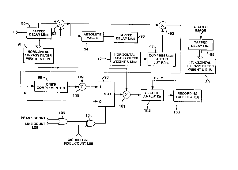
FIGURE 4 shows a multiply-tapped digital delay line 88
receiving the C, M & C IMAGE signal as its input signal. A weight-
and-sum circuit 89 weights signals from the taps of the delay line
88 so as to implement a horizontal low-pass filter with a cut-off
frequency of around 1.2 - 1.3 MHz providing a C&M signal response
substantially free of the 7.8 MH~ C IMAGE signal otherwise
accompanying the C signal as a result of the 4.2 MHz heterodyne in
the multiplier 82.
The L luminance signal, supplied during recording from the
cross-fader 69 i~n FIGURE 3, is applied in FIGURE 4 to a tapped
digital delay line 90. The delay line 90, a weight-and-sum circuit
91 and a digital subtractor 9~ arc connected to form a band splitter
filter that separates the L luminance signal into low-pass and high-
pass filter responses with a cross-over frequency of 2.52 Mhz or
one-quarter master clock sampling rate. The signals from the taps
of the delay line 90 are applied to the weight-and-sum circuit 91,
which generates the horizontal low-pass filter response. A digital
subtractor 92 subtracts the horizontal low-pass filter response
supplied by the weight-and-sum circuit 91 from suitably delayed L
signal taken from the tapped digital delay line 90, to generate the
horizontal high-pass filter response as the subtractor 92 difference
output signal.
As one skilled in the art of digital filtering appreciates,
digital band splitter filters are advantageous over analog band
splitter filters in that linear phase response through the region of
cross-over between the low-frequency and high-frequency bands is
readily obtained, which makes considerably simpler the rejoining of
the two bands later on. The phase linearity is achieved by making
the finite-impulse-response (FIR) low-pass filter comprising the
tapped delay line 90 and the weight-and-sum circuit 91 one with a
symmetrical weighting of the signals taken from the taps of the
delay line 90, in accordance with the customary horizontal low-pass
filter design procedure.
26 2~7~
A two-quadrant digital multiplier 93 multiplies the horizontal
high-pass filter response to L signal by factors less than one before
it is folded into baseband. This is done to compress the response
and attenuate it respective to the horizontal low-pass filter
response to L signal, which reduces the visibility of the reversed
frequency spectrum resulting from folding in television images
recovered from the video tape recording by VHS tape machines
already in the field. The multiplication factor used to compress the
horizontai high-pass filter response to L signal is determined as
follows. An absolute-value circuit 94 rectifies the horizontal high-
pass filter response to L signal. The rectified horizontal high-pass
filter response to L signal is supplied to a tapped digital delay line
95. The signals from the taps of the delay line 95 are applied to a
weight-and-sum circuit 96. The circuit 96 supplies a low-pass
filter response to the rectified horizontal high-pass filter response
to L signal, which response addresses a read-only memory 97 that
stores the multiplier signals supplied to digital multiplier 93 to
effect compression and attenuation of the horizontal high-pass
~ilter response to L signal.
Choosing the master clock sampling rate (which samples
luminance signals) to be twice the folding carrier frequency permits
the folding procedure to be irnplemented simply, without need for a
digital multiplier. The folded response to the band of compressed
and attenuated higher-frequency luminance components is generated
by a multiplexer 98, by alternately selecting at master clock
sampling rate either the current sample of the compressed and
attenuated horizontal high-pass filter response to L luminance
signal or its negative, as generated by applying each current sample
to a one's complementor 99 and augmenting the result by one in a
digital adder 100.
:' '~ "~ ' . " ; .
.
2~7~1~9~
-26a-
ln variants of the procedures described in the two paragraphs
immediately proceeding, the horizontal high-pass filter response to
L signal may be folded without its first being attenuated respective
to the horizontal low-pass filter response to L signal. This can be
done if there is no particular concern with providing backward
compatability of the video tape recording with folded-luminance
signal, in order to accomodate VHS tape machines already in the
field. Folding the horizontal high-pass filter response to L signal
without its first being attenuated can also be done without
sacrificing backward compatability, by subjecting the balanced
modulation signal from the multiplexer 98 to attenuation rather
than the horizontal high-pass filter response to L signal used as
modulating signal. This is done by supplying the balanc0d
modulation signal from the multiplexer 98 to elements
corresponding to elements 93-97 and connecting similarly with
~ach other and supplying the resulting attenuated balanced
,
:'~ ' ' ' ~ ' ' .
, ~ ,
20~ 1~9~
27
modulation signal to the adder 101 to be combined with the
horizontal low-pass filter response to L signal supplied from the
weight-and-sum circuit 91.
The band of higher-frequency luminance components folded
5 into baseband is supplied by the multiplexer 9~ as a summand input
signal to a digital adder 101, which receives from weight-and-sum
circuit 91 as its other summand input signal the band of lower-
frequency luminance components residual in the baseband. The adder
101 supplies its sum signal, the complete folded-luminance signal,
10 to a recording amplifier 102 in which that signal is subjected to
recording equalization, is converted to analog form, and then is used
to frequency-modulate (FM) a carrier occupying the 1.2 - 7.0 Mhz
band. The recording amplifier also receives the color-under carrier
that has been amplitude-modulated by C:&lll signal, which is
15 converted to analog form and combined with the frequency-
moduiated luminance carrier also in analog form to form a
composite signal applied to the helically scanning recording head(s)
103 of the video tape transport.
One skilled in the art of digital design will recognize that the
20 combination of elements 98-101 is what is commonly referred 7O
as a "controlled digital adder" or as a "digital adder/subtractor".
Without introducing much error, the output signal of the one's
complementor 99 may be applied directly to the mutiplexer 98
instead of through the adder 100 for augmenting by unity. In
25 another variation the adder 100 may augment the output signal of
the one's complernentor 99 by the control signal for the multiplexer
98 rather than unity.
The phase of the folding carrier used by the adder/subtractor
in generating folded-luminance signals reverses from one horizonta
30 scan line to the next within each field, and the pattern of phase
reversal is different in even frames than it is in odd frames. These
procedures reduce the visibility of the band of higher^frequency
luminance components folded into baseband in a teievision picture
recovered from the video tape recording. An exclusive-OR gate 104
35 receives the least-signi~icant bit of MODIJLO-320 PIXEL COUNT
as one of its two input signals, receives as its other input signal the
-
28 2~7~6
output signal of another exclusive-OR gate 105, and applies its
output signal as control signal to the multiplexer 98
The exclusive-OR gate 105 receives FRAME COUIJT as one of
its two input signals and the least-significant bit of LINE COUNT
5 as its other input signal. These signals do not change during the
duration of a horizontal scan line, so XOR gate 105 output signal to
the XOR gate 104 does not change during the duration of a horizontal
scan line. The least-significant bit of the MODULO-320 PIXEL
COUNT applied to the XOR gate 104 alternates between ZERO and
10 ONE at the 10.2 MHz master clock rate, however, thus conditioning
XOR gate 104 to supply to the multiplexer 98 a control signal that
also alternates between ZERO and ONE at the 10.2 MHz master clock
rate during each horizontal scan line, with a phasing dependent on
the XOR gate 105 output siynal maintained for the duration of that
15 scan line. The initial pixel of a scan line is associated with a ZERO
least-significant bit of the MODULO-320 PIXEL COUNT, as applied
as an input signal to the XOR gate 104.
In the following five paragraphs, the numbering of the
hcrizontal scan lines is described in terms of NTSC standard. During
20 an odd frame, when FRAME COUNT is ONE, the XOR gate 105 output
signal applied to the XOR gate 104 duplicates the least-significant
bit of LINE COUNT signal.
In the initial, odd field of an odd frame, the least-significant
bit of LINE COUNT is a ZERO during odd-numbered scan lines. This,
25 together with the ZERO least-significant bit of the MODlJLO-320
PIXEL COUNT for the initial pixel of a scan line, causes a ZERO XOR
gate 104 response that conditions the multiplexer 98 to select the
non-inverted folded high-frequency lurninance band for summation
with the low-frequency luminance band in the adder 101 during the
30 initial pixels of each of those odd-numbered scan lines.
In the initial, odd field of an odd frame, the least-significant
bit of LINE COUNT is a ONE during even-numbered scan ~ines. This,
together with the ZERO least-significant bit of the MODULO-320
PIXEL COUNT for the initial pixel of a scan line, causes a ONE XOR
35 gate 104 response that conditions the multiplexer 98 to select the
inverted folded high-frequency luminance band for summation with
" " , ,, ", " ,",",, ............ , ,~
.
29 2~7~1~9~
the low-frequency luminance band in the adder 101 during the
initiai pixels of each of those even-numbered scan lines.
In the final, even field of an odd frame, the least-significant
bit of LINE COUNT is a ONE during odd-numbered scan lines. This,
5 together with the ZERO least-significant bit of the MODULO-320
PIXEL COUNT for the initial pixel of a scan line, causes a ONE XOR
gate 104 response that conditions the multiplexer 98 to select the
inverted folded high-frequency luminance band for summation with
the low-frequency luminance band in the adder 101 during the
10 initial pixels of each of those odd-numbered scan lines.
In the final, even field of an odd frame, the least-significant
bit of LINE COUNT is a ZERO during even-numbered scan lines. This,
together with the ZERO least-significant bit of the R~ODULO-320
PIXEL COUNT for the initial pixel of a scan line, causes a ZERO XOR
15 gate 104 response that conditions the multiplexer 98 to select the
non-inverted folded high-frequency luminance band for summation
with the low-frequency luminance band in the adder 101 during the
initial pixels of each of those even-numbered scan lines.
During an even frame, when FRAME COUNT is ZERO, the XOR
20 gate 105 output signal applied to the XOR gate 1104 is the
complement of the least-significant bit of LINE COUNT signal,
reversing the initial pixel conditions for the horizontal scan lines in
an even frame from those specified above for an odd frame. Since
the pattern of phase reversal during folding of the luminance signal
~5 is different in even frames than it is in odd frames, it is necessary
to insert FRAME COUNT information into the recorded video signal
so that unfolding of the luminance signal during playback is done in
correct phasing, rather than the reverse phasing. This FFlAME
COUNT information can be inserted into the recorded video signai by
30 the sub-pixel phase reference generator 29 of FIGURE 1.
FIGURE 5 shows some of the playback electronics for the video
recorder in addition to the electronics shown in FIGURES 1 and 2,
which electronics are used both during recording and during
playback. Referring back to FIGURE 1, the DIGITAL VIDEO signal
3 5 supplied from the multiplexer 23 during playback is the di~itized
response of the analog-to-digital converter 7 to the ANALOG
2~7~a96
~IDEO signal that is luminance signal supplied from the playback
amplifier 4, owing to pole 2 of the record/playback switch being in
the playback position. The DIGITAL YIDEO signal supplied from the
multiplexer 23 is applied to a time-base corrector 106 during
5 playback. (By way of example, a time-base corrector can be a first-
in/first-out semiconductor memory, having a two sets of 640
storage locations alternately written and read each during the
course of a scan line. A line of 640 digital samples as timed by the
AFPC'd master clock oscillator 10 are written into the set of 640
1 û storage locations selected for writing during the current scan line.
Meanwhile the other set of 6~0 storage locations are sequentially
read from, as timed by a crystal-stabilized 10.2 MHz clook
oscillator. This crystal-stabilized 10.2 MHz clock oscillator is not
subject to the AFPC-loop errors and jitter introduced by tape
15 handling problems that can afflict the AFPC'd master clock
oscillator 10 during playback from a video tape recording.) The
resulting time-base-corrected DIGITAL VIDEO signal is supplied
from the time-base corrector 106 to a multiply-tapped digital delay
line 107. The signals from the taps of the delay line 107 are
2 0 applied to a weight-and-sum circuit 108, which innplements
horizontal low-pass filtering of the DIGITAL VIDEO signal that
supresses remnants of the frequency-modulation.
It is convenient to use digital filtering to perform the
playback equalization that compensates for the roll-off of Dl(iITAL
25 VIC)EO signal that would otherwise ocur because of bandwidth
limitations in the video tape recording procedure. FIGURE 5 shows,
in cascade connection after the horizontal low-pass filter
comprising elements ~07 and 108, a finite-impulse response
playback-equalization filter comprising a multiply-tapped digital
30 clelay line 152 and a weight-and-sum circuit ~53. The weights in
the weight-and-sum circuit 153 provide a peak around 3 MHz; and
the system charcteristic for the digital playback-equalization filter
may provide a raised-cosine response, by way of example. Rather
than using cascaded horizontal low-pass filter and playback-
35 equalization filters, cascaded as shown or in opposite order, a singledigital filter having a response similar to the product of the
:
31 ~7~
re~,~onses of the cascaded horizontal low-pass filter and playback-
equalization fi!ters can be used instead.
The time-base-corrected, horizontally iow-pass filtered
DIGITAL VIDEO signal with playback equalization is supplied to an
5 unfolding circuit comprising a muitiplexer 109 controlled by signal
generated by the XOR gateslO4 andlO5. The unfolded high-band
response to the time-base-corrected horizontally low-pass filtered
DIGITAL VIDEO signal is generated by the multiplexer 109, by
alternately selecting at master clock sampling rate either the
10 current sample of the time-base-corrected horizontally low-pass
filtered DIGITAL VIDEO signal signal or arithmetic zero.
The record/playback switch arranges (by connections of poles
thereof not explicitly shown in the drawing) that elements 54-69,
the same elements used for motion-adaptive spatio-temporal
15 filtering when recording, also provide a motion-adaptive spatio-
temporal filter 110 used during playback in a connection shown in
FIGURE 7. The motion-adaptive spatio-temporal filter 110
suppresses the folded-luminance components remnant in the
baseband after the unfolding procedure described above, as well as
2 0 "undoing" the motion-adaptive spatio-temporal filtering performed
during recording. The motion-adaptive spatio-temporal filter 110
requires for its operation that the MOTlt:)N signai used in the video
tape recording procedure be recovered and supplied thereto during
the video tape playback procedure. The recovery of MOTION signal
25 and the regeneration of color subcarrier modulation components
surrounding a suppressed 3.58 MHz color subcarrier, as done during
playback, are described immediately hereafter, with reference to
FIGURE 5.
An analog-to-digital converter 111 samples, at the 10.2 MHz
30 master clock rate, the color-under carrier as supplied from the
playback amplifier 4 shown in FIGURE 1. The converter 1 t 1 supplies
the digitized color-under carrier to a time-base corrector circuit
112. The resulting time-base-corrected, digitized color-under
carrier is supplied to a quadrant-selective filter 113. The
35 quadrant-selective filter 113 is a non-separable, two-dimensional
spatial filter that comprises tapped digital delay lines and a
2~7~9~
weight-and-sum circuit arranged for implementing a two-
dimensional kernel function for filtering three successive scan lines
of digitized coior-under carrier at the 10.2 MHz master clock
sampling rate.
FIGURE 6 diagrams this two-dimensional kernel function. The
filter l<ernel is of such breadth in ~he direction of horizontal scan
that only every fourlh column of coefficients is shown. The
intervening columns of coefficients are all columns of zero-valued
coefficients. The response of the quadrant-selective filter 113 is M
signal during odd fields and is C signal during even fields.
A subtractor 114 generates a complementary quadrant-
selective filter response by subtracting the response of the
quadrant-selective filter 113 from the time-base-corrected,
digitized color-under carrier supplied from the time-base corrector
112 and provided suitable compensating delay by digital delay line
115. This compensating delay equals the delay through the
quadrant-selective filter 113 and can be obtained using the tapped
digital delay lines in filter 113. The complementary quadrant-
selective filter response is C signal during odd fields and is M
signal during even fields.
A multiplexer 116 is conditioned by the least-significant bit
of the FIELD COUNT signal supplied thereto as its control signa! to
select from the quadrant-selective filter response and the
complementary quadrant-selective filter response, to generate a C
signal separated from M signal, and to generate an M signal
s~parated from C signal. An absolute-value circuit 117 rectifies
the M signal, and the rectified i\A signal is applied to the multiply-
tapped digitai delay line 118. The signals from the taps oF the delay
line 118 are applied to a weight-and-sum circuit 119, which
implements horizontal low-pass filtering of the rectified M signal
to regenerate the MOTION signal required by the motion-adaptive
spatio-temporal filter 110.
. , ,~ ' : ~ ', :
~7~96
-- 32~ -
The C signal separated from M signai is supplied from the
multiplexer 116 to a four-quadrant digital multiplier 120, there to
be multiplied for the duration of each scan line by the phase of the
four-phase 4.21 MHz carrier wave selected to it as multiplier signal
by the carrier-phase selection circuitry 83, thereby to regenerate a
digitized chroma signal comprising color subcarrier modulation
components surrounding a suppressed 3.58 MHz color subcarrier and
~7~
~3
their image components around 7.8 MHz. This digitized chrorna
signal is supplied as input signal to a multiply-tapped digital delay
line 121. A weight-and-sum circuit 122 weights signals from the
taps of the delay line 121 so as to implement a horizontal low-pass
5 filter providing color subcarrier modulation components surrounding
a suppressed 3.58 MHz color subcarrier, which filter response is
free from image components around 7.8 MHz. Alternatively, the
digital delay line 121 and weight-and-sum circuit 122 can be
replaced by a multiply-tapped digital delay line and a weight-and-
10 sum circuit that implement a digital band-pass filter with 3.58 MHz
center frequency. The delay line 121 and weight-and-sum circuit
122 may be arranged by suitable record/playback switching to be
the same as the delay line 88 and weight-and-sum circuit 89 used
during recording.
FIGURE 7 shows elements 54-64 and 67-69 which by suitable
record/playback switching (not explicitly shown) are arranged to
provide the motion-adaptive spatio-temporal filter 110 of FIGURE 5.
Usage of the elements 54-64 and 67-69 during both recording and
playback provides substantial savings in hardware costs by
20 eliminating one frame store and some line stores. Applying the
entirety of the frame-to-frame difference in luminance signal,
supplied from the weight-and-sum circuit 64, to the subtractor 67
as its subtrahend signal to be subtracted frorr luminance signal
supplied as its minuend signal from the delay line 60 removes
25 components all the way down in spatial frequency to zero Hz. This
is done reflective of the facts: (1) that the ~olded-luminance
components extend further down in frequency than chrominance
components; and (2~ that such frame combing, which is only possible
when NlOTiON signal is derived otherwise than as shown in FIGURE
30 3, provides a 3 dB reduction of low-spatial-frequency components.
During playback the cross-fader 69 is conlrolled by the regenerated
AIIOTION signal supplied from the weight-and-sum circuit 119 of
F3GURE 5. During lhe scanning of portions of the television image in
which there is considerable motion, the cross-fader 6g selects
3 5 spatially filtered luminance as its luminance output signal, as
supplied from the line-combing spatial filter comprising elements
,: -
'
,
~4 20 14~9~
-6 2 . This spatial filter provides vertical low-pass filtering that
suppresses the folded-luminance components remnant in the
baseband after unfolding, which remnant components change in
polarity from line to line. During the scanning of portions of the
television image in which there is little or no motion, the cross-
fader 69 selects temporally filtered luminance as its luminance
output signal, as supplied from the frame-combing temporal filter
comprising elements 54, 60, 66, 64, 67 and 68. The frame combing
suppresses the folded-luminance components remnant in the
baseband after unfolding, which remnant components change in
polarity from frame to frame.
If during recording the high-frequency band of the full-band
luminance signal supplied from the cross-fader 69 was de-
emphasized respective to its low-frequency band, the de-emphasis
is removed in circuitry comprising elements 1 23-1 31 . The removal
is done after separating this luminance signal into low-frequency
and high-frequency bands with filters having low-pass and high-
pass responses with a cross-over frequency of 2.52 Mhz or one-
quarter master clock sampling rate. The luminance signal supplied
during playback from the cross-fader 69 in FIGURE 5 is supplied to a
tapped digital delay line 123 in FIGURE 7. The signals from the taps
of the delay line 123 are applied to a weight-and-sum circuit 124,
which implements the horizontal low-pass filtering that separates
the low-frequency band component of luminance. A digital
subtractor 125 subtracts the hori~ontal low-pass filter response
supplied by the weight-and-sum circuit 124 from suitably delayed
full-band luminance signal taken from the tapped digital delay line
123, which implements the horizontal high-pass filtering that
separates the high-frequency band component of luminance.
A two-quadrant digital multiplier 126 multiplies the high-
frequency band component of luminance by factors greater than one
to de-compress that band and to restore it to its original amplitude
vis-a-vis the low-frequency band component of luminance. The
multiplication factor is determined as follows. An absolute-value
3 5 circuit 127 rectifies the high-frequency band component of
luminance supplied as difference signal from the subtractor 125.
, ., ... , ~ ~ ... ~.,.. ,.. , , -
~ ~ 7 ~
The rectified high-frequency band component of luminance is
supplied to a tapped digital delay line 128. The signals from the
taps oF the delay line 12~ are applied to a weight-and-sum circuit
129. Th0 circuit 129 supplies a low-pass filter response to the
rectified high-frequency band component of luminance, which
response addresses a read-only memory 130 that stores the
multiplier signals supplied to the multiplier 126 to de-compress
the high-frequency band component of luminance. The decompressed
high-frequency band component of luminance, supplied by the
10 multiplier 12~ as its product signal, is summed in a digital adder
~31 with the low-frequency band component of luminance, supplied
from the weight-and-sum circuit 124. The sum signal from the
adder 131 is a fully recovered luminance signal.
A digital adder 132 sums this signal with the chrominance
15 signal having a suppressed 3.58 MHz color carrier, as supplied from
the weight-and-sum circuit 122 of FIGURE 5. A digital adder 133
sums the sum signal ~rom the adder 132 with a sound subcarrier to
generate the modulating signal for a low-power television
modulator 134 used to generate television radio-frequency signals
2 0 for application to a color television receiver used for viewing
playback from a Yideo tape recording. The sound signal used to
frequency-modulate the sound subcarrier is either one that a
stationary audio playback head recovers from a lateral sound track
on the video tape recording or one that by helical scanning wide-gap
25 audio playback heads in the rotating headwheel assembly recover
from a deeply recorded diagonal sound track on the video tape
recording.
If during recording the high-frequency band of the full-band
lurninance signal supplied from the cross-fader 69 was not de-
3 0 emphasi~ed respective to its low-frequency band, the circuitry
comprising elements 1~3-131 can be replaced by a direct
connection ~rom the adder 73 to the adder 132.
The sub-pixel phase reference signal(s) may comprise selected
scan lines of repeated pseudo-random pulse sequences, which scan
3 5 lines occur during selected vertical trace intervals or within the
portions of the ima~e just thereafter which are masked so as not to
36 2~74~9~
be seen by a television viewer. Generally, the use of repeated
pseudo-random pulse sequences for time reference signals is well-
known. See, for example, pages 147-148 of W. Peterson's book
Error Correcting Codes, MIT Press, 1961; pages 655-657 of P.
Horowitz's and W. Hills's book The Art of Electronics, 2nd edition,
Cambridge University Press, 1989; pages 439-443 of F. G. Stremler's
book Introduction lo Communications Systems, 3rd edition,
Addison-Wesley Publishing Co., Reading MA, 1990; or the inventor's
and others' U. S. patent No. 4,912,549 issued 27 March 1990, entitled
1 0 "VIDEO SIGNAL SYNCHRONIZATION SYSTEM AS FOR AN EXTENDED
DEFINITION WIDESCREEN TELEVISION SIGNAL PROCESSING SYSTEM"
and assigned to RCA Licensing Corporation. The pseudo-random
pulse sequence is a string of -1 and +1 samples N in number which
exhibits a correlation of N with itself and correlations o~ unit value
15 with its phase-shifted self.
FIGURE 8 shows circuitry suitable for the sub-pixel phase
reference generator 24 in the FIGURE 1 video tape recorder
electronics. The FIGURE 8 circuitry includes a state-variable
generator 135 that generates fifteen consecutive pseudo-randorn
20 pulse sequences each seven samples long, the duration of each of
these samples being four times the interval between rnaster
oscillator 10 clock pulses, so as to keep the bandwidth of the
pseudo-random pulse pulses well within the bandwidth of the video
recording and playback procedures. The state-variable generator
25 135 includes three clocked bit latches 136,137, and 138 for
generating respective ones of three state variables. Each of the bit
latches 136, 137, and 138 is clocked with the carry signal from
the second stage o~ the FIGURE 1 nine-stage binary counter 11 as
generated every fourth master oscillator 10 clock pulse, so the
30 samples of the thre0 state variables each have durations which are
each four times the interval between master oscillator 10 clock
pulses. An exclusive-OR gate 139 receives state variables from the
latches 137 and 138 as its two input signals and supplies its
output signal as the input signal to the bit latch 136. The pseudo-
3 5 randorn pulse sequences supplied by the state-variable generator
135 issua from the bit latch 138 and are applied as input signal to
37 2~7~9~
_n exclusive-OR gate 140, which gate receives as the other of its
two input signals the rnodulo-two FRAME COUNT. During odd
frames XOR gate 140 response generates the negative of the pseudo-
random pulse sequences generated by the state-variable generator
135, and during even frames XOR gate 140 response simply repeats
the pseudo-random pulse sequences generated by the state-variable
generator 1 35.
The response of the XOR gate 140 is supplied as one of the two
input signals to an AND gate 141. The AND gate 141 selectively
10 repeats the response of the XOR gate 140 in its own response, which
is supplied as control signal to a multiplexer 142. Depending on
whether this control signal is ZERO or ONE, the multiplexer 142
chooses the digital value associated with û IRE level or with 80 IRE
level, thereby to generate the sub-pixel phase reference signal
15 supplied to the multiplexer 23 in FIGURE 1. The other input signal
to the AND gate 141 is a PULSE WINDOW signal that is ONE during
a period within a horizontal scan line when the pseudo-random pulse
sequences are supplied to the multiplexer 142. At the beginning and
at the finish of a scan line, when the PULSE WINDOW signal is a
20 ZERO, the response of the AND gate 141 is a ZERO, conditioning the
multiplexer 142 to choose the digital value associated with 0 IRE
level. The PULSE WINDOW signal corresponds to the set count (C;))
output of a set-reset flip-flop 143.
The setting and re-setting of flip-flop 143 proceeds as
25 follows. The SCAN-LINE PIXEL C:l:)UNT is augmented by two in a
digital adder 144 and the two least significant bits of the resulting
sum discarded to obtain a sparser count at one-fourth rnaster
oscillator 1~ clock pulse rate, which sparser count increments at
times between carry signals from the second stage of the counter
30 11. A decoder 145 decodes a beginning sparser count (e. ~., sixteen,
corresponding to a SC:AII-LINE PIXEL COUNT of sixty-two) to
generate a ONE supplied to OR gates 146-149. The ONE responses of
the OR gates 147,148 and 149 are supplied to the bit latches 136,
137 and 138, respectively, to be clocked thereinto so that the
35 initial pseudo-random pulse sequence always begins with ONEs in all
the bit latches 13B, 137 and 138. The ONE response of the OR gate
. .. . . , . . . ... ... ;.. .
,
:
2~7~9~
- 38
149 is supplied as a set pulse for the flip-flop 143, which fiip-flop
in its set state enables the AND gate 141 to supply pseudo-random
pulse sequences to the multiplexer 142. A decoder 150 decodes a
finishing sparser count (e. g., one hundred twenty, corresponding to a
5 SCAN-LINE PIXEL COUNT of four hundred seventy-eight) to
generate a reset pulse for the flip-flop 143. In its reset state, the
flip-flop 143 disables the AND gate 141, so it can no longer supply
pseudo-random pulse sequences to the multiplexer 142.
The connections described above lead to the following cycle of
10 operation, which repeats fifteen tinnes during the period that the
flip-flop 143 is set, generating a ONE as PULSE WINDOW signal.
39 2~7~96
LATCH LATCH LATCH - -
136 137 138
STATE STATE STATE
0
O 0
0 0
0 1 0
1 0
0
The 1110010 sequence supplied from the latch 138 may be
considered representative of the two's complement pseudo-random
15 pulse sequence 11,11,11,01,01,11,01 with the unchanging ONE
least-significant bit suppressed.
FIGURE 9 shows circuitry suitable for the sub-pixel phase
control circuitry 20 in the FIGURE 1 vi~eo tape recorder electronics.
A digital subtractor 154 receives, as its subtrahend input signal,
20 the digitized signal from the FIGURE 1 analog-to-digital converter 7.
A multiplexer 155 supplies the minuend signal for the subtractor
154 . An AND gate 156 responds with a ONi- to the P-B L-P-L KEY
signal generated by the FIGURE 2 AND gate 41 and the PULSE
WINDOW signal generated by the FIGURE 8 flip-flop 143
2 5 concurrently being ONEs, thereby to condition the multiplexer 155
to select the digital value associated with a 40 iRE level as minuend
signal for the subtractor 154, which biases the pseudo-random -
pulse sequences so as to have a zero-valued direct component.
During most scan lines, when the P-B L-P-L KEY signal is
30 ZERO, and during th~ beginning and finish of those once-in-a-frame
scan lines, when the P-B L~P-L KEY signal is ONE but the PULSE
WINIDC)W signal is ZERO, the AND gate 156 responds with a ~ERO,
conditioning the multiplexer ~ 55 to seleet the digitized signal from
the FIGURE 1 analog-to-digital converter 7 as minuend signal for the
35 subtractor 154. The subtractor 154 generates a zere-valued digital
difference signal responsive to its subtrahend and minuend signais
being the same.
~' ' . ,
:': . . .: ,: .
~ ' ' ' ' ' ,
. , :
~7~9~
A 28-sample correlation filter 1~7 receives from the
subtractor 154 the pseudo-random pulse sequences biased so as to
have a zero-valued direct component. When the correlation is best
between the input signal and the filter kernel, or when anti-
correlation is best between the input signal and the filter kernel,
the filter 157 correlation response will be twenty-eight times as
large as the signal supplied thereto from the subtractor 154 and
thus will have five rnore bits than the digitized signal from the
analog-to-digital converter 7. The filter 157 response will be
thirteen bits wide, assuming the ADC 7 digitizes with eight bits
resolution. To conserve hardware, the four least-significant of
these bits are not used in the subsequent circuitry. The filter 157
response is supplied to an absolute-value circuit 158, to generate a
one-bit-narrower absolute-value correlation response that is
supplied to a cascade connection of parallel-bit registers 1 59 and
160. The cascade connection of parallel-bit registers 159 and 160
provides a three-tap delay that permits three consecutive
correlation responses to be considered at ~ time. When circular
correlation of the correlation filter 157 kernel and the pseudo-
random pulse se~uence from the subtractor 154 is reached, the
response of the filter 157 exhibits a positive peak that extends over
more than one sample at master oscillator clocking rate, owing to
the fact that the pseudo-random pulse rate is one-quarter the
master oscillator clocking rate. When circular anti-correlation of
2 5 the correlation filter 157 kernel and the pseudo-random pulse
sequence from the subtractor 1~4 is reached, the response of the
filter 157 exhibits a negative peak that extends over a similar
small number of samples. The peak can be considered to extend over
seven samples, or over just ~ive samples.
In any case, three consecutive ones o~ these samples will be
considered to constitute the tip of the peak, and analysis of the
three samples at each tip of a correlation peak (or anti-correlation
peak) is used to determine how closely the timing of the digitization
process by the analog-to-digital converter 7 during playback
corresponds to the timing of the dlgitization process by the analog-
to-digital converter 7 during recording. If the correspondence is
41 20~ 9 ~
perfect, the two samples preceding and succeeeding the maximum-
amplitude very-tip sample will be of equal amplitudes somewhat
smaller than the maximum-amplitude sample that they flank. If the
timing of the digitization process by the analog-to-digital converter
S 7 during playback leads the timing of the digitization process by theanalog-to-digital converter 7 during recording, the sample preceding
the maximum-amplitude very-tip sample is smaller in amplitude
than the sample succeeeding the maximum-amplitude sample. If the
timing of the digitization process by the analog-to-digital converter
7 during playback lags the timing of the digitization process by the
analog-to-digital converter 7 during recording, the sample preceding
the maximum-amplitude very-tip sample is larger in amplitude than
the sample succeeeding the maximum-amplitude sample.
The current sample D Srom the register 160, the current
sample E from the register 159 and the current sample F from the
absolute-value circuit 158 are the three consecutive correlation
responses that are considered at any one time. A digital comparator
161 generates a ONE when and only when E~D; a digital comparator
162 generates a ONE when and only when E~F; and a digital
comparator 163 generates a ONE when and only when E~ET, where ET
is a prescribed positive threshold value. An AND gate 164 responds
to the three comparators 161-163 all generating ONEs at the same
time with a ONE indicative that the current sample E is a maximum-
amplitude, very-tip sample~
A digital comparator 165 g0nerates a ONE when and only
when D~F, indicating that the timing of the digitization process by
the analog-to-digital converter 7 during playback leads the timing
of the digitization process by the analog-to-digital converter 7
during recording. A digital comparator 166 generates a ONE whPn
and only when F~D, indicating that the timing of the digitization
process by the analog-to-digital converter 7 during playback lags
the timing of the digitization process by the analog-to-digitai
converter 7 during recording. An OR gate 1~7 receives the output
signals from the comparators 165 and 166 as its input signals and
generates a ZERO when and only when D-F, indicating that the timing
of the digitization process by the analog-to-di~ital converter 7
.. . ...
;. . ' , ' .. `.`.'.,`.'.. " ~,`.. `'
a,2 ~7~96
during playback properly corresponds to the timing of the
digitization process by the analog-to-digital converter 7 during
recording. (Each of the digital comparators 161~163, 165 and 166
is of a general type generating a ONE when and only when an A input
5 signal thereto exceeds a B input signal thereto. Such a comparato
is provided by a digital subtractor receiving its A and B input
signals as two's complement subtrahend and minuend signals,
respectively, with the sign of the difference providing the
comparison result.)
An AND gate 168 responds to AND gate 164 generating a ONE
indicative that the current sample E is a maximum-amplitude
sample and to OR gate 167 generating a ONE indicative that the
current D and F samples differ in amplitude to generate a ONE that
is an indication of a need to correct the phasing of luminance pixels
during playback. A five-stage up/down binary counter 169 counts
the number of these indications. The counter 169 is reset to an
initial value of sixteen by the decoder 145 or the decoder 146
output signal pulsing to ONE. The output signal from the comparator
165 controls the direction of counting by the counter 169.
2 0 When the timing of the digitization process by the analog-to-
digital converter 7 during playback leads the timing of the
digitization process by the analog-to-digital converter 7 during
recording, the counter 169 counts down, responsive to the
comparator 165 output signal be!ng a ONE. When the timing of the
2 5 digitization process by the analog-to-digital converter 7 during
playback lags the timing of the digitization process by the analog-
to-digital converter 7 during recording, the counter 169 counts up,
responsive to the comparator 165 output signal being a ZERO.
An OR gate 172 responds, either to a one count from the
counter 169 being detected by a decoder 170 or to a thirty-one
count from the counter 169 being detected by a decoder 1Y1, to
generate a ONE. During playback this ONE alters by one the count in
an up/down binary counter ~73, used ta control the multiplexer 21
shown in FIGURE 1 as selecting the tap of the tapped digital delay
line 19 from which the master oscillator clocking pulse is taken for
application to the analog-to-digital converter 7. The counter 169
2~7~3~6
~3
receives the most-significant or ~sign" bit from the counter 16 9
count as its up/down control signal. Accordingly, the thirty-one
count from the counter 169, indicative of fifteen consecutive
indications of leading luminance-pixel phase during playback, causes
5 the count from the counter 173 to increment by one, in turn causing
the multiplexer 21 to select the master oscillator clocking pulses
applied to the analog-to-digital converter 7 from a next-later tap on
the multiply-tapped digital delay line 19. And the one count from
the counter 169, indicative of fifteen consecutive indications of
10 lagging luminance-pixel phase during playback, causes the count
from the counter 173 to decrement by one, in turn causing the
multiplexer 21 to select the master oscillator clocking pulses
applied to the analog-to-digital converter 7 from a next-earlier tap
on the multiply-tapped digital delay line 19.
During recording, the counter 173 is continuously reset to
arithmetic zero, to force the multiplexer 21 to select a middle tap
of the multiply-tapped digital delay line 19.
FIGURE 9 also shows how the modulo-two frame counter 37
(also shown in FIGURE 2) is arranged to be correctly phased during
20 playback, so the pattern of luminance pixel sampling corresponds to
that used during recording. An up/down binary counter 174 counts
the number of positive or negative peaks in t'ne correlation f~nction
during a scan line when P-B L-P-L KEY signal is ONE. Like the
counter 169, the counter 174 is reset to an initial value of sixteen
25 by the decoder 145 or the decoder 146 output signal pulsing to ONE.
The pulsing of the AND gate 164 response to ONE, signalling sample
E being a very-tip sample in the correlation response, is counted by
counter 174. The sign bit of the response from the correlation
filter 157 is extracted and is delayed one pixel duration in a bit
30 latch 175 clocked at the 10.2 MHz master clock oscillator pulse
rate. The bit temporarily stored in the bit latch 175 corresponds to
the sign of the sample having sample E as its absolute value, is
temporally aligned with sample E, and controls the direction of
counting by the counter 174.
During a scan line in an odd frame which scan line spans a
period when P-B L-P-L KEY signal is ONE, the response from ths
.
~ ' ~
4 4 ~ 2 ~
correlation filter 157 should have fifteen negative-going peaks
Accordingly, the bit temporarily stored in the bit latch 175 should
be a ONE when the counter 174 counts each very-tip sample, which
up/down signal from the bit latch 17~ conditions the counter 174
for counting downward. Supposing the counter 174 counts
downward by fifteen from its initial value of sixteen, a decoder 176
detects the resulting one count to generate an indication that
FRAME COUNT should be odd, or ONE. An AND gate 177 ANDs the
decoder 176 output signal with the complement of FRAME COUNT
to generate a ONE indicating when FRAME COUNT is even when it
should be odd. An OR gate 178 responds to any ONE generated by the
AND gate 177 to generate a ONE as CORRECT FRAME signal for
application via the OR gate 179 as a count input signal to the
counter 174 to exchange the logic states of its its modulo-two
count output signal FRAME C:OUNT and its other modulo-two count
output signal that is the complement of FRAME COUNT.
During a scan line in an even frame which scan line spans a
period when P-B L-P-L KEY signal is ONE, the response from the
correlation filter 157 should have fifteen positive-going peaks.
Accordingly, the bit temporarily stored in the bit latch 175 should
be a 7ERO when the counter 174 counts each very tip sample, which
up/down signal from the bit latch 175 conditions the counter 174
for counting upward. Supposing the counter 174 counts upward by
fifteen from its initial value of sixteen, a decoder 189 detects the
resulting thirty-one count to generate an indication that FRAME
CC)UNT should be even, or ZERO. An AND gate 181 ANDs the decoder
180 output signal with FRAIAE COUNT to generate a ONE indicating
when FRAM COUNT is odd when it should be even. The OR gate 178
responds to any ONE generated by the AND gate 181 to generate a
ONE as CORRFCT FRAME signal for application via the OR gate 17g
as a count input signal to the oounter 174 to exchange the logic
states of its its modulo-two count output signal FRAME CC)UNT and
its other modulo-two count output signal that is the complement of
FRAME COIJNT.
FIGURE 10 shows a representative structure for the FIGURE 9
correlation filter 157, which digital filter structure i5 of the
2~74'~
,..,~)ut-waighted type, with +1 anà -1 filt0r coefficients. The two's
complement input signal to the correlation filter from the
subtractor 154 is input-weighted by the filter coefficient -1 by
complementing each of its bits in a one's complementor circuit 182
and using a digital adder 183 for adding arithmetic one to the output
signal from the one's complementor circuit 182. A 28-tap digital
delay line is formed from elements 184-237, the even-numbered
ones of these elements being word latches clocked by the 10.2 MHz
master clock oscillator pulses and the odd-numbered ones of these
elements being digital adders each receiving its addend from the
word latch with next lower numbering than its own. Each of the
adders in this 28-tap digital delay line except adder 237 supplies
its sum signal to the word latch with next lower numbering than its
own. The two's complement input signal to the correlation filter
1 5 from the subtractor 154 is inherently input~weighted by the filter
coefficient +1, is supplied to the word latch 184 at the beginning of
the 28-tap digital delay line, and is applied as augend input signal to
each of the digital adders 191, 187,189, 215, 217, 219, 221,
223, 225, ~27 and 229. The two's complement input signal to the
correlation filter from the subtractor 1 S4, as input-weighted by the
filter coefficient -1, is supplied as sum signal from the adder 183
and is applied as augend input signal to each of the digital adders
191, 193, 195, 197, 199, 201, 203, 205, 207, 209. 211, 213,
231, 233, 235 and 237. The adder 237 supplies its sum signal, as
2 5 the response of the correlation filter 157 to the absolute-value
circuit 1 58.
Referring back to FIGURE 4, there are numerous alternative
circuits that may replace th~ balanced modulator circuit comprising
elements 98-101,104 and 10~. Elements 98 and 9g are the
equivalont of a digital subtractor with a wired two as subtrahend.
Elements 98~101 are often considered tog~ther as a group, forming
a digital adder/subtractor that adds its data input signals
responsive to a ZERO control signal and that subtracts one of its
data input signals ~rom the other responsive to a ONE control si~nal.
FIGURES 11-14 each show a balanced modulator alternative to
that shown in FIGURE 4, in which elements 98 and 99 are replaced
2~7~
46
by the equivalent digital subtractor 23B with a wired two as
subtrahend, in which the XOR gates 104 and 105 are not used, and in
which the mutiplexer 100 is replaced by a cascade of three
multiplexers, the first two of which 239 and 240 are of "double-
pole-double-throw switch" type and the last of which 240 is of
"single-pole-double-throw switch" type. In FIGURES 11 and 12 the
first multiplexer 239 reverses the polarities of its output signals
responsive to the least-significant bit of the MODULO-~20 PIXEL
COUNT. In FIGURE 11 the second multiplexer 240 reverses the
polarities of its output signals responsive to LINE COUNT, and the
third multiplexer 241 reverses the polarities of its output signals
responsive to FRAME CC)UNT; in FIGURE 12 the second multiplexer
240 reverses the polarities of its output siynals responsive to
FRAME COUNT, and the third multiplexer 241 reverses the
polarities of its output signals responsive to LINE COUNT. It is
advantageous from the standpoint of the power consumption
attendant with the switching of the multiplexers 239, 240 and 241
that multiplexer 241 which is of "single-pole-double-throw switch"
type be the fastest switched.
FIGURES 13 and 14 show the MODULO-320 PIXEL COUNT
controlling the switching of the third multiplexer 241. In FIGURE
13 the first multiplexer 239 reverses the polarities of its output
signals responsive to LINE COUNT, and the second multiplexer 240
reverses the polarities of its output signals responsive to FRAME
CQUNT; in FIGURE 14 the first multiplexer 239 reverses the
polarities of its output signals responsive to FRANIE COUNT, and
the second multiplexer 240 reverses the polarities of its output
signals responsive to LINE COUNT. Two additional permutations of
the control signal connections of the multiplexers 239, 240 and
241 are possible, in each of which permutations the second
muliplexer 240 is controlled by the MODULO-320 PIXEL COUNT.
Any cascade of just two of the multiplexers 239, 240 and 241 can
be replaced by a single muliplexer controlled by exclusively ORing
the two of the FRAME COIINT, LINE COUNT, and MODULO-320
PIXEL COUNT signals other than the one controlling the other
multiplexer.
47 2~7~9~
In FIGURES 15-18 the baianced modulator is subsumed into the
circuitry for combining the low-pass-filtered component and the de-
emphasized high-pass-filtered component of the luminance signai
during the folding procedure In each of the FIGURES 15-18 a digital
5 adder 243 additively combines the low-pass-filtered component of
the luminance signal, supplied from the weight-and-sum cirGuit 91,
with the de-emphasized high-pass-filtered component of the
luminance signal supplied as product output signal from the digital
multiplier 93. The digital adder 243 generates a weighted sum of
10 the low-pass-filtered and high-pass-filtered components of the
luminance signal, with the low-pass-filtered component accorded a
positive weight of one, and with the digital multiplier 9 3
determining the positive weight accorded to the high-pass-filtered
component. In each of the FIGURES 15-18 a digital subtractor 244
15 receives as its subtrahend input signal the iow-pass-filtered
component of the luminance signal from the weight-and-sum circuit
91, and receives as its minuend signal the de-emphasized high-
pass-filtered component of the luminance signal from the digital
multiplier 93 The digital subtractor 244 generates a weighted sum
20 of the low-pass-filtered and high-pass-filtered components of the
luminance signal, with the low-pass-filtered component accorded a
positive weight of one, and with the digital multiplier 9 3
determining the negative weight accorded to the high-pass-filtered
component. Selection at pixel rate between the adder 243 sum
25 signal and the subtractor 244 difference signal generates folded-
luminance signal for application to the record amplifier 102. With
regard to the low-pass-filtered component of the luminance signal
supplied from the weight-and-sum circuit 9t, which is a single-
ended component of the modulating signal, the modulation procedure
30 carried out by the modulation circuitry of any of the FIGURES 15-18
is balanced only inasfar as the folding carrier frequency is
concerned.
In FIGURES 15 and 16 the selection at pixel rate between the
adder 243 sum signal and the subtractor 244 difference signai is
35 done by the cascaded rnultiplexers 239-241. There are four other
permutations of applying the three control signals FRAME CC)UNT,
. .. , .. ,.. : . . , .... _,.,~
. . . .. . ...... .....
48 2~7~
Ll~ COUNT LSB, and MODULO-320 PIXEI COUNT LS~ to the
multiplexers 239-241 in stiil other embodiments of the invention.
FIGURE 17 shows a variant of FIGURE 15 (or 16) in which the
cascaded multiplexers 239 and 240 are replaced by a single
5 multiplexer 245 controlled by the XOR gate 105 response to control
signals FRAME COUNT and LINE COUNT LSB. The cascaded
multiplexers 240 and 241 in the FIGURE 15 modulator circuitry are
replaced by a single multiplexer controlled by the response of an
exclusive-OR gate receiving FRAME COUNT and MODULO-320
10 PIXEL COUNT LSB input signals in another embodiment of the
invention not shown in the drawing. In yet another embodiment of
the invention not shown in the drawing, the cascaded multiplexers
240 and 241 in the FIGURE 16 modulator circuitry are replaced by a
single multiplexer controlled by the response of an exclusive-OR
15 gate receiving LINE COIJNT LSB and MODULO-320 PIXEL CC)UNT
LSB input signals.
FIGURE 18 shows the selection at pixel rate between the adder
243 sum signal and the subtractor 244 difference signal being done
by a single multiplexer 246, with selection being controlled by the
20 XOR gates 104 and 105 responsive to the three control signals
FRAME COUNT, LINE COUNT LSB, and MODULO-320 PIXEL COUNT
LSB.
The operation of the balanced modulator in the video recording
system described in U. S. patent application serial No. 787,690 for
2 5 various relationships between the folding frequency and the
sampling rate of the luminance signal is illustrated by the frequency
spectra of FiGURES 19-24 sharing the same axis of abscissas in
frequency, the frequency spectra of FIGURES 25-30 sharing the same
axis of abscissas in frequency, and the frequency spectra of FIGURES
30 31-36 sharing the same axis of abscissas in frequency.
FIGURE 19 depicts the frequency spectrum of a fuil-band
luminance signal in which digitization is ~arried out at a rate three
times a 5.1 MHz folding carrier frequency. In addition to the
baseband subspectrum extending from zero to 5MHz, there are
35 subspectra that are first-harmonic sidebands of the 15.3 MHz
luminance sampling carrier, the lower sideband extending down from
4~ 2~7~96
,.3 MHz to 10.3 MHz and the upper sideband extending up from 15.3
MHz to 20.3 MHz. There will also be sidebands flanking the higher
harmonics of the sampling carrier, which additional subspectra are
not of consequence here and are ignored.
FIGURE 20 depicts the frequency spectrum of the response, of a
digital low-pass filter with 2.55 MHz cut-off, to the FIGURE 19 full-
band luminance signal spectrum in which digitization is carried out
at a rate three times the 5.1 MHz folding carrier frequency. In
addition to the baseband subspectrum extending from zero to 2.55
A~Hz, there are subspectra that are first-harmonic sidebands of the
15.3 MHz luminance sampling carrier, the lower sideband extending
- down from 15.3 MHz to 12.75 MHz and the upper sideband extending up from 15.3 MHz to 17.85 MHz.
FIGURE 21 depicts the frequency spectrum of the response, of a
digital high-pass filter with 2.55 MHz cut-off, to the FIGURE 19
full-band luminance signal spectrum in which digitization is carried
out at a rate three times the 5.1 MHz folding carrier frequency. In
addition to the baseband subspectrum extending from 2.55 to 5 MHz,
there subspectra that are are first-harmonic sidebands of the 15.3
MHz luminance sampling carrier, the lower sideband extending down
from12.75 to 10.3 MHz and the upper sideband extending up from
17.85 to 20.2 MHz.
FIGURE 22 depicts the frequency spectrum resulting from
balanced modulation of a 5.1 MHz folding frequency carrier by the
FIGURE 21 digital high-pass filter response. The baseband
subspectrum extending from 2.55 to 5 MHz is heterodyned by the 5.1
MHz folding frequency carrier to generate a reversed-spectrum
lower sideband extending down from 2.55 to 0.1 MHz and to generate
an upper sideband extending up from 7.65 to 1û.1 MHz. The lower
3 0 first-harmonic sideband in the 10.3-12.7~ MHz band is translated to
a 5.2-7.65 Hz band and a 15.4-17.85 MHz band. The upper first-
harmonic sideband in the 17.35-20.3 MHz is translated to a 12.25-
10.2 Hz band and a 22.45-25.4 MHz band (off the drawing to the
right) .
FIGURE 23 depicts the frequency spectrum resulting from
adding the spectra of FIGURES 20 and 22. There are gaps in the
... .. ..
.: . . ~,
. ~ ... . -- -
,
- . - :' :
:
. .
,,
~7~
FIGURE 23 spectrum in the bands where the FIGURE 19 high-pass
filter responses reposed. These gaps are 2.5 MHz wide so that a
low-pass filter with a cut-off frequency in the 2.55-5.1 MHz range
is easily designed to suppress the subspectra in the 5.2-10.1 MHz
5 band and their harmonics.
FIGURE 24 depicts the frequency spectrum resulting from low-
pass filtering the FIGURE 23 spectrum, the subspectra of which are
converted to analog low-pass filter response by a digital-to-analog
co nverter.
FtGURE 25 depicts the frequency spectrum of a full-band
luminance signal in which digitization is carried out at a rate 2.5
times a 5.1 MHz folding carrier frequency. In addition to the
baseband subspectrum extending from zero to 5MHz, there are
subspectra that are first-harmonic sidebands of the 12.75 MHz
luminance sampling carrier, the lower sideband extending down from
12.75 MHz to 7.75 MHz and the upper sideband extending up from
12.75 MHz to 17.75 MHz. There will also be sidebands flanking the
higher harmonics of the sampling carrier, which additional
subspectra are not of consequence here and are ignored.
FIGURE 26 depicts the frequency spectrum of the response, of a
digital low-pass filter with 2.55 MHz cut-off, to the FIGURE 25 full-
band luminance signal spectrum in which digitization is carried out
at a rate 2.5 times the 5.1 MHz folding carrier frequency. In addition
to the baseband subspectrum extending from zero to 2.55 MHz, there
are subspectra that ar~ first-harmonic sidebands of the 12.75 MHz
luminance sampling carrier, the lower sideband extending down from
12.75 MHz to 10.2 MHz and the upper sideband extending up from
12.75 MHz to 15.3 MHz.
FIGURE 27 depicts the frequency spectrum of the response, of a
digital high-pass filter with 2.55 MHz cut-off, to the FIGURE 25
full-band luminance signal spectrum in which digitization is oarried
out at a rate 2.5 times the 5.1 MHz folding carrier frequency. In
addition to the baseband subspectrum extending from 2.55 to 5 MHz,
there subspectra that are are first-harnnonic sidebands of the 12.75
MHz luminance sampling carrier, the lower sideband extending down
: .
51 2~7~96
tromlO.2 to 7.65 MHz and the upper sideband extending up from 15.3
to 17.85 MHz.
FIGURE 28 depicts the frequency spectrum resulting from
balanced modulation of the 5.1 MHz folding frequency carrier by the
5 FIGURE 27 digital high-pass filter response. The baseband
subspectrum extending from 2.~5 to 5 MHz is heterodyned by the 5.1
MHz folding frequency carrier to generate a reversed-spectrum
lower sideband extending down from 2.55 to 0.1 MHz and to generate
an upper sideband extending up from 7 65 to 10.1 MHz. The lower
10 first-harmonic sideband in the 7.65-10.2 MHz band is translated to a
2.55-5.1 MHz band and a 12.75-15.3 MHz band. The upper first-
harmonic sideband in the 15.3-17.85 MHz is translated to a 10.2-
12.75 Hz band and a 20.4-22.95 MHz band (off the drawin~ to the
rig ht) .
1 5 FIGURE 29 depicts the frequency spectrum resulting from
adding the spectra of FIGURES 26 and 28. There are no gaps in the
FIGURE 29 spectrum in the bands where the FliURE 27 high-pass
filter responses reposed, so that a low-pass filter with a very sharp
cut-off frequency of 2.55 MHz is required to suppress the subspectra
20 in the 2.55-5.1 MHz band and their harmonics.
FIGURE 30 depicts the frequency spectrum resulting from low-
pass filtering the FIGURE 29 spectrum, the subspectra of which are
converted to analog low-pass filter response by a digital-to-analog
converter. The low-pass filtering with a very sharp cut-off
25 frequency of 2.55 MHz tends to make the cross-over from the 0-2.55
MHz portion of the unfolded luminance signal to its 2.55-5.1 MHz
portion other than smooth because of the usual loss of some of the
energy around the 2.55 lAHz cross-over frequency.
As the sampling rate of the luminance signal becomes less
30 than 2.5 times tha ~olding frequency, the subspectra of the high-
pass filter response in the baseband and in the lower first-harmonic
side~and of the sampling frequency when heterodyned with 5.1 MHz
foldin~ carrier generate, by their respective down-conversions in
frequency, overlapping subspectra in the bas~band. This is an
35 aliasing that cannot be undone. Surprisingly, however, when the
sampling rate of the luminance signal is exactly twice ghe folding
:. , ,.. , . . ... ~. ~
52 2~7~
carrier frequency -- i. e., exaclly the Nyquist limit iowest sampling
rate -- the aliasing of the lo~er first-harmonic sideband of the
sampling frequency into the baseband is no longer a problem, since
this alias exactly repeats and reinforces the folded high-pass filter
response in the baseband.
FIGURE 31 depicts the frequency spectrum of a full-band
luminance signal in which digitization is carried out at a rate twice
a 51 MHz folding carrier frequency In addition to the baseband
subspectrum extending from zero to 5MHz, there are subspectra that
are first-harmonic sidebands of the 10.2 MHz luminance sampling
carrier, the lower sideband extending down from 10.2 MHz to 5.2 MHz
and the upper sideband extending up from 10.2 MHz to 15.2 MHz.
There will also be sidebands flanking the higher harmonics of the
sampling carrier, which additional subspectra are not of
consequence here and are ignorecl.
FIGURE 32 depicts the frequency spectrum of the response, of a
digital low-pass filter with 2.55 MHz cut-off, to the FIGURE 31 full-
band luminance signal spectrum in which digitization is carried out
at a rate twice the 5.1 MHz folding carrier frequency. In addition to
the baseband subspectrum extending from zero to 2.55 MHz, ther~
are subspectra that are first-harmonic sidebands of the 10.2 MHz
luminance sampling carrier, the lower sideband extending down from
10.2 MHz to 7.65 MHz and the upper sideband extending up from 10.2
MHz to 12.75 MHz.
FIGURE 33 depicts the frequency spectrum of the response, of a
digital high-pass filter with 2.55 MHz cut-off, to the FIGURE 31
full-band luminance signal spectrum in which digitization is carried
out at a rate twice the 5.1 MHz folding carrier frequency. In addition
to the baseband subspectrum extending from 2.55 to 5 MHz, there
subspectra that are are first-harmonic sidebands of the 10.2 MHz
luminance sampling carrier, the lower sideband extending down from
7.65 to 5.2 MHz and the upper sideband extending up from 12.75 to
15.2 MHz.
FIGURE 34 depicts the frequency spectrum resulting from
balanced modulation of a 5.1 MHz folding frequency carrier by the
FIGURE 33 digital high-pass filter response. The baseband
2~7~6
aspectrum extending from 2.55 to 5 MHz is heterodyned by the 51
MHz folding frequency carrier to generate a reversed-spectrum
lower sideband extending down from 2.55 to 0.1 MHz and to generate
an upper sideband extending up from 7.65 to 10.1 MHz. The iower
5 first-harmonic sideband extending down from 7.65 to 5.2 MHz is
translate~ to generate a reversed-spectrum lower sideband
extending down from 2.55 to 0.1 MHz; and the upper first-harmonic
sideband extending up from 12.75 to 15.2 MHz is translated to
generate a subspectrum extending up from 7.65 to 10.1 MH~. These
10 aliases of the first-harmonic sidebands are identical to the result
of folding the high-pass filter response baseband component. During
playback, then, there is no need to separate these aliases from the
result of folding the high-pass filter response baseband component
and discard them.
FIGURE 35 depicts the frequency spectrum resulting from
adding the spectra of FIGURES 32 and 34. There are gaps in the
FIGURE 34 spectrum in the bands where the FIGURE 33 high~pass
filter responses reposed. These gaps are 2.5 MHz wide so that a
low pass filter with a cut-off frequency in the 2.55-5.1 MHz range
20 is easily design to suppress the subspectra in the 5.2-10.1 MHz band
and their harmonics.
FIGURE 36 depicts the frequency spectrum resulting from low-
pass filtering the FIGURE 35 spectrum, the subspectra of which are
converted to analog low-pass filter response by a digital-to-analog
2 5 converter.
While the invention has been described with particular
reference to the context of providing improved VHS recording, the
invention provides solution to other problems concerning restricted-
bandwidth media for the transmission of video information. For
30 example, the invention can be useful in the tape recording of high-
definition or extended-definition television signals, whether such
recording is done on an analog basis or on a digital basis. In such
embodiments of the invention, appropriate modifications are made
to accomodate the use of progressive frame scanning rather than the
35 scanning of interleaved scan fields in each frame.