Note : Les descriptions sont présentées dans la langue officielle dans laquelle elles ont été soumises.
~ 207469 1
The present invention relates to an information reproducing circuit for use in
information recording-reproduction apparatuses such as magneto-optical recording-
reproduction apparatuses.
One prior art magnetic head dnving circuit using a magnetic field modulation
system is described in Japanese Laid-Open Patent Application No. 63-94406. The
following description will discuss this prior art system in detail.
When a 2-7 RLL code, shown in Figure 10(3) of the accompanying drawings,
is recorded using the NRZI recording system, a bit "1" reverses the direction of the
recording current of a magnetic head. In a magnetic head driving circuit as shown in
Figure 9, the reversing of the recording cunrent is conducted by switches 6 and 7.
More specifically, when the switch 6 is tumed on (see Figure 10(b)) with the
switch 7 off (see Figure 1 0(c)), a current l1 fiows from a dc power source 3 to ground by
way of an auxiliary coil 2 and the switch 6. Also a cunrent 12 fiows from a dc power source
5 to ground by way of an auxiliary coil 4, a magnetic head coil 1 and the switch 6. Each
time the switches 6 and 7 are reversed, an induced high voltage appears at a connecting
point Q between the auxiliary coil 4 and the switch 7. As a result, a driving current lx,
different from the cun-ent 12, flows through the magnetic head coil 1 in a direction from Q
to P.
On the other hand, when the switch 7 is turned on with the switch 6 tumed off
(see Figure 10(b) and (c)), the current 12 of the auxiliary coil 4 flows to ground from the dc
power source 5 by way of the auxiliary coil 4 and the switch 7. The current 11 of the
auxiliary coil 2 flows to ground from the dc power source 3 by way of the auxiliary coil 2,
the magnetic head coil 1 and the switch 7. Each time the switches 6 and 7 are reversed,
a high induced voltage appears at the connecting point P between the auxiliary coil 2 and
the switch 6. As a result, a driving current lx, diflerent from the current 11, flows through
the magnetic head coil 1 in a diredion from P to Q.
Fi~;ure 10(h) and (g) ~ ,e~,~i.r~ly indicate loads in response to "on" and "off'positions of the switches 6 and 7 when the coil 1 is seen from the side of the auxiliary coils
2 and 4. As illustrated in these drawings, the load varies between the value of the
impedance (Zx) of the coil 1 and zero. However, the inductance (Lx) of the coil 1 is set
to be substantially smaller than the inductance (Ld) of the auxiliary coils 2 and 4. That is,
the setting is made to satisfy: Lx Ld. Therefore, if Lx = o, then Zx = 0. That is, the
C,`
~, 20 7469 ~
load when seen from the side of the auxiliary coils 2 and 4 becomes virtually zero; thus,
the variation of the load can be virtually ignored.
By the use of the above-mentioned magnetic head driving circuit, i"ru"" "- l
is recorded, for example, by forming recording marks on a magneto-optical disk. The
5 recorded information is then reproduced by an information reproducing circuit in response
to a readout signal derived from these recording marks. An example of such an
i, ~fJI " IdLiul) reproducing circuit is described in Japanese Laid-Open Patent Application No.
1-1 3658.
This infommation reproducing circuit is provided with a positive peak-hold circuit
10 and a negative peak-hold circuit. A slice signal is formed by the addition of outputs from
both peak-hold circuits in an à,Upl u,ul idte ratio (for example, 1:1). The level of the readout
signal is compared with that of the slice signal; thus, a binary signal is extracted from the
readout signal.
However, in the above-mentioned conventional magnetic head driving circuit,
15 when there is a difference in ske between the level of the positive "o",,uollel,~ and that of
the negative uOIIl,uol~elll of the driving cunrent lx through the coil 1 (that is, a lack of
balance), the distance between zero-crossing points in the driving current l~ deviates and
the magnitude of generated magnetic felds in the positive direction and the negative
direction become different from each other. As a result, jitter of the recording marks
20 increases.
This problem becomes more obvious in the case where the NRZI recording
system for 2-7 RLL code is adopted as a modulation system of the magneto-opticalrecording-reproduction apparatus. This system, although having an advantage that the
recording density can be increased, suffers from the disadvantage that a large dc
25 uulll,uOI~ell~ is present in the recording current. Therefore, if a recording signal obtained
by this system is applied to the co,~ .,' ,al magnetic head driving circuit, the above
problem is inevitably present.
Moreover, when it is desired to increase the frequency of the recording signal
in order to enhance the data transfer rate, Ld should be minimi~ed. As Ld is reduced, it
30 du,uluaulles the level of Lx. This results in variation of the loads.
Consequently, as illustrated in Figures 10(d) and 10(e), the balance of the
currents 1, and 12 is upset, thereby resulting in a difference ~llel~ . Since the
distance between zero-crossing points in the driving current l~ deviates and the " ,a~ des
- 2 -
.,
(~ 7
207469 1
of the driving cun-ent IK in the positive direction and the negative direction become different
from each other, jitter of the recording marks increases, thereby reducing the reliability of
reproduced data.
More specifically, in the case where the positive col",uol~"~ and the negative
5 uu"",ulle"l of the driving current l~ of the coil 1 are different from each other in size, if
recording marks (indicated by a solid line in Figure 11(c)), which have been recorded
according to 2-7 RLL code (see Figure 11 (a)), are read out by an optical head (not shown),
a readout signal, indicated by a solid line in Figure 11 (d), will be obtained.
On the other hand, in the case where the positive ..u,, ,,uu, ,e"~ and the negative
10 ,u" l~,oll~. ,l of the driving current lx of the coil 1 are of the same size (that is, they balance
each other), if recording marks (indicated by a dashed line in Figure 11(c)) are read out
by the optical head (not shown), a readout signal, indicated by a dashed line in Figure
11(d), will be obtained.
In a Cull~ dl information reproducing circuit, a slice signal is obtained by
15 the use of peaks in the positive direction and in the negative direction of an input signal.
For example, when the slice signal is formed by using an il lL~ idlc: level between the
peak in the positive direction and the peak in the negative direction (see Figure 11 (d)), an
output signal (see Figure 11 (e)) of a bUlll,Udld~UI (not shown) contains jitter to an extreme
extent. In cu",,ua,i:,ol- with the case where the positive cu"",ùlle"l and the negative
20 uui~,uollelll ofthe driving cunrent l~ balance each other, a penod of "1" ofthe output signal
ofthecu,,,,ud,dLu, isshortenedwhileaperiodof"0"thereofisle"uLl,el1ed. Thisconstitutes
one of the reasons that reproduced data is distorted.
Additionally, the above example describes the case where recording marks are
shorter than non-recording marks; however, in contrast thereto, another case may be
2~ considered, wherein recording marks are longer than non-recording marks. Here, in
bOlll~dli~UI~ with the case where the positive ,ulll~,oll~lll and the negative co",,uul,~"l of
the driving cun-ent l~ balance each other, the period of "1" of the output signal of the
,~llI,UdldLUr is lel~uLl,~,,ed while the period of "0" thereof is shortened.
Furthenmore, the above example describes the case where the slice signal is
3û obtained from the illL~ idL~ level between the peak in the positive direction and the
peak in the negative direction. However, in another case, if a slice signal obtained by
addition of the peaks in the positive direction and in the negative direction in an
.Itplupidl. -tio,isused,ino~he~wods i~a~liw~ign-lh~ving.l evelth~tdevi~tesr~m
2074691
the ill~ ldid~t~ level is used, jitter will be reduced in either "0" or "1"; however, jitter will
be increased in the other of "1" or "0".
It is an object of the present invention to provide an il~rulllld~iun reproducing
circuit for accurately converting a signal, read out from a recording medium, into a binary
signal.
Accordingly, the invention provides an information reproducing circuit for
converting into binary digits a reproduced signal read out from a recording medium
whereon illfUlllld~iul~ has been recorded as a recording signal by a recording means, and
said reproducing circuit having an amplitude jitter eliminating means for receiving said
reproduced signal and fûr eliminating jitter therefrom which is related to amplitude
variations in said reproduced signal as compared to said recording signal and for removing
low frequency co",,uo"e"~:, sup~,i",uosed upon the readout signal, and phase jitter
eliminating means for receiving said reproduced signal and eliminating jitter therefrom, said
jitter is related to phase variations in said reproduced signal as compared to said recording
signal, said reproducing circuit including a subtracting circuit receiving as inputs an output
of said amplitude jitter eliminating means and an output of said phase jitter eliminating
means; and a CUlll~dldlUI receiving as inputs said reproduced signal and an output of said
subtracting circuit.
In auuulddl~c~ with the above dlldllg~lllelll, a signal read out from the
recording medium, even if jitter is contained therein, can be accurately converted into
binary digits. Therefore, reliability of the reproduced data can be enhanced.
For a fuller ul1d~l ,ldl~i"g of the nature and ad~/dllld~ps of the invention,
reference will be made to the ensuing detailed description taken in conjunction with the
acu~",ud"Ji.,g drawings, in which:
Figures 1 through 7 illustrate a first e",l,o.li",~l,l of the present invention;Figure 1 is a circuit diagram illustrating a main part of an illrUlllldli
reproducing circuit of a magneto-optical recording-reproduction apparatus;
Figure 2 is a diagram illustrating an equivalent circuit of a magnetic head
driving circuit and a magnetic head coil of Figure 1;
Figure 3 is a circuit diagram illustrating a filter circuit of Figure 1;
Figure 4 is a diagram illustrating waveforms of respective parts of Figure 1;
Figure 5 is an explanatory diagram illustrating the, ~Id~iUI Isl ,i~ between ~lx and
QT in Figure 4;
-4 -
C,
207469 1
Figure 6 is a diagram illustrating waveforms of the signals obtained when
reproduction is conducted by the infonmation reproducing circuit of Figure 1 distorted by
frequency transfer functions of the magnetic head driving circuit and the magnetic head
coil;
Figure 7 is a diagram illustrating wavefomms of the signals of Figure 6 in detail;
Figure 8, which shows a second e",~odi",e"l of the present invention, is a
circuit diagram illustrating a main part of an information reproducing circuit of a magneto-
optical recording-reproduction apparatus;
Figures 9 through 11 show an apparatus of the prior art;
Figure 9 is a circuit diaqram illustrating a conventional magnetic head driving
circuit and a conventional magnetic head coil;
Figure 10 is a time diagram illustrating wavefomms of the signals of Figure 9;
and
Figure 11 is a time diagram illustrating waveforms of signals of a conventional
illfUlllldliull recording-reproduction circuit
Referring to Figures 1 through 7, the following description will discuss the first
el"bo~i",~"l of the present invention.
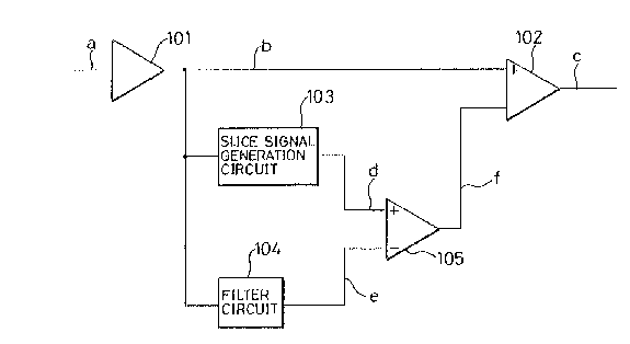
Figure 1 illustrates an information reproducing circuit of a magneto-optical
recording-reproduction apparatus of the present invention.
A readout signal a from a magneto-optical recording medium is amplified by
an amplifier 1û1. An output signal b from the amplifier 1û1 is sent to the positive input
temminal of a C,Ulll,Udld~UI 102, a slice signal generation circuit 103 and a filter circuit 104.
In the slice signal generation circuit 103, a slice signal d is generated in a.,-,u,ddl-c~ with
the output signal b. The output signal b is subject to distortion by the fluctuation of mark
lengths caused by the frequency response ,l Idldulel i~liG of a magnetic head driving circuit
including a coil 1 of a magnetic head.
As illustrated in Figure 6(a), a driving current l~, which flows through the coil
1 of the ma~netic head, varies dependent on the various positioning of the recorded data.
This is because the frequency response el ,a, dulel i:,~i.. of the magnetic head driving circuit
3û including the coil 1 of the magnetic head are expressed by a frequency transfer function
of an equation (3), which will be described later. v'vhen the waveform of Figure 6(a) is
reformed so as to make the level of its envelope constant, a waveform having a variation
in its zero level is obtained, as shown in Figure 6(o). Here, an optimal zero level is located
-- 5 --
~ I
~i
207469 1
in the center between the positive and negative envelopes, as is given by a dashed line
in Figure 6(b).
The variation of the zero level causes the length of recording marks fonmed
on the magneto-optical disk to vary. That is, when the zaro level is lowered (see a portion
5 indicated by Y in Figure 6(b)), the recording marks become longer than a p,~dc L,~ ed
length. vAvhen the zero level is raised (see a portion indicated by X in Figure 6(b)), the
recording marks become shorter than the p,~del~""il1ad length.
Figure 2 is a diagram of an equivalent circuit of a conventional magnetic head
driving circuit (see Figure 9). Resistors R in Figure 2 indicate the total equivalent
10 resistance of the switch 6 and the dc power source 3 and the total equivalent rasistance
of the switch 7 and the dc power source 5. Voltage V (volt) is the output voltage of the dc
power sources 3 and 5.
First, Z, and Z2 are deflned as follows:
Z1 = R + i ~
Z2 = R + i'~ L2 + j",-Ll ~ (2)
where L, is the inductance of the coil 1; L2 iS the inductance of the auxiliary
coil 2 as well as the auxiliary coil 4; ca is the angular frequency; and j = (-1)%.
In Figure 2 and Figure 4(b), currents having positive and negative directions
applied to the coil 1 of the magnetic head are respectively designated as 1, and 12. These
20 cun-ants are equivalent to respective average currents in the auxiliary coil Z and the
auxiliary coil 4. The time ratio dunng which the cunrent flows from the auxiliary coil 2 to
the ground terminal is designated as ~ and the time ratio during which the current flows
from the auxiliary coil 2 to the coil 1 of the magnetic head is l~,ult:Se~ d by (1 - O The
average current 1, in the auxiliary coil 2 is I~ tnl~ by:
/1 = 1~ x ( V) + (1-1~) x (z~)
Also, the average cunrent 12 in the auxiliary coil 4 is l~,,t,s~"t- d by:
-- 6 -
~;
2o746g 1
/2 = (1 -1~) X (Z ) (Z )
Since the deviation ~lX of the driving current lx is l~p,~se"Lt:d by the difference between
these values, the following equation holds:
l2)
= V X (~_1 ) X ( 1 _ 1 )
v'vhen the dc component of the driving current lx is zero, a = (1 - a) that is, a
= 1/2. Therefore, I~lx = 0 holds. Here, for convenience of explal~d~iul~, a is given as the
time ratio with respect to the dc cu",~,ol~e"l of the driving current lx; yet, in fact, it is given
as the time ratio with respect to the low frequency .,~",~-ol~e"L of the driving current lx.
Equation (3) is a frequency transfer function of the magnetic head driving
circuit and the magnetic head coil.
Figure 3 shows one example of a circuit configuration of the filter circuit 104
which is anranged to have the same frequency transfer fundion as that of the circuit of
Figure 2. More specifcally, the filter circuit 104 comprises a coil 403 having the
inductance L" coils 404 and 405, both having an inductance L2, resistors 406 and 407
having a resistance R, a subtracting amplifier 401 and a variable resistor 4û2. The coil
4û3 is connected in series with the coil 404. One end of these coils 403 and 404 is
connected to a negative input terminal of the subtracting amplif er 401 while the other end
thereof is connected to the output of the amplifier 101. One end of the coil 405 is
conneded to a positive input terrninal of the subtracting amplifier 4û1 while the other end
2û thereof is connected to an output of the amplifier 1û1.
The negative input terminal of the subtracting amplifier 401 is connected to
ground through the resistor 406. The positive input terminal of the subtracting amplifier
4û1 is connected to ground through the resistor 407. On the other hand, the output of the
subtracting amplifier 401 is connected to ground through the variable resistor 402, so that
- 7 -
207469 1
an output signal e (that is, an output of the hlter circuit 104) is obtained on the variable
resistor 402.
By ~ " ' ,g the voltage of the output signal b from the amplifier 101 as Vjn
and the voltage of the output signal e of the filter circuit 104 as VO~ and the total
cl,,, '- ' 1 of the subtracting ampliher 401 with the variable resistor 402 as o, the
following equation (4) holds:
Vin (Z1 Z )
where Z, and Zz ,t,s,ue.,.;,~cly satisfy the foregoing equations (1) and (2).
The equation (4) is a frequency transfer function of the filter circuit 104; thus,
by adjusting o a~l,,up,i~ ,ly, the equation (4) becomes virtually equal to the frequency
transfer function of the magnetic head dnving circuit including the coil of the magnetic head
shown in Figure 9. Therefore, an output that is formed in accu,dd,~, with the frequency
transfer function of the magnetic head driving circuit including the coil of the magnetic head
is obtained from the hlter circuit 104.
The slice signal d released from the slice signal generating circuit 103 is sentto the positive input terminal of a subtracter 105, while the output signal e of the filter
circuit 104 is sent to the negative input terminal of the subtracter 105. The output of the
subtracter 1û~-f, i.e. a slice signal f, obtained by subtracting the output signal e from the
slice signal d, is sent to the negative input terminal of the uulll~Jaldtul 102. The
I,UIllUdl~VI 102 compares the levels of the slice signal f and the output signal b and
produces a digital signal c.
Refening to Figures 6 and 7, the following description will discuss the
operation of the information reproducing circuit of the magneto-optical recording-
reproduction apparatus of the present invention.
The slice signal d is generated in the slice signal generating circuit 1û3 in
accu,ddllu~, with the output signal b of the amplifier 101 (see Figure 6(c)). On the other
hand, the output siSfnal b is applied to the filter circuit 104, and processed into the signal
e having a waveform as shown in Figure 6(d) because the filter circuit 104 has
substantially the same frequency transfer function as the magnetic head driving circuit
including the coil of the magnetic head.
8 -
_~,
207469 1
The output signal e of the filkr circuit 104, after having undergone subtractionfrom the slice signal d in the subtracter 105, forms the slice signal f (see Figure 6(e))
whichisappliedtothenegativeinputterminaloftheuu",~,d,dIu, 102. TheGolll~Jdld~ol 102
compares the levels of the slice signal f and the output signal b and produces a digital
5 signal c.
For example, when a recording mark (see Figure 7(a)), which has been
recorded with a longer time than a pl~dc~I~,,,,i,,ed value, due to variation of the driving
current l~ caused by the frequency transfer function of the magnetic head driving circuit
including the coil 1 of the magnetic head, is reproduced, the reproduced signal (the output
10 signal b of the amplifier 101) has a peak whose duration is generally longer than a
~ ,~dc~ ""i"ed value. However, in acuu,ddn,,e: with the present invention, the slice signal
f derived from this recording mark with a longer duration becomes larger (see Figure 7(b)
and the portion indicated by Y' in Figure 6(e)), and thus the recording mark is reproduced
as a peak with a shorter width. Therefore, as a result, a mark signal (digital signal c)
15 similar to that obtained when the recording mark with the pl~deLt~ lilled length is
reproduced can be obtained (see Figure 7(c)).
On the other hand, when a recording mark (see Figure 7(a)), which has been
recorded with a shorter duration than a p, e.lt,Ic~ ed value is reproduced, the reproduced
signal (the output signal b of the amplifier 101) has a peak whose duration is generally
20 shorter than a p,~ ""i"ed value. However, in auuo,~d"ce with the present invention,
the slice signal f obtained from this recording mark having the shorter duration becomes
smaller (see Figure 7(b)). Thus, the portions indicated by X' in Figure 6(e), and thus the
recording mark are reproduced as a peak with a longer width. As a result, a mark signal
(digital signal c) similar to that obtained when the recording mark with a ,ulede~ illed
25 length is reproduced can be obtained (see Figure 7(c)).
In Figure 7(a) dashed lines indicate recording marks, having a ,ult:deLt:lllli"ed
length, which will be fonmed where there is no fluctuation in the driving cun~ent l~. Dashed
lines in Figures 7(b) indicate a slice signal d.
As described above, since the frequency tra nsfer ul Idl dU~ liu of the magnetic30 head driving circuit including the coil 1 of the magnetic head is COI I l,U~l~Sd~d, it is ensured
that jitter in the digital signal c, that is, in an output signal of the CUlll,.)dldLUr 102, can be
reduced even if jitter occurs in the recordi ~a ~arks.
. ~
2 0 7469 1
Refen-ing to Figure 4, the following description will discuss a circuit operation
of Figure 1.
When the 2-7 RLL code of Figure 4(a) is recorded on a magneto-optical
recording medium by the use of the NRZI recording system, the driving current lx (indicated
5 by a solid line in Figure 4(b)) is displaced along the y-axis by ~ , due to the influence of
the frequency transfer ~;I,a,aulc"i~l;u of the magnetic head dnving circuit including the coil
1 of the magnetic head in colll,udliaoll with a normal level (indicated by a dashed line in
Figure 4(b)). This ~ia,ula~ ll causesthe recording marks to be lellu~ll,t:"~d (indicated
by solid lines in Figure 4(c)) and the wavefomm of the readout signal is thus vaned
10 (indicated by solid lines in Figure 4(d)).
In order to (iulll,u~llS..~k for this di~,ulac~,,,~,.,l, the slice signal f (indicated by
a solid line in Figure 4(d)) is displaced accordingly with respect to the slice signal d
(indicated by a dashed lined in Figure 4(d)). Therefore, a jitter ~T (indicated by a dashed
line in Figure 4(e)), appears in the output signal c when the ~iul, lUdl ~ Ul 102 compares the
output signal b and the slice signal d. However, the jitter (indicated in Figure 4(e)), which
appears in the output signal c when the uu,, I,Udl d~Ol 102 compares the output signal b and
the slice signal f, is positively reduced.
Figure 5 shows the results of measurements with respect to the ~ sl ,i,u
between the deviation l~IK of the driving current l~ and the jitter QT of the output signal c.
I~T, is a jitter uulll,uol~lll in I~T that occurs due to deviations of the spacebetween zero-crossing points of the dnving cunrent l~. On the other hand, I~Th is a jitkr
cOIll,uol~elll in ~T that occurs due to differences in the magnitudes of magnetic helds
generated in the positive direction and the negative direction. The following equation (5)
shows the l~ldliUll~l~iU between ~T, I~T, and l~Th:
~ T = ~ T~ Th -- (5)
As shown in Figure 5, ~T is directly l ,v,uu,liu"al to al~. In other words, ~
occurs due to the frequency transfer ulldlduL~lialiu of the magnetic head driving circuit
including the coil 1 of the magnetic head; and ~T is thus produced in proportion to 1~
Theuu,,,,u~, " nisprovidedfortheslicesignaldbytheuseofthehltercircuit104and
the subtracter 105 and the UUIllUdld~Ul 102 compares the output signal b and the slice
signal f in their levels; this plupolliu,,~ reduces ~T.
- 10-
C
207469 1
More specihcally, the frequency transfer function of the magnetic head driving
circuit including the coil 1 of the magnetic head, shown in Figure 2, is arranged to be
substantially identical to the Frequency transfer function of the filter circuit 104, shown in
Figure 3; and bullluel~sdliull is provided for the sum of u,upo,liol~al .u~rri.i~"L~ of the
above functions by the use of the variable resistor 4û2. Thus, these operations make it
possible to Culll,u~ for l~T which has the same phase as the driving current 1~1~ and
is u,upu~liunal thereto~
For convenience of I~AUIdl I " 1, Figure 4 uJ~el 1 l, ''~ '~ only the case where the
recording marks are set to be shorter than the non-recording marks. However, the present
invention is not l1eu~aadl;~y limited to this dlldll9Ulllellll, and depending on data, is
adaptable for another dlldil~Ullltllll where the recording marks are longer than the non-
recording marks. In this case, the same effect as in the present e",bodi",~"l can be
obtained although the readout signal a and the output signal G are inverted.
Figure 8 illustrates the second e",bo.li,l,al,l of an infonmation reproducing
circuit of a magneto-optical recording-reproduction apparatus of the present invention.
Here, those membens that have the same functions and that are described in the hrst
~",L,o.li",e"l are indicated by the same reference numerals and the description thereof is
omitted .
The present er"L,r,di",~"l is different from the first ~",L,o.li",~"l in that the
2û output signal c from the UlllUdldlUI 102 is applied to the hlter circuit 104 rather than the
output signal b from the amplifier 101.
By applying the output signal c of the COlll,UdldlUI 102 to the hlter circuit 104,
it is ensured that the influence of the frequency tnansfer characteristic of the magnetic head
driving circuit including the coil 1 of the magnetic head, which is contained in the output
signaI c, can be c~",u~,~ ad L~d. Therefore, as with the hrst e" ,L,o~i" ,e"I, this dl I dl l~U,~11 ,al,L
makes it possible to remarkably reduce jitter in the output signal c of the ,UllI,UdldLUr 102,
even if jitter occurs in the recording marks.
- 11 -
~,~