Note : Les descriptions sont présentées dans la langue officielle dans laquelle elles ont été soumises.
7-5027
A CONCENTRATOR-BASED GROWABLE PACKET SWITCH
Technical Field
This invention relates to packet switching and, more particularly, to a
growable packet switch architecture.
Background of the Invention
Growable packet switch architectures are known in the art. These prior
known architectures, however, were implemented by employing a plurality of mxn
(m > n) Packet Switch Units. Although the use of mxn Packet Switch Units has
heretofore made sense for growth to a larger packet switch, the individual Packet
Switch Units still have to meet the requirement of being stand-alone Packet Switch
Modules upon initial deployment. A prior growable packet switch architecture is
disclosed in United States Patent 4,955,017 issued to K.Y. Eng, M.J. Karol and Y.S.
Yeh on September 4, 1990. As such, the Packet Switch Unit would only have to have
an equal number of inputs and outputs. In other words, an mxn Packet Switch Unit can
only be used as an nxn Packet Switch Module upon initial installation. Deploying a full
mxn Packet Switch Unit to be used as an nxn Packet Switch Module is wasteful andexpensive. Indeed, such a development would incur unnecessary technical and financial
risk. Thus, although the prior known mxn Packet Switch Units are satisfactory for
certain applications, they are not satisfactory for use as stand-alone nxn Packet Switch
Modules.
Summary of the Invention
The problems and limitations with prior mxn Packet Switch Units are
overcome, in accordance with the principles of the invention, by employing a unique
Concentrator-Based Packet Switch Unit. To this end, an m:n Concentrator arrangement
followed by an nxn Packet Switch Module is advantageously employed, in accordance
with the invention, to realize the desired mxn Packet Switch Unit architecture.
In accordance with one aspect of the invention there is provided an mxn
(m > n) packet switch unit, where m is an integer of at least two (2) and n is an integer
of at least one (1), comprising: a packet cell concentrator having m inputs and n outputs
including means for temporarily storing arriving packet cells on the m concentrator
inputs and means for supplying all of said arriving packet cells in a prescribed repetitive
sequence to the n conce~ Alor outputs, said means for temporarily storing arriving
~ 2075027
- la-
packet cells including means for temporarily storing arriving packet cells on the m
concentrator inputs in arriving packet cell time slots in excess of available packet cell
positions in the n concentrator outputs in output packet cell output time slots so that
packet cells of any such excess of said arriving packet cells are not lost or discarded;
5 and a packet switch module having n inputs and n outputs for supplying the packet cells
being supplied from the n outputs of the concentrator to the n inputs of the packet
switch module to appropriate ones of the n outputs of the packet switch module in
accordance with an assigned destin~tion address carried by the individual packet cells.
In accordance with another aspect of the invention there is provided in
10 an mxn (m > n) packet switch unit, where m is an integer of at least two (2) and n is
an integer of at least one (1), a method colllplisillg the steps of: concentrating packet
cells arriving on m inputs to n outputs of an m:n (m > n) concentrator includingtemporarily storing arriving packet cells on the m concellLIdlor inputs and supplying all
of said arriving packet cells in a prescribed repetitive sequence to the n concentrator
15 outputs, said step of temporarily storing arriving packet cells including temporarily
storing arriving packet cells on the m concentrator inputs in arriving packet cell time
slots in excess of available packet cell positions in the n concentrator outputs in output
packet cell output time slots so that packet cells of any such excess of arriving packet
cells are not lost or discarded; and switching the packet cells being supplied from the n
20 outputs of the concentrator to n inputs of an nxn packet switch module to applopl;-dte
ones of n outputs of the packet switch module in accordance with an assigned
destination address carried by the individual packet cells.
~ - .
j~r
C _
2075027
- 2 -
A plurality of the resulfing Concentr~tor-Based mxn Packet Switch
Units can readily be employed to realize a larger packet switch, as desired.
A technical advantage of this invention is that a stand-alone nxn Packet
Switch Module can be initially deployed and, then, the m:n Concçntrator can be later
5 deployed to grow into a packet switch having a larger number of m inputs.
Brief Description of the D~ ~wil.~,
In the drawing:
FIG. 1 shows, in simplified block ~ ~m form, an embo 1iment of the
invention incl~1fling an m:n Concentrator in combhlation with an nxn Packet Switch
10 Module;
FIG. 2 depicts, in simplified block diagram form, details of the m:n
ConcentratorofFM. l;
FIG. 3 graphically illustrates in a simplified llal~r the operation of the
concentrator of FIG. 2;
FIG. 4 depicts, in simplified block diagram form, a mxm packet switch
(m=32 as an example) formed by employing the invention of FIG. l;
FIG. 5 shows, in simplified block diagram form, a larger packet switch
(64 x 64 as an example) using a variation of the invention shown in FM. l;
FIG. 6 depicts, in simplied block diagram form, a generalized version of
20 an NxN packet switch matrix using the principles of the invention; and
FIG. 7 shows, in simplified block diagram form, an embo lim~nt of a
"large" concenl. ~tOl based on "smaller" con~e ~ tor m xl~ s
Detailed Description
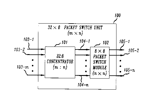
FIG. 1 shows, in simrlified block ~ ~m form, an embo~liment of the
25 invention employing m:n ConcenL.~lor 101 in colllbinalion with nxn Packet Switch
Module 102 to form mxn Packet Switch Unit 100. As in(lic~tç~ above it, is
advantageous to be able to deploy nxn Packet Switch Module 102 as a stand-alone
module and later grow, it in accordance with the inventionj to mxn Packet SwitchUnit 100. Again, this is realized, in accordance with the invention, by the unique
30 ufili7~tion of a prior known nxn Packet Switch Module 102 and, then, employing
m:n Concen~.ator 101 with it at a later date. The nxn Packet Switch Module 102
interrogates each a~iving packet cell for its (3estin~tion address and then routes it to
the appl~liate one of outputs 105-1 through 105-n. Multiple arriving packet cells
destined for the same one of outputs lQ5 are allowed, and queuing is provided in35 Packet Switch Module 102 to buffer the multiple arriving packet cells properly so
2075027
~_ - 3 -
that they can be applu~liately read ûut at the destin~tion output one (1) packet cell at
a time. Many techniques are known for implem~nting Packet Switch Module 102.
However, employing a shared lllelllUl,~ technique is plefe~ d. As in-lir~te~, Packet
Switch Module 102 may be one of known such mod~lles (see for example, United
5 States Patent 4,603,416). As shown, Concentrator 101 has inputs 103-1 through
103-m and outputs 104-1 through 104-n which are supplied as inputs to Packet
Switch Module 102. In turn, Packet Switch Module 102 has outputs 105-1 through
105-n. In the specific example shown in FM. 1, m=32 and n=8, so that Concentrator
101 is a 32:8 (m:n) concentrator and Packet Switch Module 102 is an 8x8 (nxn)
10 switch forming 32x8 (mxn) Packet Switch Unit 100.
FIG. 2 shows, in simplified form, details of one implel..enlalion of
Conce~ or 101 of FM. 1. Specific~lly, shown is random access lll~llUl~ (RAM)
201 and control unit 202. RAM 201 is employed as a shared Ille~llUl,~ having m
inputs 103-1 through 103-m (m=32 in this e~mple) and n outputs 104-1 through
15 104-n (n=8 in this ex~mple) to form under control of control unit 202 the desired
m:n Concel-tlatol 101. It is noted that a multiplexer (not shown) is typically used to
supply packet cells from inputs 103 to RAM 201 and that a ~emllltiplexer (not
shown) is typically used to supply packet cells from RAM 201 to outputs 104.
Control unit 202 effects the writing of arriving packet cells from inputs 103 into
20 RAM 201 and the reading of packet cells from RAM 201 to outputs 104 in the ~l~O
sequence. It should be noted that Concen~tor 101 operates in a simpler manner
than a packet switch. Unlike a packet switch, Concelll.ator 101 does not e~minç
the address of each arriving packet cell. Its function is merely to concenl ate all
incoming packet cells to be supplied to outputs 104 on a first-in first-out (FIFO)
25 basis. In this eY~mple up to m (m=32) packet cells may arrive in one packet cell
interval, i.e., time slot, but only n (n=8) packet cells can be supplied as outputs
during a packet cell interval, i.e., time slot. The excessive packet cells are buffered
tel~.alily in RAM 201 for FIFO operations. The long term average loading on
Concenllator 101 cannot exceed the output capacity of its n outputs, but
30 inst~n~neous fluctuations, of course, render the burre.i-lg of packet cells in RAM
201 necessary.
FIG. 3 graphically illustrates the first-in first-out (FIFO) operation of
RAM 201 under control of control unit 202 in re~li7ing Concen~tor 101 of FIG. 1.For clarity and brevity of description a 4:2 "first-in first-out" (FIFO) concentrator
35 arrangement is described. It will be al~pdl~llt to those skilled in the art how to
expand the described concentrator operation to a 32:8 concelltl~lol or any size
2075027
-
- 4 -
concentrator, as desired. It is also noted that arriving packet cells in excess of the
number of output lines to the concent,~tor are temporarily buffered. In this example,
the arriving packet cells on inputs 301-1 through 301-4 are supplied to outputs 302-1
and 302-2 in a predeterminP(l repetitive sequence. Specifir~lly, the predeterminçd
5 sequence in a particular time slot starts with any packet cell arriving on input 301-1
through any packet cell arriving on 302-4 and is repeated for each successive time
slot. Thus, as shown in FIG. 3, packets are shown as arriving on inputs 301-1
through 301-4 in time slots 0 through 3 and are labeled accordingly. As shown,
packet cells 0 arrive on inputs 301-1, 301-2 and 301-4 in input time slot 0. The10 arriving packet cell 0 on input 301-1 is immetli~tely supplied to output 302-1 in
output time slot 0 and the arriving packet cell 0 on input 301-2 is imm~li~tçly
supplied to output 302-2 in output time slot 0. The arriving packet cell 0 on input
301-4 must be te.l~ol~;ly stored in RAM 201 (I;IG. 2) and, then, supplied to output
302-1 in the next output time slot, namely, output time slot 1. The packet cells15 arriving in input time slot 1 on inputs 301-2 through 301-4 are accordingly labeled 1.
The packet cell 1 arriving on input 301-2 is immP~ tely supplied to output 302-2 to
be output in time slot 1. The packet cells 1 a~iving on inputs 301-3 and 301-4 are
temporarily stored in RAM 201 to be supplied to outputs 302- 1 and 302-2,
respectively, in output time slot 2. The arriving packet cells on inputs 301-1 through
20 301-3 in input time slot 2 are tel~ol~ily stored in RAM 201 to be supplied tooutputs 302-1 and 302-2 in time slots 3 and 4. Specifi~lly~ packet cell 2 arriving on
input 301-1 is supplied to output 302-2 in output time slot 3 and arriving packet cell
on input 301-2 is supplied to output 302-2 in output time slot 3. The packet cell 2
arriving on input 301-3 is supplied to output 302-1 in output time slot 4. The packet
25 cells arriving on inputs 301-3 and 301-4 in input time slot 3 are app~liately labeled
and are temporarily stored in RAM 201 to be supplied to outputs 302-1 and 302-2 in
output time slots 4 and 5. Specific~lly, packet cell 3 arriving on input 301-3 is
supplied to output 302-2 in output time slot 4 and packet cell 3 arriving on input
301-4 is supplied to output 302-1 in output time slot 5. Thus, it is readily seen that
30 the arriving packet cells are supplied from inputs 301-1 through 301-4 to outputs
301-1 and 301-2 in the predel~lmined le~~ e sequence, i.e., in a "first-in first-out"
(F~O) basis.
Briefly, it is important to note that prior mxn Packet Switch Units (m >
n) were used in prior packet switch architectl-res even at initial switch deployment.
35 As intli~ted above, for a stand-alone nxn Packet Switch Module application, the
extra input ports in the prior mxn Packet Switch Units are wasteful from both an
2075027
-
equip,l,el1t and an economic standpoint. By employing our unique Concentrator 101
(FIG. 1) and Packet Switch Module 102 embodiment of the invention, the initial
deployed e~luipll~ellt is kept to a ..~ and, fulL~ lllol~, the nxn Packet Switch
Module 102 can be reused upon e~p~n~ion when an m:n ConcellLla~or 101 is added
5 to form Packet Switch Unit 100, in accordance with the invention. Indeed, the
resulting Packet Switch Unit 100 does not incur any waste as in the prior art. In
addition, it will be a~palent to those skilled in the art that use of FIFO basedConcçl1L~lor 101 provides a much simpler control mech~ni~m than a single-stage
mxn Packet Switch Unit.
FM. 4 shows, in simplified block diagram form, an mxm Packet Switch
matrix employing a plurality of Packet Switch Units 100, each in~ ding
Concentrator 101 and Packet Switch Module 102 in accordance with the invention.
Specifically, shown is address filter bank 401 inchl~ling a plurality of address filters.
Inputs 402- 1 through 402-32 are supplied via broadcast unit 404 to each group of 32
15 address filters in address filter bank 401. Address filters 1 to 32 in address filter bank
401 are ~soci~tç~l with and supply packet cells from inputs 402 to output PacketSwitch Unit 100-1 and, therein, with Concelltl~tor 101. Address filters 33 through 64
in address filter bank 401 are associated with and supply packet cells from inputs
402 to output Packet Switch Unit 100-2. Address filters 65 through 96 in address20 filter bank 401 are associated with and supply packet cells from inputs 402 to output
Packet Switch Unit 100-3. Address filters 97 through 128 in address filter bank 401
are associated with and supply packet cells from inputs 402 to output Packet Switch
Unit 100-4. Such address filters employed in address filter bank 401 are known in
the art and are employed to interrogate the rl~stin~tion address in arriving packet
25 cells on inputs 402-1 through 402-32 to d~te~ ine if they are destinçd for one of the
outputs 403 from a Packet Switch Module 102 in the associated one of output Packet
Switch Units 100. If so, the packet cell is accepted, otherwise it is discarded
imm~iz~tely. Therefore, each of output Packet Switch Units 100 only has to process
"valid" packet cells destined for their associated ones of outputs 403. As shown,
30 outputs 403-1 through 403-8 are associated with output Packet Switch Unit 100-1,
outputs 403-9 through 403-16 are associated with output Packet Switch Unit 100-2,
outputs 403-17 through 403-24 are ~ssoci~ted with output Packet Switch Unit 100-3
and, finally, outputs 403-25 through 403-32 are ~soci~ted with output Packet Switch
Unit 100-4. Thus, it can be seen, that four (4) parallel 32x8 output Packet Switch
35 Units 100-1 through 100-4, each inclllrling an embodiment of the invention, are
readily used to expand to, in this example, a 32x32 packet switch matrix.
2075~27
.
- 6-
FIG. S shows, in simplified block diagram form, another possible packet
switch arr~ngçm~nt utilizing the principles of the invention. In this exarnple, a
64x64 packet switch matrix is shown. It is ~s~lmed that a 32x32 Packet Switch
Module has already been imple. . .f nt~ acco.-ling to the afol~ ;oned description.
5 To this end, a bank of address filters 501 is shown, in~lllding address filters 1
through 64 which supply arriving packet cells from inputs 506-1 through 506-64 to
Concent,atol 502. Similarly, address filters 65 through 128 in address filter bank
501 supply arriving packet cells from inputs 506-1 through 506-64 to Collcenllatol
503. Address filters 1 through 128 in address filter bank 501 operate as described
10 above to interrogate the output addresses in the arriving packet cells to determine if
they are destined for outputs 507-1 through 507-32 of Packet Switch Module 504 or
for outputs 507-33 through 507-64 of Packet Switch Module 505. Again, only thosearriving packet cells destine~ for Packet Switch Module 504 are supplied to
Conce~,t.~o~ 502 and only those arriving packet cells ~estin~d for Packet Switch15 Module 505 are supplied to Con~e.~ o 503. In this example, each of
Concentrators 502 and 503 is a 64:32 conce~ tor and each OpC,~ateS in a "first-in
first-out" manner as described above regarding Conce-l-t.à~ol 101. Packet SwitchModule 504 is associated with Concentlatol 502 and, in this example, is a 32x32
packet switch. Similarly, Packet Switch Module 505 is associated with ConcenLIator
20 503 and also provides a 32x32 packet switch.
FIG. 6 shows, in simplifiçd block diagram form, a N:N packet switch
matrix based on the principles of the invention by employing a plurality of Nxn
output Packet Switch Units 600-1 through 600-K. Each of output Packet Switch
Units 600 includes N:n Concç~ ato s 601 and ~csoci~ted nxn Packet Switch
25 Modules 602. Address filter bank 603 includes in this example address filters 1
through KN. A plurality of N address filters in address filter bank 603 is associated
with each of output Packet Switch Units 600 and, therein, ConcenLI~tor 601.
Sperifi-~lly, address filters 1 through N in address filter bank 603 are associated with
output Packet Switch Unit 600-1. A similar plurality of N address filters in address
30 filter bank 603 are associated with Conce .l~to.~ 601 in each of output Packet
Switch Units 600-2 through 600-K. The address filters in address filter bank 603operate as described above to only supply those packet cells having output addresses
destined to the ~soci~ted output group of Packet Switch Module 602 associated with
the particular Concentrator 601, in the associated one of output Packet Switch Units
35 600, in essenti~lly the same manner as described above.
2075027
- 7 -
FIG. 7 shows, in simplified block diagram form, a "larger" concentrator
arrangement which is implemente~l by employing a plurality of "smaller"
concentrators. In this example, a 128:32 conce~ a~or is formed by employing 64:32
Concent~tors 702, 703 and 704. Thus as shown, input 701-1 through 701-64 are
S supplied to Concentl~lo 702 and inputs 701-65 through 701-128 are supplied to
Concenllator 703. The 32 outputs from each of Concentrators 702 and 703 are
supplied as the 64 inputs to Conce~ alo~ 704 which yields outputs 705-1 through
705-32.
The above-described arrangelllen~s are, of course, merely illustrative of
10 the application of the principles of the invention. Other arrange~ may be
devised by those skilled in the art without dep~~ g from the spirit or scope of the
inveneion.