Note : Les descriptions sont présentées dans la langue officielle dans laquelle elles ont été soumises.
2075127
Integrated Circuit Sample-and-Hold Phase Detector With Integrated
2Current Setting Resistor
s The present invention relates to a sample-and-hold phase detector.
6 As illustrated in Fig. 1, a prior-art sample-and-hold phase detector
7 comprises a current setting circuit 18 formed by a current setting resistor 13
8 (with value RB) which is externally connected through a terminal 12 to a
9 PNP transistor 11. The reason for the external connection of resistor 13 will
be given later. Since the voltage impressed on resistor 13 is equal to
1 1 voltage Vcc minus the base-emitter voltage VBE of transistor 11, an input
12 current IB flowing through the setting resistor 13 is given by:
1 3 IB (Vcc VsE)/Rs (1 )
14 The base of PNP transistor 11 is connected by a line 10 to the base of a
PNP transistor 8 to form a current mirror circuit. The collector current lc of
16 transistor 8 is given by:
17 Ic = IB Wg/W1 1 (2)
1 8 where W8 and W1 1 represent the emitter sizes of transistors 8 and 1 1,
19 respectively. Transistor 8 acts as a constant current source to supply
current according to a current setting signal applied to line 10 and resistor
21 13 acts as a first reference voltage circuit to provide a prescribed voltage
22 corresponding to the current IB~ while transistor 11 acts as a second
23 reference voltage circuit that is responsive to that prescribed voltage to24 apply the current setting signal to line 10. The collector of transistor 8 is
coupled through an analog switch 7 to a circuit junction 9 which is in turn
26 connected through a storage capacitor 4 to ground, with the capacitor 4
27 being connécted in parallel with an analog switch 6. The circuit junction 9
28 is further connected by an analog switch 5 to a buffer amplifier 2 whose
29 input is also connected to ground by a capacitor 3. The output of buffer
3 0 amplifier 2 is connected to the output terminal 1 of the phase detector.
'\C
-2- 207S127
Amplifier 2, capacitor 3 (with value CH) and switch 5 constitute a sample-
2 and-hold circuit. Each of the capacitors 3 and 4 is formed by an externally
3 provided capacitor. The phase detector includes a switching circuit 17
4 which receives a phase reference signal (REF) from terminal 15 and an
input signal from terminal 16 to generate switching signals SA, SB and SC
6 which are supplied, respectively, to switches 7, 6, and 5 by using a clock7 signal from terminal 14.
8 The operation of the prior art phase detector will be described below with
g reference to the timing diagram of Fig. 2. The input signal has an interval T
seconds between successive pulses and the reference signal REF has a
11 pulse whose leading edge is delayed by a phase difference ~ with respect
12 to the leading edge of the input signal and whose trailing edge occurs prior
13 to the leading edge of the next pulse of the input signal. The switching pulse
14 SA occurs during a period corresponding to the phase difference ~ for
operating the analog switch 7. Storage capacitor 4 is charged with a
16 collector current supplied from transistor 8 when switch 7 is closed in
17 response to a switching pulse SA. Capacitor 4, having a capacitance value18 CR, develops a voltage VCR which increases linearly with time from the
19 leading edge of signal SIG to a maximum voltage V given by:
0 V = lC ~ T/2~ CR
21 Substituting Equations (1 ) and (2) into Equation (3) gives:
22 V = ~ T W8 (VCc--VBE)/(2~ W11)
2 3 = k ~/(RB CR)
2 4 k = T . Wg (Vcc--VBE)/(2~ W11 )
Switching pulse SC is a constant-duration pulse that occurs a
26 predetermined time following the leading edge of the switching pulse SA
27 so that switch 5 is closed briefly to transfer energy from capacitor 4 to28 capacitor 3 when switches 6 and 7 are in an off state, whereby the
29 voltage V is sampled by the switching pulse SC to produce a sampled
30 voltage V'. If capacitor 3 has a sufficiently smaller capacitance value than
2o7sl27
that of capacitor 4, the sampled voltage V' is substantially equal to voltage
2 V. The sampled voltage in capacitor 3 is delivered through buffer amplifier
3 2 to the output terminal 1 to indicate the phase difference between
4 reference signal REF and the input signal. The switching pulse SB occurs
s following the pulse SC to turn on switch 6 during the interval between a
6 pulse SC and a pulse SA to discharge the storage capacitor 4 completely.
7 From Equation (4), the phase-to-voltage conversion coefficient K of the
8 prior art sample-and-hold phase detector is:
g K=V/~ = k/(CR RB) (6)
If a sample-and-hold phase detector is implemented using LSI (large
11 scale integration) technology by integrating all resistors and capacitors, it is
12 difficult to provide a precision phase detector due to large variabilities of
13 resistance and capacitance values, typically +30 % deviations from the rated14 value. Thus, for LSI implemented phase comparators, resistor 13 and
capacitors 3, 4 are provided by elements located outside of the LSI chip to
16 ensure a high level of precision.
17 It is desirable, however, to reduce the number of external connections
18 since the number of terminals available in an LSI chip is severely limited. It
19 is further desirable from the noise view point that the values of capacitors 3
and 4 be as large as possible while the value of current setting resistor 13
21 be as small as possible. However, this results in an increase in currents IB
22 and Ic as seen from Equations (1) and (2).
23
24 It is therefore an object of the present invention to provide a sample-
and-hold phase detector which eliminates the need to provide an externally
26 connected resistor.
27 Accordirig to the present invention, a phase detector comprises a
28 first storage capacitor and a first charge/discharge circuit for charging the29 first storage capacitor with a first constant current for a duration
30 corresponding to a phase difference between an input pulse and a
C~
207~127
- 4 -
reference pulse and discharging it after it is sampled. A first sample-and-
2 hold circuit samples the voitage developed in the first storage capacitor to
3 represent the phase difference between the input pulse and the reference
4 pulse. A second charge/discharge circuit periodically charges a second
s storage capacitor with a second constant current for a fixed time interval
6 and discharges it after it is sampled. A second sample-and-hold circuit
7 samples the voltage developed in the second storage capacitor. A current
8 setting circuit including a resistive element is connected to the first and
9 second charge/discharge circu;ts to determine the first and second
constant currents. A differential integrator provides differential integration
11 on the voltage sampled by the second sample-and-hold circuit with
12 respect to a reference voltage and controls the current setting circuit with
13 the differentially integrated voltage in a feedback loop.
14
The present invention will be described in further detall with reference
16 to the accompanying drawings, in which:
17 Fig. 1 is a circuit diagram of a prior art sample-and-hold phase
18 detector;
19 Fig. 2 is a timing diagram associated with the prior art phase detector;
Fig. 3 is a circuit diagram of a sample-and-hold phase detector of the
21 present invention; and
22 Fig. 4 is a timing diagram of the phase detector of this invention.
23
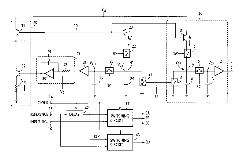
24 Referring now to Fig. 3, there is shown a sample-and-hold phase
2s detector of the present invention which eliminates the need for external26 connections for resistance and capacitance elements. The phase detector
27 of this invention comprises an NPN transistor 32 which is provided in a
28 current setting circuit 40, the collector of transistor 32 being connected to29 the collector of transistor 11 and the emitter thereof being connected to a
30 current setting resistor 13 having the value RB. To the base of transistor 32
.. ,
2075127
s
is connected an integrator 27 formed by a resistor 28, a capacitor 29 and
2 an operational amplifier 30 whose positive input is supplied with a voltage
3 Vc = VCC/2
4 According to the present invention, the transistor 8 acts as a first
5 constant current source. A second constant current source is provided
6 by a PNP transistor 20 whose emitter is connected to voltage supply Vcc
7 and whose base is connected to the bases of both transistors 8 and 11. A
8 current mirror circuit is therefore formed between transistors 20 and 11 in a
9 manner similar to that between transistors 8 and 11. Transistor 20
produces a collector current Ic' corresponding to the current control signal
1 1 on line 10. The collector current Ic' is given by:
12 Ic = IB W20/W1l (7)
13 where, W20 represents the emitter size of transistor 20.
14 The collector of transistor 20 is connected through an analog switch 22to a circuit junction 41, which is grounded by a parallel circuit formed by
16 an analog switch 21 and a storage capacitor 24 with a capacitance value
17 CRI. Circuit junction 41 is further connected by a sampling switch 23 to a18 buffer amplifier 26 whose output is connected to the input of integrator 27.
19 A sampling capacitor 25 is connected to the input of buffer amplifier 26,
which forms a sample-and-hold circuit with capacitor 25 and switch 23.
21 Switches 21 and 23 are driven by pulses SB and SC, respectively.
22 A delay circuit 42 is connected between terminal 15 and switching
23 circuit 17 to produce a delayed reference signal REF' which is delayed by
24 interval TD with respect to reference pulse REF so that, instead of the pulse
SA, switching circuit 17 produces a switching pulse SA' having a duration
2 6 corresponding to the delay time TD-~3 which lasts from the leading edge of an
27 input signal pulse to the leading edge of the delayed reference pulse REF' as28 shown in Fig. 4. In addition, a second switching circuit 43 is connected to
29 receive the delayed reference pulse REF' and the non-delayed reference
3 0 pulse REF to supply a switching pulse SD to switch 22. This switching pulse
207~127
- 6 -
SD is present during the interval from the leading edge of the reference
2 pulse REF and the leading ~edge of the delayed reference pulse REF'.
3 Storage capacitor 24 is charged with the collector current Ic' when4 analog switch 22 is turned on in response to switching pulse SD to develop
s a voltage VCRI which varies linearly with time as shown in Fig. 4 until it
6 reaches the following maximum value Vx:
7 Vx = TD IB W20/(W11 CR ) (8)
8 The voltage developed in storage capacitor 24 is sampled by switch
9 23 in response to a switching pulse SC and stored in capacitor 25 to
produce a sampled voltage Vx' which is coupled through amplifier 26 to
11 integrator 27. The energy stored in capacitor 24 is discharged completely
12 through switch 21 in response to a switching pulse SB.
13 The integrator 27 operates as a differential integrator to produce the
14 following output Vy by integrating the difference between the sampled
voltage Vx' and the reference voltage Vc:
16 Vy = c1 R ¦ (VC - VX)dt (9)
17 where C and R are the values of integrating capacitor 29 and resistor 28,
18 respectively. This differentially integrated voltage Vy drives the base of
19 transistor 32. In this way, the current IB passing through resistor 13 is:
2 0 IB = (VY--VBE)/RB (10)
21 From Equation (8), the following relations hold:
22 IBO = VC W11 CR /(TD W20) (11)
23 IB=IBO+~IB (12)
24 where IBO jS the value of current IB if the sampled voltage Vx' is made equalto reference voltage Vc, and ~IB jS the difference between IB and IBO
2 6 Substituting Equations (1 1 ) and (12) into Equations (9) and (10) and
27 differentiating Equations (9) and (10) result in the following relation:
2 8 d~lB/dt =--~IBII
29 where ~ is a time constant given by Equation (14):
2075127
~ = RB C R- W11 CR/TD W20 (14)
2 Therefore, ~IB jS given 6y Equation (15):
3 ~IB = ~IBO exp (--t/~) (1 S)
4 where ~IBO jS an initial, arbitrary value.
s It is seen that, while ~IB jS of arbitrary value, it eventually converges to
6 zero with the time constant ~ and the current IB automatically adjusts itself
7 through a closed loop feedback operation to the current value IBO given by8 Equation (11). Therefore, the difference between the voltage Vx' and
9 reference voltage Vc is reduced substantially to zero. This indicates thatvariabilities of the value of resistor 13, which would result from the
11 fabrication of resistive materials on LSI chips, are absorbed. The
12 current IB determines the emitter current of transistor 8 and the charging13 current of capacitor 4, and hence it determines the phase-to-voltage conversion
14 coefficient K of the sample-and-hold phase detector 44 formed by
15 transistor 8, switches 5, 6 and 7, capacitors 3 and 4 and amplifier 2. This
1 6 conversion coefficient is derived from Equations (1), (5), (6) and (11) as
1 7 follows:
1 8 K 2~ TD W20 CR (1 6)
19 The timing ratio T/TD can be precisely determined if the delay circuit
42 is implemented with a shift register and the ratios Wg/W20 and CRI/CR
21 can also be determined precisely because transistors 8 and 20 and capacitors 4
22 and 24 are fabricated on the same LSI chip. Therefore, a precision phase-
23 to-voltage conversion coefficient K can be established by the present
24 invention. If transistors 8 and 20, capacitors 4 and 24, and capacitors 3 and
25 are fabricated identically to each other on an LSI chip, Equation (16)
26 can be rewritten as follows:
2 7 K = Vc T/(27~ TD)
28 It is seen from the above description that resistor 13 can be integrated
29 on a common LSI chip with other circuit components, using electrically
2075127
resistive materials or fabricating a transistor circuit that generates a voltage2 corresponding to an input current. Since capacitors 4 and 24 contribute to
3 the determination of the coefficient K as relative values of CR and CRI, their
4 absolute value can be reduced to advantage, allowing integration of these
s capacitors on the same LSI chip. The reduction of capacitor 4 results in a
6 reduction in charging current and hence the power consumption can be
7 reduced.
8 The foregoing description shows only one preferred embodim,ent of
9 the present invention. Various modifications are apparent to those skilled
in the art without departing from the scope of the present invention which
11 is only limited by the appended claims. For example, instead of bipolar
12 transistors, MOS transistors could equally be used as well.