Note : Les descriptions sont présentées dans la langue officielle dans laquelle elles ont été soumises.
1' 2075890
Bach~lo~l~ of the Invention
The present invention relates to amplifiers such as
those employed in AM broadcasting and, more particularly,
to such amplifiers including means for ~ini~i7ing
distortion and noise resulting from variations in the DC
power supply.
It is known that noise and~or other ~ariations
appearing on the output of a DC power supply connected to
the input of an amplifier may result in distortion. The
power supply noise i5 of particular concern in high power
amplifiers, such as those found in transmitters
conventionally used in commercial A~ broadcasting. It is
known to employ large capacitors connected across the power
supply to reduce low freguency AC supply voltage variations
caused by power supply ripple and low frequency transmitter
modulation. These power supply ~ariations may well be
reduced subgtantially by connecting a large amount of
capacitance across the power supply output. Howe~er, such
capacitors employed with high power DC power sources are
207S890
quite large both in volume and in weight. The inclusion of
such capacitors is undesirable from the standpoint of cost,
size iand weight.
It is also known that some AM transmitter circuits
employ a low frequency distortion correction circuit that
takes a sample of the power supply output and then
generates a correction signal that is used to compensate
for power supply sag. Such prior art circuits include, for
example, the U.S. patents to H. I. Swanson et al.,
4,737j731, H. I. Swanson, 4,580,111, and D. H. Covill,
4,605,910. Each of these patents discloses circuitry for
minimizing modulation distortion of an amplitude modulated
RF carrier signal resulting from variations in the DC power
supply. In each case, a feed forward technique is employed
in which a sample of the input DC voltage signal is
obtained and is combined with the input audio signal to
compensate for variations in the magnitude of the DC supply
voltage prior to supplying the input audio signal to the
amplification stages of the transmitter.
In the prior art discussed immediately above, the AC
and DC components of the power supply sample are used for
both long term DC supply changes and short term sags such
as power supply ripple or low frequency transmitter
modulation. In low power transmitters, correction loops
typically treated the AC and DC components equally in terms
of phase and gain of the signals, since large amounts of
supply filter capacitance were practical in most cases.
-~- 207~9~
~owever, with higher power transmitters, such as those
exceeding 50 kilowatts, the cost of such filter capacitance
prohibits their use for minimizing power supply sag.
Moreover, at higher power levels, the transmitters tax the
AC main input lines and may possibly cause additional power
supply sag with modulation. In view of these factors, it
has been found desirable that the AC component of the power
supply sample be separated from the DC component so that
additional gain and phase correction may be made to the AC
component independent of variations in the DC component to
achieve optimum low frequency distortion and minimum AM
noise .
SummarY of the Invention
It therefore a primary object of the present invention
to provide a correction signal wherein the phase and gain
of the AC component of the power supply sample may be
varied independently of the DC component.
In accordance with the present invention, an amplifier
system is provided having improved distortion reduction.
This system includes a DC voltage source having AC and DC
components. An input signal to be amplified is supplied to
an amplifier coupled to a DC voltage source for amplifying
the input signal to provide an output signal in accordance
therewith. Correcti~n signal circuitry is provided and
includes circuitry for separating the AC and DC components
and varying the magnitude and phase of the AC component
independently of the DC component to provide an adjusted AC
_4_ 207~0
component. The DC component and the adjusted AC component
are summed together to provide an adjusted correction
signal which is then combined with the input signal prior
to application of the input signal to the amplifier.
S In accordance with another aspect of the present
invention, the amplifier system is an RF amplifier system
and the amplifier means includes a plurality of actuatable
RF power amplifiers each connected to the DC voltage source
and each, when actuated, for receiving and amplifying an RF
drive signal with each power amplifier having an output
circuit for providing an RF output signal. One or more of
the RF amplifiers are actuated in dependence upon the
magnitude of the input signal. The RF output signals are
then additively combined to provide a combined RF output
signal. The adjusted correction signal and the input
signal are combined prior to actuation of one or more of
the ~F amplifiers.
Brief Description of the Drawinqs
The foregoing and other objects and advantages of the
present invention will become more readily apparent from
the following description as taken in conjunction with the
accompanying drawings, wherein:
Fig. 1 is a schematic-block diagram illustration of
one application to which the present invention may be
2S applied;
Fig. 2 is a prior art schematic circuit illustration
of one of the power amplifiers employed in Fig. 1;
2075890
Fig. 2A is a prior art simplified schematic circuit
useful in understanding the operation of the circuit shown
in Fig. 2;
Fig. 3 i5 a schematic-block diagram of the correction
circuit in accordance with the present invention;
Fig. 4 is a graphical illustration showing phase and
amplitude with respect to frequency useful in describing
the invention herein;
Fig. 5 includes waveforms in Figs. 5A, 5B and SC
showing the operation of circuitry in accordance with the
prior art without the correction circuit of the present
invention; and
Fig. 6 includes waveforms in Figs. 6A, 6B and 6C
showing the operation resulting with the inclusion of the
correction circuitry in accordance with the present
invention.
Description of Preferred ~mbodiment
One application of the present invention is in
con~unction with the use of RF power amplifiers employed in
AM broadcast transmitters. An example of such a
transmitter is presented in Fig. 1 and takes the form of a
digital amplitude modulator such as that illustrated and
described in the aforesaid U.S. Patent No. 4,580,111, which
is assigned to the same assignee as the present invention~
,
, . ~,
-6- 207~9U
The discussion which follows is directed to an
explanation of the operation of the circuitry shown in Fig.
1 followed by a detailed description of a power amplifier
as illustrated in Figs. 2 and 2A herein as background for
S the discussion of the invention presented with respect to
the embodiment illustrated herein in Fig. 3.
Referring now to Fig. 1, the amplitude modulator 10 is
illustrated as receiving an input signal from input source
12 which may be the source of an audio signal. Modulator
10 generates an RF carrier signal which is amplitude
modulated as a function of the amplitude of the input
sign~l from source 12. The amplitude modulated carrier
signal is provided on an output line connected to a load
14, which may take the form of an RF transmitting antenna.
lS A digitizer 16 provides a plurality of digital control
signals Dl through DN which have values which vary in
accordance with the instantaneous level of the input
signal. The control signals are binary signals each having
a binary 1 or a binary 0 level. The number of signals
having binary 1 or binary 0 levels is dependent upon the
instantaneous level of the input signal.
Each of the output control signals Dl-DN is supplied
to one of a plurality of N RF power amplifiers PAl-PAN. The
control signals serve to turn associated power amplifiers
either on or off. Thus, if the control signal has a binary
1 level, then its associated amplifier is inactive and no
signal is provided at its output. However, if the control
-7- 20758~0
signal is o~ a binary 0 level, then the power amplifier is
active and an amplified carrier signal is provided at its
output. Each power amplifier has an input connected to a
single common RF source 20. The RF source 20 serves as the
single source of an RF carrier signal which is supplied by
way of an RF splitter 22 so that each amplifier PAl-PAN
receives a signal of like amplitude and phase and
frequenc~. The carrier signal is amplitude modulated in
accordance with the control signals D1-DN and the amplitude
modulated carrier signals will be of like frequency and
phase. These signals are supplied to a combiner circuit 24
comprised of a plurality of transformers Tl, T2, . ~ TN.
The secondary windings act as an independent signal source,
whereby the signals provided by the various transformers
additively combine with one another to produce a combined
signal which is supplied to the load 14. This combined
signal has the same frequency as the RF signal supplied by
the RF source 20, but the amplitude of the combined signal
is modulated in accordance with the input signal supplied
by the input source 12.
As is conventional in such a system, the RF source 20
includes an RF oscillator 21 having a frequency on the
order of 500 to 1600 KHz. This oscillator feeds an RF
driver 23, the output of which is supplied to the power
amplifiers PAl-PAN. The RF driver provides power
amplification of the RF signal obtained from oscillator 21
prior to the signal being supplied to the power amplifiers
-8- 2075~0
at which modulation also takes place. The RF driver 23 may
include several stages of amplification and may be
configured similar to the power amplifiers PAl-PAN.
Fig. 2 illustrates one form which the power amplifier
PA1 of Fig. 1 may take, the other power amplifiers PA2-PAN
being similar. The power amplifier illustrated includes
four semiconductor amplifier elements 70, 72, 74 and 76
connected in a bridge arrangement across a DC power supply
voltage of, for example, 250 volts. The primary winding 44
of the associated transformer 36 is connected across the
bridge junctions J1 and J2 f the four semiconductor
elements.
More particularly, the semiconductor amplifier
elements are metal oxide semiconductor, field effect
transistors (MOSFETs) having three electrodes,
conventionally identified as the gate, drain, and source.
The drain-source paths of the transistors 70 and 72,
representing their primary current paths, are connected in
series across the DC power supply, as are the drain-source
current paths of transistors 74 and 76. The primary
winding 44 of the corresponding combiner transformer Tl is
connected in series with a DC blocking capacitor 78 across
the common junctions J1 and J2 between transistors 70 and 72
and transistors 74 and 76.
2S The transistors 70, 72, 74 and 76 effectively operate
as switches to connect the tWD sides of the primary winding
44 to either the DC voltage source or to ground. By proper
-9- 207~9~
operation of these transistors, the transformer winding 44
can be connected in either direction across the DC power
supply.
This can perhaps be more readily understood by
reference to Fig. 2A, which is a simplified illustration of
the Fig. 2 circuitry. In Fig. 2A the transistors 70, 72,
74 and 76 are respectively characterized by con~entional
single pole, single throw switches Sl, S2, S3, and S4. As
shown in Fig. 2A, the switch S1 is open and the switch S2 is
closed, whereby the common junction Jl between them is
grounded. The switch S3 is closed and the switch S4 open,
however, whereby the ~unction J2 between those switches is
connected to the DC supply voltage. Current will therefore
pass through the primary winding 44 in the direction
indicated by the arrow 80.
When all four switches Sl-S4 are thrown to their
opposite states, current will pass through the output
winding 44 in the opposite direction. Thus, when switches
S1 and S4 are closed and switches S2 and S3 opened, junction
J1 is connected to the ~C supply and junction J2 is
connected to ground. In this case the current through the
primary winding 44 of the transformer is in a direction
opposite to that indicated by arrow 80 of Fig. 2A. An AC
signal can thus be applied across the coil 44 by cyclically
switching the switches S1-S4 between these two alternate
states. If this is done at RF frequencies, then an RF
carrier signal results.
-10- 2075~90
Referring back to Fig. 2, the transistor switches 70,
72, 74 and 76 are controlled by signals applied to their
gate electrodes. The gate signals for all four transistors
are derived from individual secondary transformer windings.
This transformer has a toroidal ferrite core with a primary
winding 82 and four secondary windings 84, 86, 88 and 90
wound around it. The turns ratio of the transformer is
l:l, whereby the same signal appearing at the primary is
applied to each of the circuits connected to the four
secondary windings.
Each of the four secondary windings is connected
between the gate and source electrodes of an associated one
of the MOSFETs 70-76. The secondary 84 is directly
connected between the gate MOSFET 70 and junction J1~ while
secondary 88 is similarly directly connected between the
gate of MOSFET 74 and junction J2. The secondary windings
86 and 90 are in like manner connected between the gate and
source electrodes of MOSFETS 72 and 76, however in these
cases impedance networks 92 and 94 are connected in series
with the coils 86 and 90, respectively. Each impedance
network 92, 94 includes a parallel combination of a
resistor 96, 98 and capacitor 100, 102. The purpose of
these impedance networks will be described hereinafter
during the description of the amplifier control circuitry
104.
The primary winding 82 of the toroidal transformer is
connected to the output of the RF source 20, which provides
-11- 207~90
a sinusoidal RF driving voltage to the power amplifier.
Each MOSFET turns "on" when the RF signal applied to its
gate is on its positive half cycle and "off" when the
applied signal is on its negative half cycle. The MOSFETs
therefore cyclically turn on and off at a frequency and
phase of the applied RF gate signal. The windings 84 and
90 are connected across MOSFETs 70 and 76 in similar
directions whereby the signals appearing at the gates of
these transistors are in phase with one another. MOSFETs
70 and 76 therefore turn on and off in unison. Windings 86
and 88, on the other hand, are connected across MOSFETs 72
and 14 in a direction opposite to the direction of
connection of the windings 84 and 90. The signals applied
to the gates of MOSFETs 70 and 76 are therefore 180 out of
phase with respect to the signals applied to the gates of
transistors 74 and 72. Consequently, when transistors 70
and 76 are "on", transistors 72 and 74 are "off", and vice
versa.
Due to the nonlinear transfer characteristics of the
MOSFETs 70, 72, 74 and 76, the MOSFETs will abruptly turn
on and off in response to the applied sinusoidal signal,
rather than linearly following it. The signal applied
across the ~unctions Jl and J2 will therefore have
essentially a squarewave form, though at the frequency of
the applied RF input signal. The load 14 to which the
output of the combiner circuit 24 of Fig. 1 is connected
207S890
will generally be frequency selective, and will select only
a fundamental component of this squarewave.
As shown in Fig. 2, the power amplifier PA1 includes a
switching circuit 104 for turning the power amplifier on
and off in response to the control signal appearing on the
digitizer output line D1. The switching circuit 104
includes an NPN bipolar junction transistor 106 having its
emitter grounded and its collector connected to the gates
of MOSFETs 72 and 76 through corresponding diodes 108 and
110. The base of the transistor 106 is connected to the D
output of the digitizer 24 through a base resistor 112.
When~the control signal applied to the base resistor 112
has a high logic level (i.e., logic "1"), base current is
applied to the transistor 106, forcing it into a
saturation. The gates of the transistors 72 and 76 are
then effectively grounded through the corresponding diodes
108 and 110. This has the effect of clamping the gate
signals of these transistors to a ground potential, thereby
forcing both of them to remain in an "off" condition. The
primary winding 44 i~ thus effectively disconnected from
ground, thereby turning off the power amplifier.
The resistors 96 and 98 in the gate circuits of
MOSFETs 72 and 76 limit the DC curren~ through transistor
106 when it is saturated. Were these not included the
current through the transistor 106 would be quite high
because the windings 86 and 90 act as voltage sources. The
capacitors 100 and 102 bypass the resistors, reducing their
2075890
effect at RF frequencies. A third capacitor 114 is
connected between both capacitors 100 and 102. This
capacitor improves the turn-on/turn-off characteristics of
the amplifier.
When the control signal applied to the base of
transistor 106 is at a low logic level (i.e. logic "0"),
the transistor 106 is cut off and the operation of the
amplifier 26 is substantially as described previously.
However, this logic 0 signal is a negative signal and it
serves to turn on PNP transistors 95 and 97 through base
drive resistors 91 and 93, respectively. When these
transistors are turned on forcing them into saturation,
they, in turn, rapidly drive the MOSFET switching
transistors 72 and 76 into saturation.
The turn on control signal applied to transistors 95
and 97 must be sufficient to drive these transistors into
saturation so that the MOSFET switching transistors operate
as switches and not resistors which could cause excessive
MOSFET dissipation, high stress and potential failure.
This turn on or binary "0" signal is a negative DC voltage.
The modulating audio input signal 12 is supplied to an
analog processing circuit 33 which adds a DC level to the
audio signal and provides this audio plus DC level to a DC
regulator 35 which supplies regulated DC voltage to a
digieizer 16. The outpu~ of the analog processing circuit
33 is also supplied to an analog divider circuit 39 which
divides the audio frequency signal by a sample voltage V1
2075890
and which is a sample of the power supply DC voltage VDC.
The audio frequency signal divided by the sample voltage V
is supplied to an analog-to-digital converter 37. The
converter 37 converts the signals into a digital
representation thereof and which may be internally decoded
to provide a number of control signals Dl-DN. The number
of the control signals that are supplied by digitizer 16
will vary with the magnitude of the audio signal and DC
level received from the audio input. The digitizer
supplies either a binary 1 (turn off signal) or binary 0
(turn on signal) to the respective power amplifiers PA1-PAN.
The operation is otherwise as described hereinbefore.
The sample signal V1 that is supplied to the divider
39 is illustrated in Fig. 1 as being obtained from a
correction circuit 41 having its input taken from the
midpoint of a voltage divider made up of series connected
resistors 43 and 45. This voltage divider is connected
across the output of a suitable power supply circuit such
as a three phase rectifier 17 connected across a line
voltage source 19. It is conventional with such power
supplies to have a capacitor C connected across the power
supply with the capacitor having a value on the order of
0.5 farads. The DC voltage VDC may be on the order of 230
volts.
~The prior art distortion correction circuits
identiied hereinbefore obtained the sample voltage V
directly from the voltage divider and not by way of a
-15-
2075890
correction circuit, such as circuit 41 in Fig. 1.
Attention is now directed to a more detailed description of
the correction circuit presented with respect to Fig. 3 and
the waveforms of Figs. 4, 5 and 6.
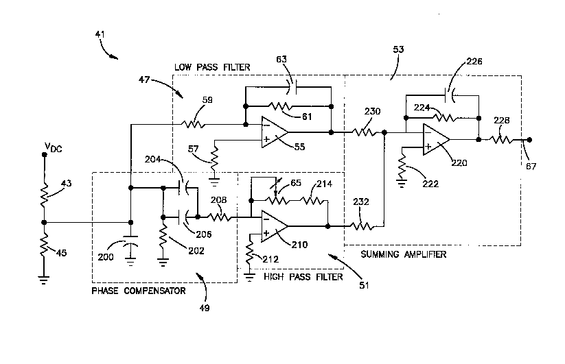
The correction circuit 41 as depicted in Fig. 3
receives a sample voltage from the voltage divider
comprised of resistors 43 and 45 with the sample voltage
having a value on the order of approximately 10 volts DC.
This sample voltage is supplied to a low-pass filter 47
which serves to predominantly pass the DC component of the
sample voltage. The sample voltage is also supplied to a
phase compensator 49 and then to a high pass filter 51
which removes the DC component and passes only the AC
component ~f the sampled voltage. As will be brought out
hereinafter, the AC component is phase changed by the
compensator 49 and its gain is changed with an adjustable
potentiometer 65 in the high pass filter. The AC and DC
components are then summed together in a summing circuit 53
to provide an adjusted correction signal at the output
circuit 67 of the summing circuit which is then applied as
the correction signal V1 to the divider 39 described
hereinbefore.
The low-pass filter 47 is a 2 Hz active low-pass
filter that serves to predomin~ntly pass the DC component
of the sample voltage. The filter 47 employs an amplifier
55 having its positive or noninverting input connected to
ground by way of a xesistor 57. The negative input of the
~ -16-
2075890
amplifier i5 connected to the junction of resistors 43 and
45 to obtain the sample voltage therefrom by way of input
resistor S9. As is conventional, the low-pass filter
includes a resistor 61 and a capacitor 63 connected
together in parallel between the output of the amplifier
and the negative input. This is a first order low-pass
filter and with the components employed may exhibit a gain
on the order of 0.36 in the pass band.
As is shown in Fig. 3, the phase compensator 49
includes an RF bypass capacitor 200 connected in parallel
with a resistor 202 across the resistor 45. Capacitors 204
and 206 are connected together in parallel and extend from
the junction of capacitor 200 and resistor 202 and thence
in series with a resistor 208 to the high pass filter 51.
The capacitors 204 and 206 together with the resistor 208
are the primary components for providing phase change. The
phase change caused by the phase compensator 49 is to
correct for the change in phase that takes place in the AC
component of the power supply voltage VDC between the output
of the three phase rectifier 47 and the amplitude modulated
output of the transmitter.
The high pass filter 51 is a single order high pass
filter and with the c~mponents employed exhibits a variable
gain in the pass band of 0.13 to 0.4~. The three db cuto~f
frequency for this example is about 2 Hz. The filter 51
includes an amplifier 210 having its positive or
noninverting input connected to ground by way of a resistor
2075890
212. The feedback path between output and the negative
input includes potentiometer 65 connected in series with a
fixed resistor 214. As the resistance of potentiometer 65
is increased, the gain will increase to increase the
magnitude of the AC component passed by the filter 51.
The summing amplifier ~3 includes an amplifier 220
having its positive or noninverting input connected to
ground by way o a resistor 222. A resistor 224 and a
capacitor 226 are connected together in parallel between
the output and negative input of the amplifier 220 as is
conventional. The output from the summing amplifier is
taken at output circuit 67 connected by way of a resistor
228 to the output of amplifier 220. The outputs of filters
47 and 51 are applied through resistors 230 and 232,
respectively, to the negative input of amplifier 220 in the
summlng amplifier circuit 53. The summing amplifier
provides unity gain for each of these inputs. The
resultant output at output circuit 67 is on the order of
3.6 volts ~C for the 10 volt input.
Reference is now made to Fig. 4 which shows the phase
response and the amplitude response at output circuit 67 in
Fig. 3. The phase response is illustrated by curve 300 and
the ampli~ude response is illustrated by curve 302. The
phase response curve 300 shows the phase angle in degrees
with~respect to frequency from 10 Hz to 1 kHz. The
amplitude response is given in db over a frequency range
from lO Hz to 1 kHz. This presents test results of an
207ssso
actlve correction circuit showing phase and amplitude
response of the circuit of Fig. 3 that is required to
provide optimum performance at 100 kilowatts of operation
over a frequency range from 10 Hz to 1 kHz. The phase
response curve 300 shows that -50 phase shift is reguired
at 100 Hz to compensate for power supply sag when the power
amplifiers are operating at 100 kilowatts. Similarly, the
amplitude response curve 302 shows that a 5 db gain is
required at 20 Hz to correctly compensate for power supply
sag when operating at 100 kilowatts. These adjustments are
provided by the circuitry of Fig. 3.
Reference is now made to waveforms in Figs. 5A, 5B and
5C. The waveform of Fig. 5A represents the RF envelope of
the RF output signal taken from transmitter at the load 14
of Fig. 1. Fig. 5B illustrates the AC component of the
power supply voltage VDC which shows that a phase shift
takes place between the input and the output and this may,
for example, be on the order of 10. If a correction
signal is provided in accordance with the prior art
referred to hereinabove (which does not include the
correction circuit 41) then the correction signal as shown
in the waveform of Fig. 5C will be of the same phase as the
power supply voltage VDC and, hence, will not result in a
proper correction for this phase shift.
The waveforms in Figs. 6A and 6B correspond with those
in Figs. 5A and 5B. However, the waveform in Fig. 6C
represents a correction signal provided in accordance with
~ _~9_
20758S0
the present invention by employing the correction circuit
41 of Fig. 3. This provides a phase shift for the
correction signal. More specifically, this shows the
lagging phase shift in the power supply is phase corrected
by the correction circuit of the invention herein to allow
the signal to the analog divider 39 to be the proper phase
and amplitude for minimum distortion.
Although the invention has been described with respect
to a preferred embodiment, it is to be appreciated that
various modifications may be made without departing from
the spirit and scope of the invention as defined in the
appended claims.