Note : Les descriptions sont présentées dans la langue officielle dans laquelle elles ont été soumises.
2076421
-0287
TITLE
Method for Mal~ng Thlck Film/Solder Jolnts
Field o~;Lç~ption
The invention ls dlrected to a method for making
thick film/solder loints and, in particular, it is dlrected to such a
0 method which will produce thick film/solder ~oints which have
good thermal cycled adhesion.
Backg~nd of thelly~on
The current trend in the microelectronics industry
is to surface mount integrated clrcuits and other components
onto thick fllm metallized substrates. Although this is a cost
e~ective interconnection and packaging method which lends
20 itself to mass prcduction, certain reliability problems have been
encountered in trying to implement its approach. Soldering,
which is the preferred method for attaching leads and IC
packages, can lead to solder ~oint failures-particularly on thern1al
cycling. This has severely limlted the use of thick films for
2s .certain applications such as automotive electronics and some
military and high power applications where good thermal cycled
perrormance is essential.
The engine compartment of an automobile is a
30 particularly severe environment where circuits encounter
temperatures of 150C during normal operation and excursions
to 160 to 170C for short times after the engine is stopped.
Conversely, in some areas, the ambient temperature can drop to
-50C. Although the above temperatures represent extreme
35 conditions, the circuit must be able to wlthstand a significant
number of thermal cycles in this temperatures range without
appreciable degradation in adhesion to avoid to catastrophic
2~764~1
-0287
-- 2 --
failure. Thls abllity to wlthstand thermal cycllng condltlons, I.e.,
thermal cycled adhesion (T(:A), Is becoming even more
Important because of the longer warranty perlods that are now
belng orrered by automoblle manufacturers.
Conventional Ag/Pd thick film conductors soldered
wlth Sn/Pb eutectic solder exhibit relatively poor thermal cycled
adhesion. Sn/Pb solders have a much higher thermal coemcient
of expansion (TCE) than the alumina substrate and thick film
0 conductor. This mismatch in TCE results in high tensile
stresses in Sn/Pb solder joints made to thick fllm conductors.
Although surface mount technology (SMT) is an
attractive assembly method for high density electronic systems,
5 there are still problems which must be solved. LCC, MLC, and
other chip components are generally attached to alumina or
ceramic multilayer interconnect boards via reflow of Sn/Pb
solder paste. Since a large TCE mismatch exists between the
substrate, metalliza~ion and solder, it is apparent that a tensile
20 strain will be induced into the thick film at the base of the
solder fillet. For the case of a soldered copper thick film on an
alumina substrate, the strain E due to the TCE mismatch can be
estimated as rollows:
For soldered Cu film thermally cycled between
-50 and +150C
T
= t25-6)(200)=3800 ppm
The tensile stress in the copper fllm, ~cu, can be
estimated from Hookes law:
~cu = E
where E is Young's modulus of Elastlcity
L 0287
For thermal cycling between -50 and ~150C, the
tensile stress is estlmated to be:
~cu= 3800 x 10-6-3x106 = 11,400 psi (tenslon).
This calculat~on is only approximate because aCU (thlck fllm) Is
5 less than aCu (bulk) and some of the tenslle stress will be
relleved by plastic flow In the solder and copper. More accurate
estimates of stresses in SMT solder Jolnts have been made by
the Fillite Element Methcd (FEM) of analysis. The FEM results
indlcate tensile stresses of the same order of magnitude.
0 Obviously, the presence of an LCC or IC chip rurther complicates
the stress situation.
The important point is that tensile stresses due to
TCE mismatch are considerable and any cracks which develop
5 and propagate in the thick film conductor, dielectric, or IC
chips can result in open circuit failures.
In addition to stresses caused by large differences in
TCE, thick film solder pads are subjected to a number of
20 mechanical and chemical interactlons on thermal cycling which
degrade adhesion, namely:
Tin diffusion from the solder into the film with the
formation and growth of intermetallic compounds.
25 Formation of a weak, Pb-rich zone in the solder.
High strains due to the large TCE mismatch between
solder fillet and film/substrate.
Creep related processes including coalescence of
microvoids and oxidation of the solder.
30 Crack propagation through the solder/conductor to the
substrate/dielectric Interface.
~ pical data for thermal cycled adhesion degradaUon
of soldered thick film conductors are shown in ~igure 1. All the
2076421
L -0287
curves exhiblt a small Inltlal drop in adheslon upon thermal
cycllng, followed by a rapld decllne atter extended cycllng.
Summarv of the Inventlon
In a flrst aspect, the inventlon is directed to a
method for making thlck film/solder ~olnts havlng a preselected
area comprlsing the sequentiai steps of
( 1 ) applying to an electrically non-conductive substrate a
patterned layer having a preselected solder pad area of a
flrst thick fllm conductive composition comprising finely
divided particles of (a) 85.0-98.5% wt. of a pure unalloyed
conductive metal or low alloy thereof selected from ~u, Ag
and Cu having a particle size of 0.5-5 microns, (b) 1-10%
wt. glass rrit, and (c) 0.5 to 5.0% wt. spinel-formîng metal
oxide, all of (a), (b) and (c) being dispersed in organic
medium;
(2) firing the first thick film conductive composition layer to
effect volatilization of the organic medium therefrom and
liquid phase sintering of the inorganic binder;
25 ~3) applying over only the solder pad area of the fired first
thick fllm conductive layer a layer of second thick film
conductor composition comprlslng (a) 94.0-99.3% wt.
pure unalloyed conductive metal or low alloy of a metal
selected from Au, Ag, and Cu having a particle size of 0.5-
10 microns, (b) 0.2-1.0% wt. glass frlt, and (c) 0.5-5.0%
wt. splnel-formlng metal oxide, all of (a), (b) and (c) being
dispersed in organic medium;
2076421
E L ~287
-- 5 --
(4) flring the second thick fllm conductive layer to efÇect
volatillzat~on of the organlc medium therefrom an~ llquid
phase sintering of the inorgan~c blnder; and
5 (5) forming the solder~oint by applylng to the solder pad area
of the fired second thlck fllm conducUve layer a layer of
sort, low-Sn solder havlng a melting polnt of 120-300C.
In a second aspect, the invention is dlrected to a
0 method for making a thick film/solder Joint having a preselected
area comprising tl1e sequential steps of:
( 1 ) applying to an electrically non-conductive substrate a
patterned layer having a preselected solder pad area of a
thick film conductive composition comprising finely
divided particles of (a) 85.0-98.5 % wt. of a pure unalloyed
conduct~ve metal or low alloy thereof selected from Au, Ag
and Cu having a particle size Of 0.5-5 microns, (b) 1-10%
wt. glass frit, and (c) 0.5-5.0 % wt. spinel-forming metal
oxide, all of (a), (b) and (c) being dispersed in organic
medium;
(2) firing the thick fllm conductive composltion layer to effect
volatillzation oi the organic medium therefrom and liquid
phase sintering of the inorganic binder;
(3) applying over the exposed areas of the substrate
circumscribing the solder pad area and to the outer edges
of the thick fllm conductor within the solder pad area a
thick film dielectric composition comprlslng finely
divided parUcles of glass dispersed in organic medium;
(4) flring the thick film dielectric composition to effect
volatilization of the organic medium therefrom and
sintering of the glass therein; and
2076421
k.~-0287
-- 6 --
(5) rorrning the solder JQlnt by applylng to the surface of the
thlck fllm conductive composiUoll which remains exposed
on the solder pad area a layer of soft solder having a
melting point of 120-300C.
Brlef Descrlption of the Drawing
0 The Drawing consists of six flgures as follows:
Figure 1 is a graphical correlation of adhesion as a
function of the number of thermal cycles for a variety of thick
film materials;
Figure 2 is a graphical representation of three
thermal cycle profiles which were used in the evaluation of the
invention;
Figure 3 is a graphical correlation of adhesion as a
function of aging time showing the effect of fired fllm thickness
of the conductor;
Figure 4 is a graphic correlation of thick fllm
conductor adhesion with aging at various temperatures;
FYgure 5 is a schematic representation of the steps of
the invention which are requlred to make a soldered thick fllm
conductor element; and
Figure 6 is a drawing of the adhesion test bond
conflguration.
2~76421
E ~287
-- 7 --
Flgure 7 is a schematic cross sectional
representation comparlng the conflgurations of the standard and
modifled peel tests.
De~ailed DescrlE~tion of the lnvention
A In_General
0 The performance of thick film conductors sul~ected
to thermal cycle tests can be improved by controlllng several
materials, process and design factors. For example, pure,
ductile thick films with low glass blnder content such as Ag or
Cu exhibit higher thermal cycled adhesion than Ag/Pd alloy
conductors. Likewise, thick, dense films exhibit greater thermal
cycled adhesion than thin, porous films because it takes longer
for tin diffusion from the solder to penetrate through the thick,
dense film.
Solder composition and soldering conditions also
play an important role. Thick fllms soldered with low yield
strength, low-Sn or Sn-free solders perform better in thermal
cycling because some stress relief occurs due to plastic
deformation in the solder. Also, embrittlement of the thick film
due to MxSny intermetallic formation is reduced because of the
lower tin content.
Sometimes on thermal cycling, fatigue failure of the
solder.~oint occurs instead of failure at the thick film/substrate
interface. This can be minimized by producing fine-grained,
void-free solder Joints and by employing solder composilions
which have high fatigue strength. The Coffin-Manson equation ~s
useful in comparing the fatigue strength of solders thermally
cycled under various conditions.
2076421
.,-0287
-- 8 --
Nfa ~Ep = Constant
Follow~ng is a 11st of ractors whlch affect thermal
cycled adhes~on of thlck hlm conductors. By controlllng a
5 combination of these factors, the performance of thlck fllm
materials on thermal cycling can be signlhcantly improved.
~ Metallurgy
Thick film compositions of pure metals such as Ag,
Cu, and Au or low alloys of these metals perform better on
thermal cycling than hard, brlttle alloys like 30/70 Pd/Ag. Pure
metals and their low alloys are softer (low modulus) and
5 therefore can relieve thermal cycling stresses by plastic flow.
Furthermore, thick fllm Ag, Cu, and Au densify on flring without
requlring large amounts of glass binder which makes the fihn
brittle. Stress relief by plastic deformation inhibits crack
propagation and results in higher thermal cycled adhesion.
As used herein, the term "low alloy" means that the
prlmary conductive metal contains no more than 5% by weight
of secondary alloying metal such as a 95/5 Ag/Pd alloy.
C Fired Film Thlckness
As shown by the data presented graphically in
Figure 3, the use Or thicker flred films improves aged adhesion.
If suMcient thickness cannot be obtained in a single printing
30 and firing operation, several conductor layers can be applied by
sequential printing and firing or by cof~ring two or more layers.
Standard thick fllm conductors are deslgned to have
good solderability and adhesion when hred on 96% alumina
35 substrates or over dielectric. When two layers of a conductor are
2076~21
~L-0287
_ g _
built up by sequential firing, the top layer often wlll not have
adequate solderablllty. This dlmculty can be overcome by uslng a
dlffererlt composltlon for the top layer which contains less rrlt
than the standard conductor deslgned for flring on ceramlc.
5 Therefore for optlmum overall performance, multiple layer thick
fllms may require different composltions for the bottom and top
layers--particularly if the layers are sequentially flred rather
than coflred.
0 In general, the flrst layer on the ceramic should be a
thick film conductor with good TCA (dense, pure or low alloy
metal film with mLxed bonding) and the top layer should be a
conductor with good aged adhesion (i.e., low frit and resislance
to leaching and degradation by tin solders). Therefore a thick
film conductor consisting of two layers of optimum composition
will exhibit superior aged and thermal cycled adhesion to either
single layer alone. More particularly, the first conductive thick
filn~ layer should contain 1-15% wt. mixed o~de/frit inorganic
.binder. At least 1% wt. inorganic binder is needed to get
adequate particle bonding. However, more than 15% wt. is
likely adversely to affect TC~. On the other hand, the second
lower frit conductive thick film layer should contain 0.7-6.0%
wt. inorganic binder. At least 0.7% wt. inorganic binder is
needed to get adequate bonding to the underlying thick film
conductive layer, but more than 6.0% inorganic binder is likely
adversely to affect solderabllity of the layer.
It should be mentioned that coflrlng of more than
one or two layers of Cu in nitrogen can lead to organlc burnout
problems and therefore Is not preferred in the practice of the
invention.
2076421
E J287
-- 10 --
D. Composlte /Gradient Thick Fllms
The above sectlon dlscussed the beneflts of using
two or more layers of conductor of dlfferent composltion but the
same metallurgy, I.e., Ag or Cu or Au. Improved performance can
result from using two dlfferent metallurgies, e.g., Ag and Cu and
two dlfferent firing profiles.
For example, Du Pont 6160 Ag has excellent thermal
0 cycled adhesion but poor solder leach and migration resistance
and marginal long-term aged adheslon. By overprinting 6160 Ag
flred in air at 850C with a Cu t~ick film paste (QSl90) fired in
nitrogen at 600C, a composite conductor is obtained which has
the following advantages:
High conductivity
Excellent solderability
Good solder leach resistance
Resistance to rnigration
High aged adhesion
High thermal cycled adhesion
~ Low cost
The overprint Cu must be flred in nltrogen below the Ag-Cu
eutectic temperature of 780C to avoid melting. However, the
composite Ag-Cu thick film exhibits a combination of properties
which cannot be achieved from Ag or Cu alone.
E. Edge Encapsulation
In the course of the studles on which the invention
is based, it has been found that both AA and TCA of the copper
conductive layers can be enhanced by edge encapsulation. By
"edge encapsulation", it Is meant that a fired layer of dielectric
composition is applied over the outer edges of the fired thick
2076~21
~ 0287
-- 11 --
fllm conductor and the exposed areas of the substrate
surroundlng the solder pad.
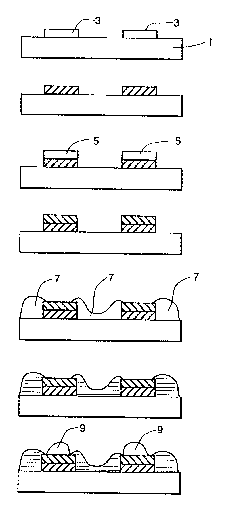
Turning now to Flgure 5 of the Drawing, It consists
5 of seven figures (5a through 5g) whlch illustrate both the
overprinting of Ulick fllm conductive layers and edge
encapsulation to improve the AA and TCA of thlck film
eonductive layers.
0 As shown in Figure Sa, a first thick film conductive
layer 3 is applied by screen printing onto an alumina substrate 1.
Upon completion of drying the paste, the layer 3 is fired at 800-
950C to effect volatilization of the remaining organic medium in
the paste and to sinter the inorganic blnder (Figure 5b). A
second layer of thick film conductive paste 5 is then printed
over the fired layer 3 and dried (Figure 5c). After drying, the
second thick film conductive layer 5 is flred to effect
volatilization of the organic medium in the paste and to sinter
the inorganic binder (Figure 5d). A layer of dielectric thiclc film
paste 7 is then applied over the exposed areas of the substrate 1
and the edges of the top fired conductive layer 5 (Figure 5e) and
the dielectric layer 7 is fired to effect volatilization of the
organic medium and sintering of the dielectrlc solids (Figure 5n.
Soldering is then accomplished by applying molten solder 9 to
the exposed areas of the top conductive layer 5 and cooling the
solder to room temperature (Figure 5g).
F. Barrier Lavers
Poor TCA performance is caused by high stresses
due to TCE mismatch which are superimposed on the aging aI1d
interaction mechanisms as discussed hereinabove. These
stresses can be reduced by using low modulus, high fatigue
207642~
~)287
-- 12 --
strength solders. Another approach Is tu use a barrier layer to
inhibit solder/thlck fllm interactlons which degrade TCA.
The main purpose of the barrier layer Is to prevent
5 Sn difrusion into the fllm and the attendant formation Or a weak,
Pb-rich zone in the solder loint. Nickel is an effective dlfrusio
barrier because NixSny Intermetallics grow at a very slow rate.
However electroless and electrolytic processes must be carefully
selected to prevent destruction of the glass/oxide thick film
0 bond by acidic plating solutions.
R. Keusseyan in copending allowed U.S. Patent
Application S.N. 07/508,871 flled April 12, 1990 and
W. Nebe et al. in copending U.S. Patent Application S.N.
5 07/508,769 flled April 12, l990 disclose the use of thick film
compositions as barrier layers to enable soldering or brazing of
connectors to thick film conductor layers.
G. Solder Com~ _esign
Solder Composition: It is possible to reduce stresses
in the solder joint and to inhibit some of the unwanted reactions
listed above by avoiding the use of Sn-bearing solders. For
25 example, the use of Sn-free solders prevents the formation of
intermetallic compounds which degrade adhesion. As shown in
subsequent examples, copper thick fllms soldered with 50
In/50 Pb solders have excellent aged and thermal cycled
adhesion. Likewise, low-Sn or Sn-free solders will
30 minimize/eliminate in diffusion of Sn from the solder (into the
thick film and wire) which causes a weak, Pb-rich zone in the
solder ~oint. This often results ln type-B failures in the solder
joint after prolonged aging or thermal cycling. (See Section I~
below.)
3S
207~42~
EL-v )87
-- 13 --
The high cost of Indium solders has restricted lts
use for many appllcaUons. However, lt ls clear that eutectlc
Sn/Pb solders are derinltely ~ the optimum composi~on for
applications that requlre good thermal cycled performance.
Effect of Solder Jolnt Characteristlcs on Thermal
Cycled Adheslon: Low yleld strength soft solders (e.g. In and Pb
base alloys) are able to wlthstand thermal cycling better than
higher yield strength Sn/Pb eutectlc solders because some
10 stress relief occurs due to plastic deformation in the solder.
Furthermore, because of their low modulus, the stresses
developed on thermal cycling to low temperatures ls lower tha
with high yield strength solder alloys.
Another important conslderation is the integrity of
the solder joint. For best thermal cycled performance, soldering
conditions should be controlled to produce fine-grained, void-
free solder joint. Furthermore, solder ~oint designs which
minimize plastic strain, ~p, in the solder will reduce fatigue
cracking of the solder joint.
Fine Grain, Void-Free Solder Joints: Conventional
Sn/Pb solders shrink about 4% in volume upon solidi~ication.
This causes voids to develop in the solder ~oint. These voids
2s increase in size and number when tin dirfuses from the solder
into the conductor to form intermetalllc compounds. ~loids also
develop and grow by creep related mechanisms durlng elevated
temperature aging andtor thermal cycling of the solder joint. As
a result, failure eventually occurs in the weak, tin-depleted zone
of the solder Joint.
Fine grains are stronger and resist grain boundary
sliding better than coarse grains. Therefore, for improved
thermal cycled performance, soldering conditions should be
used which develop a flne, uniform grain structure in the solder
207~421
,-0287
-- 14 --
Joint. Reflow soldering 1n conveyor belt furnaces with slow
coollng through the sol~dlflcatlon temperature range promotcs
grain growth and ~hersfore should be avoided. Solderlng
processes whlch Involve rapld solldlflcatlon wlthout solder nux
5 entrapment and gas evolution to yleld dense, fine-gralned solder
~olnts are preferred for appllcatlons whlch requlre hlgh thermal
cycled adheslon.
0 H. Inorganic Binder
The Inorganic binder for the thick film conductor
paste must be a low softening point glass having a dilatometer
softening point o~ 300-800C. In particular, the softening pOillt
5 of the glass should be such that it causes liquid phase sintering,
i.e., it begins to flow, before the conductive metal component
undergoes sintering and densification during cofiring.
A vwide range of glass composltions can be used as
20 the inorganic blnder of the thick fllm conductor so long as the
above-mentioned criteria are fulfilled. In particular, arnorphous
silicates, borosillcates and borates of lead and bismuth have been
found to be particularly suiLable in combination with up to 50%
by weight glass modifiers sueh as alka-ii metal oxides, alkaline
25 earth metal oxides and transition metal oxlde. Mixtures and
precursors of these components may be used as well.
Optlonaily, the binder component may also
containing supplemental fluxing agents such as Bi2O3 and PbO.
I. Spinel-Forming Metal Oxides
It is preferred that the conductive layer atop the
substrate contain a spinel-forming divalent metal oxide for the
35 purpose of improving further the adhesion of the conductive
2076~2~
- ,87
-- 15 --
layer to the substrate. At least 0.5% wt. of the splnel-former
should be used to have any observable technical effect and
preferably at least 1.0% wt. In any event, the amount of splnel-
forming metal oxide should be sufficient to react wlth the Al2O3
5 at the Al203/thick fllm interface. On the other hand, It is
preferred to use not more than 5.0% wt. spinel-forming oxldes
so as not to adversely affect the solderabillty of the conductive
layer.
0 As used herein, the term "spinel-forming metal
oxide" refers to divalent metal oxides which, under the firing
conditions of the invention, are capable of forming spinels
(MeA1204) by reacUon with an underlying alumina substrate.
While the exact mechanism by which these metal oxides
function is not known, it is believed that the metal oxides are
transported through the glass phase to the ceramic substrate
where they interact with the surface of the Al2O3 substrate to
form a mechanically strong splnel structure.
Suitable inorganic oxides are those based upon Zn2+,
Mg2+, Co2+, Cu+2, Ni2+, Fe2+ and Mn2+ ions. Precursors of the
metal oxicles, such as carbonates and oxalates which will
decompose under firing conditions to form the corresponding
metal oxides, may be used with comparable effectiveness.
J. Organic Medium
The inorganic particles are mixed with an essentially
inert liquid medium (vehicle) by mechanlcal mixing (e.g., 0ll a
roll mill) to form a pastelike composition having suitable
consistency and rheology for screen printing. The latter is
printed as a "thick film" on conventional dielectric substrates in
the conventional manner.
2~76~21
EL^ ,87
-- 16 --
Any inert llquid may be used as the vehlcle, Varlous
organic liquids, wIth or without thlcken~ng and/or stabilizl]lg
agents and/or other common addltives, may be used as the
vehicle. Exemplary of organ~c llquids whlch can be used are the
5 aliphatlc alcohols, esters of such alcohols, for example, acetates
and proplonates, terpenes such as plne oll, terplneol and the
like, solut~ons of reslns such as the polymethacrylates of lower
alcohols and solutions of ethyl cellulose In solvents such as pine
oll and the monobutyl ether of ethylene glycol monoacetate. A
0 preferred vehicle is based on ethyl cellulose and beta-terpineol.
The vehicle may contain volatile liquids to promote fast setting
after application to the substrate.
The ratio of vehlcle to solids in the dispersions can
5 vary considerably and depends upon the manner in which the
dispersion is to be applied and the klnd of vehicle used.
Normally to achieve good coverage, the dispersions will contain
complementally 60-90% solids and 40-10% vehicle. The
compositions of the present invention may, of course, be
20 modified by the addition of other materials which do not afrect
its beneficial characteristlcs. Such formulation is well within the
skill of the art.
The pastes are conveniently prepared on a three-roll
25 mill. l'he viscosity of the pastes is typically within the following
ranges when measured on a Brookfleld HBT viscometer at low,
moderate and high shear rates:
2V76~21
EL J287
-- 17 --
Shear Rate (sec-l) Viscosity (Pa.s)
.Z 1 00-5000
300-2000 Preferred
600-1500 Most Preferred
4 40-400
100-250 Preferred
140-200 Most Preferred
384 7-40
1 0-25 Preferred
12-18 Most Preferred
5 llhe amount of vehicle utilized is determined by the final desired
formulation viscosity.
K Formulatio~n
In the preparation of the compositions of the
present invention, the particulate inorganic solids are mixed
with the organic carrier and dispersed with suitable equipment.
such as a three-roll mill, to form a suspension, resulting in a
2s composition for which the viscosity will be in the range of about
100-200 pascal-seconds at a shear rate of 4 sec-l.
In the examples which follow, the formulation was
carried out in the following manner:
The ingredients of the paste, minus about 5%
organic components equivalent to about 5% wt., are weighed
together in a container. The components are then vigorously
mixed to form a uniform blend; then the blend is passed through
3s dispersing equipment, such as a three-roll mill, to achieve a
good dispersion of partlcles. A Hegman gauge is used to
determine the state of dispersion of the particles in the paste.
This instrument consists of a channel in a block of steel that is
2076~2~
EL 287
-- 18 --
25 ~lm deep (1 mil) on one end and ramps up to 0" depth at the
other end. A blade Is used to draw down paste along the lenglll
of the channel. Scratches will appear In the channel where the
agglomerates' dlameter Is greater than the chalmel depth. A
5 satisfactory disperslon will glve a fourth scratch polnt of 10-18
typlcally. The polnt at whlch half of the channel is uncovered
wlth a well dispersed paste is between 3 and 8 typlcally. Fourth
scratch measurement of ~20 llm and "haif-channel"
measurements of >10 ilm Indlcate a poorly dispersed
o suspension.
The remaining 5% consistlng of organic components
of the paste is then added, and the resin content is adjusted to
bring the viscosity when rully formulated to between 100 and
5 200 Pa.s at a shear rate of 4 sec-l. The composition is then
applied to a substrate, such as alumina ceramic, usually by the
process of screen printing, to a wet thlckness of about 30-80
microns, preferably 35-70 microns, and most preferably 40-50
microns. The electrode compositions of this invention can be
20 printed onto the substrates either by using an automatic printer
or a hand printer in the conventional manner, preferably
automatic screen stencil techniques are employed using a 200-
to 325-mesh screen. The printed pattern is then dried at below
200C, about 150C, for about 5-15 minutes before firing. Firing
25 to effect sintering of both the inorganic binder and the fine]y
divided particles of metal Is preferably done in a well ventilaled
belt conveyor furnace with a temperature profile that will allow
burnout of the organic matter at about 300-600C, a period of
maximum temperature of about 700-lOOOC lasting about 5-15
30 minutes, followed by a controlled cooldown cycle to prevent over
sintering, unwanted chemical reactions at intermediate
temperatures or substrate fracture which can occur from too
rapid cooldown. The overall flring procedure will preferal~ly
extend over a period of about 1 hour, with 20-25 minutes to
35 reach the hring temperature, about 10 minutes at the hrirlg
2~7~4~1
EL 87
temperature and about 20-25 mlnutes in cooldown. In some
instances, total cycle times as short as 30 mlnutes can be used,
s I~ T~st Pr~ures
Solderabllity: The solderability tests were
performed as follows: The flred parts were dlpped in a mildly
active rosin flux such as Alpha 611, then heated for 3 seconds by
0 dippping the edge of the ceramlc chlp In the molten solder.
The chip was then submerged in the solder for 10 seconds,
withdrawn, cleaned and inspected. Solderabillty was
determined by the percentage of solder coverage (buildup)
obtained on the thick film test pattern.
Adhesion: The adheslon was measured using an
"Instron pull tester in a 90 peel conflguration at a pull rate of
2 inches per minute. l`wenty gauge pre-tinned wires were
attached to 80 mil x 80 mil pads by solder dipping for 10
20 seconds in 62 Sn/36 Pb/2 Ag solder at 220C or in 60 Sn/40 Pb
solder at 230C using Alpha 611 flux. (Alpha 611 is a tradename
for solder flux made by Alpha Metals Inc., Jersey City, NJ.)
Aging studies were carried out in air in a Blue M Stabil-Therm~
oven controlled at 150C. After aglng, test parts were allowed to
25 equilibrate several hours in air before the wires were pulled. A
peel force of at least 15 newtons after 1000 hours aging at
150C. is considered to be essential ~or most applications.
The standard configuration of the Du Pont "peel"
30 adhesion test is shown in Figure 6. The only difference in the
modifled peel test is that the thin edges of the thick film are
encapsulated with a dielectric. Therefore, the full thickness of
the conductor resists shear failure due to high tensile stresses at
the base of the solder flllet, leading to improved TCA. Solder
3s .~oint failures can be characterized as follows:
2076~21
EL-(, J7
-- 20 --
l~ype A. Conductor/substrate lnterÇace failure (pad lift-ori~;
l~pe B. Conductor/solder failure;
l~pe C. Wire pull out from solder; and
l~ype D. Substrate failure (divoting).
Thermal Cycled Adhesion (TCA): The TCA test
employs the same adhesion (peel) test described ln L above.
However, instead of measuring adhesion after isothermal aging
at 150C, the sample is tested after thermal cycling between two
o temperatures.
Thermal cycle test conditions such as ~T, transition
rate, film thickness, solder ~o~nt design, etc., must be careful]y
selected in order to accurately predict performance under actual
service conditions. For example, extreme thermal shock
conditions llarge ~T and transition time ~ 2 minutes) can cause
brittle fracture of the alumina substrate which may not
accurately represent the type of failures observed under actual
use conditions (e.g., automotive engine compartment). Likewise,
20 cycling of soldered thick films through large ~Ts often results in
failure due to fatigue cracking through the solder Joint.
Therefore the rate of transition and the temperature extremes
on thermal cycling must be controlled to ensure that railure
modes in accelerated tests are the same as those obseIved in the
25 fleld. FEM analysis of stresses in various solderJoint designs
subJected to thermai cycllng can be helpful in understanding
observed failure modes under various processing and testing
conditions.
Two types of thermal cycle equipment are generally
used which differ in the transition rate between temperature
extremes.
In single chamber equipment, the test assembly is
placed in a single chamber and the heating and cooling cycles
2076421
EL- 87
-- 21 --
are carried out alternately in that chamber. In a dual chamber
apparatus, one chamber is heated, the other ls cooled, and the
test assembly is transferred between them to obtaln the
temperature cycles. A sultable slngle chamber devlce ls the VR
CO8-PJ-3WG model made by Blue M Corporation, Blue Island,
Illlnols. A suitable dual chamber devlce ls the model ATS-320
made by Thermonics, Santa Clara, CA.
The transitlon rate of the slngle charnber units is
0 determined by the s~ze of the refrlgeratlon unlt, thermal mass of
the chamber plus load and the l~T range. Figures 2a and 2b
show typical thermal cycle profiles that were obtained with the
Blue M equipment and used to generate the data given herein.
l`wo standard ~T proflles were used:
-40 to +125C (Figure 2a)
-50 to +150C (Figure 2b)
Because the Thermotron~ dual-chamber unit conslsts of hot and
cold chambers maintalned at the deslred temperature extremes
and the test samples cycle rapidly between the hot and cold
chambers, the transition rate between temperature extremes is
much more rapid than in the single chamber equipment.
Figure 2c compares the "slow" vs. "fast" thermal
cycle profiles obtained wlth the two types of equlpment from
-50 to +150C.
EXAMPLES
Examples 1-12
A number of thlck fllm conductor compositions
marketed by E. I. du Pont de Nemours and Co. were screen
printed onto alumina and over Du Pont 5704 thick film glass
dielectric. The dielectric was printed into layers and each layer
was printed, dried and fired separately. All conductors were
2076421
EL-~ ~7
-- 22 --
flred flve times ~n air at 850C except 9922 Cu, which was flred
at 900C in N2. The thlck fllm composltlons are descrlbed In
Table 1.
Tablç 1
De~crlption of Th~ck F~lm Conductors
- . ._ ...
Composition -
0 Conductor _ Binder Ag/Pd Ratio _
.._ .
4093 Ag/Pd/Pt Mixed 2.5/1+4% Pt
4596Au/Pt/Pd Mixed 15% Pt/2.5% Pd
6125 Ag/Pd Mixed 2.5/1
6134 Ag/Pd Mixed 6/1
6160 Ag Mlxed Ag
9476 Ag/Pd/Pt Glass 1.8/ 1+2% Pt
9922 Cu Mlxed C~
9924 Cu Mixed C~
(higher frlt)
6001 Cu Mixed Ch
(higher frit)
9153 Cu Mixed - for Ch
. flring at 900C
9163 Cu Mixed - for C~
flring at 900C
41062 ~ Cu Mixed Ch
41085 ~ Cu Mixed C~
Ç~S 170 Ag/Pt Mixed 100 Ag/ 1 Pt
9.S 180 Ag Mixed Ag
Each of the thick film pastes listed in Table 1 was
90 printed on either alumina or Du Pont 5704 glass dielectric as
2~76421
EL-C ,7
-- 23 --
described hereinabove and adheslon was measured after thermal
cycling as indlcated In Tables 2 and 3, whlch follow.
~ak~
~dhedon o~ Du PoDt Thlcl~ F11m Conductors
Af~er Thcnnal Cycllng (-B5 to ~ 12~;C)
1 0 _ _ . _ _ . . __ _ . . I
Flrlng ~ired Average Adheslon
Ex. Conductor Cycle ' `hfck ~Newtons)Cycles
No. mln . lln O 30 100 300 600 1000
_____ __________ ______ _____ _____ _____ ______ _____ I
1 6125 on 30 14 30.7 16.4 12.0 7.6 7.2 3.6
alumlna
_ ____ ____. .___ __ ____ ____ __ ___ ______ _ ___ ____~ ___ l
2 6125 on 30 14 28.9 17.8 8.0 3.1 2.2 0.9
5704
_____ 6134 on 30 14 27.6 14.2 8.4 9.8 6.6 0.9
_____ alumlna ______ _~ _____ _____ ______ _____
4 6134 on 30 13 28.9 12.0 6.6 3.3 3.1 4.4
_____ ~704 ______ ____~ _____ _____ ______ _____
6134 on 60 14 31. I 10.2 7.1 3.6 3.2 1.3
alumlna
_____ ________ ______ _____ ____ _____ ______ ____ __ I
30 6 6134 on 60 14 30.2 9.3 2.7 3.6 1.8 0.9
5704
_____ __________ ______ _____ _____ _____ ______ _____
7 4596 on 60 15 32.016.9 11.18.0 5.0 1.5
. alumlna
_____ __________ ______ _____ _____ _____ ______ _____ __ l
8 4596 on 60 12 28.0 16.9 6.7 3.6 2.7 2.2
5704
_____ __________ ______ _____ _____ _____ ______ _____ ._
9 9476 on 60 13 30.7 9.3 2.7 0.4 0 0
alumlna
_____ __________ ______ _____ _____ _____ ______ _____
10 4093 on 60 15 29.8 20.0 16.95.~3 0.9 1.3
alumlna
45 ll 6160Ag on ______ 15 28.0 25.0 20.0 16.0 15.0 16.0
alumlna
12 9922 Cu on ______ 14 30.0 28.0 20.0 14.0 14.0 12.0 ¦
alumlna __ _ ___
2076~2~
EL~ 7
-- 24 --
Table 3
Adheslon of DU Pont Thlcl~ Fllm Conductors
After Thennal Cycllng (-40C to 125C ln 1 Hour Cycle)
No. ~ ~vcles
Conductor 100 1 500 lOV0
10 E~. No. Com~osltlon ~ w~ons1_ _
13 9922 Cu 26.0 (A)11.8 (A)o (A)
14 9924 Cu 18.9 (A) 4~0 (A) (A~
9153 Cu 25.2 (A)14.9 (A)7.4 ~A)
16 9163 Cu 26.1 (A)14.9 (A)103 (A)
17 6001' Cu 17.5 (A) 8.4 (A)5.1 (A)
18 4/062 a Cu 26.9 tB)20.9 (B)12.4 (A)
19 4/085 a cu 28.1 (C)27.7 (C)15.~ W
~S170 Ag/PL 36.4 (C)18.7 (A)o (A)
~1 QS180 Ag 35.9 (C)23.2 (C)10.68 ~A)
22 6160 hg 30.4 (C)25.2 ~C)19.9 (A)
23 61343 Ag/Pd 14.0 ~A~ 6.0 ~A)O (A)
~High frit containing thick film compositions
(A~, (B), (C) denotes failure mode. (See Section L above.)
- Experimental thick fllm pastes
The data in Table 3 show that high frlt containing
compositions, namely 9924 Cu, 6001 Cu and 6134 Ag/Pd have
poor thermal cycle adhesion (TCA) performance compared to
mixed-bonded, low-frit containing pure or low-alloy Ag and Cu
compositions. From these data It ls concluded that:
( 1 ) Pure Ag and Cu thick fllms have hlgher TCA than Ag/Pd
alloy conductors;
(2) Ag/Pd conductors show a slgnlficant loss in adhesion after
only 100 cycles between -55 and 125C;
~3) Mixed bonded conducto.s generally have better adhesion
than glass bonded conductors after thermal cycling; and
40 (4) The TCA of thlck fllm conductors over dielectric is lower
than over alumina.
2076421
EL-C 7
Examples 24-40
Uslng the above descrlbed preparatlon and tesUng
5 procedures, a ser~es of 17 tests was performed to determine the
effect of overprlnting conductive layers on the ~ged Adhesion
~AA) and Thermocycle Adheslon (TCA) of copper thick fllms. In
Examples 24-35, varlous copper thlck fllm pastes were tested
on aiumina uslng both high and low tin solders. Both the top
0 and bottom layers of the composite conductive layers were
copper. Data from these tests are given in Table 4 below.
2076421
EI,-L ~7
-- 26 --
Table 4
Ef~ect of Overprlntl~g on Thennal Cycled Adhe~lon
(TC~ of Copper Thl~k Fllm~ (-40 to +125C)
_ . ~ ~~~~ Adheslon In Newlons
A Lerlhenrlal ~lg
Ex. DuPont Solder Composlllor O 100 240 1000
No. Copper (Sn/Pb/Agl C P C P C PC P
_ __ _ _ __ _ _
246022 60/40 35 C 37 C35 A16 B
10/88/2 29 B 28 B26 CO B
266û22/ 60/40 37 A 32 A33 A22 B
279926 10/88/2 30 A 33 B27 A O B
289161 60/40 29 A 31 B31 BO A
2 0 29 10/88/2 23 B 24 B19 BO B
309161/ 60/40 26 A 27 A34 A21 B
319926 10/88/2 22 A 26 A24 A11 A
329922 60/40 37 C 33 C36 C19 B
33 . 10/88/2 29 B 24 B19 B0 8
349922/ 60/40 36 A 31 A33 A24 B
359926 10/ _ 32 A 31 A30 C12 B
C = Cycles
P = Predominant Failure Mode
The data in Table 4 show potential Improvements in
35 the TCA after 1000 cyclcs of Cu conductors overprinted wlth low
frit Cu paste. It can be seen, however, that the extent of the
beneflt of overprinting Cu on Cu also depends on solder type and
binder composition. In general, ductile, low frit, thick film
conductors exhibit better TCA but have poorer AA than high frit
q o compositions. However, good IAA and TCA can be obtained by
overprinting a conductor with¦ good TCA/poor AA with a
conductor having Good AA/Poor TCA. This is shown in 1`ab]e 5
for 9S 175 AG overprinted wlth QS 191 (Example 39).
However, poor TCA results when 6134 ls overprinted with 9S
191 (Example 40). Since 6134 and QS 191 have high glass
2076421
EL ,87
-- 27 --
content any cracks due to thermal cycllng can propagate readlly
through the composlte fllm causlng failure. In the ÇIS 175/~aS
191 case, the ductile low frlt ~S 175 Ag layer stops the crack,
thereby resultlng ~n improved TCA performance. For thls
5 reason, composlte fllms should be deslgned wlth a ducllle, low
frlt m~ced bonded rirst layer having good TCA overprlnted by a
second layer having good AA.
Table 5
Aged Adhe~lon (150C) and Thermal C:ycled Adhesion
(-40 to +125C) of Single V3. Composite Thlcl~ F~lms Conductors
. Thenn.Cyc.Adheslon
AgeclAdh~bnNewlons-No. of Cyc.
Ex. ComposlleConduo~or Ne~ons-H~;. at 150C 40to+125C.
20 No. C~m~ _240 500 750 1000 240 500 750 1000
36 Cu QS191 - 222323 20 3 0 0 0
37 Ag ~S175 - 1010 8 8 2930 23 28
38 Ag-Pd 6134 - 32 313030 26 19 7 5
39 Ag/Cu Ç~S175 QSl91 31 2525 27 32 30 29 27
Ag-Pd/Cu6134 ~aSI91 22 22 19 21 4 0 0 0
.
The data ~n Table 5 show that Ç~S 191 Cu alone has good Aged
Adhesion but very poor TCA. On the other hand, Ag alone
30 exhibits rather poor Aged Adhesion but excellent TCA and Ag-Pd
alloy exhibited very good aged adhesion, but rather poor TCA
after 750 cycles. Nevertheless, when Cu was overprlnted on Ag,
excellent aged adhesion and TCA were both obtained.
35 Examples 40-43
A further series of four tests was conducted in the
same manner to observe the effect of edge encapsulation as
described hereinabove. In these tests, the overlap Or the
2076421
EL 87
-- 28 --
dielectric over the outer edges of the conductlve layer was on
the order of 250 mlcrons ln order to insure that no area of
substrate was exposed due to mlsreg~strat~on of the patlerns.
However, 100-125 microns overlap ~s believed to be adequate
5 provlded there are no gaps due to misreglstration.
Table 6 below summarlzes adhesion peel test results
after 500 and 880 cycles from -50 to +150C. In the standard
peel test deslgn, the predomlnant fallure mode ls at the
0 metal/dielectrlc lnterface (Type A). However, in the modified
(edge encapsulated) peel test configuration, the observed failure
mode is by fatigue cracking in the solder (Type B). Therefore
edge encapsulation not only enhances thermal cycle
performance but the failure mode Is changed ~rom the
5 metallization to the solder. It is therefore apparent that the
thermal cycle performance of these thick fllm compositions can
be improved by using a dirferent solder compositlon with a
greater fatigue strength than 60 Sn/40 Pb solder and by
changing the solder loint deslgn (edge encapsulation).
2076421
EL-~ _87
-- 29 --
Table 6
(Thermal Crcled Adhe41On of 9153 Copper (-E;0 to ~150C)
Standard vs. Modlfled Peel Te~t Conflguratlon
.
Example No. 40 ~ 41 42_ 43
Copper 9153 9153 9153/ 9153/
0 9926 9926
Peel Test Std. Mod. Std. Mod.
Conflguration
Dielectric 4575D 4575D 4575D 4575D
Solder 60/Sn/ 60/Sn/ 60/Sn/ 60/Sn/
40 Pb 40 Pb 40 Pb 40 Pb
Flwc A-611 A-611 A-611 A-611
Temp, C 230 230 230 230
Thermal Cycled
Adhes~on Newtons
500 Cycles 15 26 19 32
PFM A C A C
880 Cycles O 16 12 23
PFM A B A