Note : Les descriptions sont présentées dans la langue officielle dans laquelle elles ont été soumises.
2076935
DEMODULATING DEVICE
BACKGROUND OF THE INVENTION
The present invention relates to a demodulating
device and, particularly, to a demodulating device for
demodulating a signal whose carrier frequency variation
is considerable.
In order to demodulate an input signal such as an
intermediate frequency (IF) signal or any other modulated
signal to produce a baseband signal, a demodulating
device composed of a non-coherent demodulator, a coherent
demodulator and a phase-locked loop (PLL) type carrier
reproduction circuit has been known. In such conventional
demodulating device, the non-coherent demodulator multiplies
a modulated IF signal with a local oscillation frequency
signal whose frequency is close to that of the modulated
IF signal to produce a complex baseband signal containing
frequency error. Then, the complex baseband signal is
multiplied with a reproduced carrier signal in the coherent
demodulator to produce a baseband signal. The carrier is
reproduced by using PLL type carrier reproduction circuit.
The carrier reproduction circuit serves to synchronize an
oscillation frequency of a voltage controlled oscillator
with the frequency error components of the baseband signal.
An example of such PLL type carrier reproduction circuit
is described in pages 222-225 of a book entitled "Phase-
- 2 - 2076935
lock Techniques" by Floyd M. Gardner, Ph.D and published
John Wiley & Sons, Inc., reprinted 1979.
When such demodulating device is used to demodulate
a modulated signal such as used in mobile communication
system in which carrier frequency may vary considerably,
the frequency variation may becomes out of a pull-in
range of the PLL carrier reproduction circuit, so that a
reproduced carrier may be frequently slipped out, causing
the modulated signal receiving to become impossible. On
the other hand, when, in order to make the pull-in range
wider to solve this problem, a loop noise bandwidth of
a loop filter provided inherently within the PLL type
carrier reproduction circuit is expanded, noise becomes
considerable, causing insensitivity of the demodulating
device to noise to be degraded.
SUMMARY OF THE INVENTION
Therefore, an object of the present invention is to
provide a demodulating device which can be used for a
signal whose carrier frequency variation is very large.
Another object of the present invention is to provide
a demodulating device which can demodulate a signal having
large frequency variation while maintaining its insensitivity
to noise.
In order to achie~e the above-mentioned objects, a
demodulating device according to the present invention
- 3 - 207693~
comprises a non-coherent demodulator for multiplying a
modulated signal with a signal whose frequency is close
to that of the modulated signal to output a first pseudo
baseband signal which has a frequency error with a baseband
signal, an automatic frequency control circuit for producing
a second pseudo baseband signal by minimizing the frequency
error of the first pseudo baseband signal and a coherent
demodulator for multiplying the second pseudo baseband
signal with a carrier reproduced by a PLL type carrier
reproduction circuit to produce the baseband signal.
The automatic frequency control circuit includes a
PLL type demodulator whose bandwidth is larger than that
of the coherent demodulator.
The wide band PLL type demodulator includes a flrst
voltage controlled oscillator, a first multiplier for
multiplying the first pseudo baseband signal with an
output of the first voltage controlled oscillator, a
first phase detector for producing a phase error signal
from an output signal of the first complex multiplier
and a first loop filter responsive to the phase error
signal for controlling the first voltage controlled
oscillator.
A loop noise bandwidth of the first loop filter is
larger than that of a second loop filter included in the
PLL type carrier reproduction circuit in the coherent
demodulator.
~ - 4 - 2076935
The automatic frequency control circuit includes
the wide band PLL type demodulator, a second voltage
controlled oscillator, a low-pass filter for removing
noise component of an output signal of the first loop
filter and controlling the second voltage controlled
oscillator, and a second multiplier for multiplying the
first pseudo baseband signal with an output signal of
the second voltage controlled oscillator to produce the
second pseudo baseband signal.
The non-coherent demodulator multiplies a modulated
IF signal with a signal whose frequency is close to that
of the IF signal and outputs a complex baseband signal
containing frequency error, exp ~j(~(t)t + ~(t))~, where
~(t) is error frequency, ~(t) = ~b(t) = 0 or ~, b(t) is
a baseband signal. The complex baseband signal containing
frequency error is referred to as first pseudo baseband
signal.
Varlation of frequency error is slow enough compared
with pull-in operating of the wide band PLL type demodulator,
so that an output of the loop filter in normal condition
is - ~(t) and the output of the first voltagè controlled
oscillator is exp~-j~(t)t~.
In order to make the loop filter responsible to a
large frequency variation, loop noise bandwidth of this
loop filter is set to a value much larger than that of a
conventional loop filter. Therefore, output noise of the
- 5 - 207693~
loop filter increases, practically. However, since such
noise component is compressed by the low-pass filter
connected to an output of the loop filter, the effect of
noise can be minimized. Assuming the output of the low
pass filter is -~'(t~, the output of the second voltage
controlled oscillator becomes exp~-j~'(t)t). By multiplying
the output of the second voltage controlled oscillator with
the complex baseband signal containing frequency error by
means of the second complex multiplier, the output of the
0 latter which is the second pseudo baseband signal becomes
exp~ ~(t)t ~ ~(t))
where ~(t) = ~'(t) - ~(t).
The output ~'(t) is close to ~(t). Whe reason is
that low frequency component of ~'(t) is the same with
that of ~(t) since ~'(t) is an output of the LPF to which
~(t) is inputted. Consequently, ~ ~ (t) becomes much
smaller than ~(t).
Since it is possible to make ~(t) very small in
this manner, a complex baseband signal, whose frequency
error is minimized by absorbing frequency variation, is
obtained at the output terminal of the second complex
multiplier as the second pseudo baseband signal. By
supplying this second pseudo baseband signal to the
subsequent coherent demodulator which is a narrow band
demodulator, the insensitivity to noise can be maintained.
In order to remove effect of delay in the low pass filter,
- 6 - 2076935
the complex baseband signal containing frequency error is
passed through a delay circuit having delay equal to that
of the low-pass filter and an output of the delay circuit
is multiplied with the output of the second voltage
controlled oscillator.
BRIEF DESCRIPTION OF THE DRAWINGS
The above-mentioned and other objects, features and
advantages of the present invention will become more
apparent from the following detailed description when
taken in conjunction with the accompanying drawings,
wherein:
Fig. 1 is a block diagram of a conventional
demodulator;
Fig. 2 is a block diagram of an embodiment of
the present invention; and
Fig. 3 is a block diagram of an auto frequency
controller shown in Fig. 2, according to the present
invention.
DETAILED DESCRIPTION OF THE PREFERRED EMBODIMENTS
In order to facilitate understanding of the present
invention, a conventional demodulating device will be
described first.
In Fig. 1 which is a block circuit diagram of the
conventional demodulator, a non-coherent demodulator 1
serves to multiply a modulated IF signal with a signal
~ 7 ~ 2076935
from a local oscillator 2 oscillating at a frequency which
is close to the IF signal frequency and output a complex
baseband signal containing frequency error as a pseudo
baseband signal. The term "non-coherent" used in this
specification means that the received IF signal is not
yet synchronized in frequency or phase, with the output
- signal of the local oscillator 2. Therefore, the output
signal of the non-coherent demodulator 1 contains frequency
error and, therefore, is referred to as pseudo baseband
signal. Although the non-coherent demodulator 1 is not
shown in detail, it branches the input IF signal and
multiplies one of the branched two IF signals with the
signal from the local oscillator 2 and multiplies the
other with a signal obtained by phase-shifting the output
signal of the local oscillator 2 by 90. Each of resultant
two products includes a real part and an imaginary part.
A coherent demodulator 5 receives the pseudo baseband
signal from the non-coherent demodulator 1 through
terminals 3 and 4 and a carrier signal reproduced by a
voltage-controlled oscillator (VCO) 9. Although not shown,
the coherent demodulator 5 multiplies the pseudo baseband
signal from the terminal 3 with the reproduced carrier to
produce one baseband signal and multiplies the other pseudo
baseband signal from the terminal 4 with the reproduced
carrier shifted in phase by 90 to produce the other
baseband signal. That is, since the pseudo baseband
~ - 8 - 2076935
signals are synchronized in phase with the reproduced
carrier, the haseband signals are obtained.
A PLL type carrier reproduction circuit 13 is
constituted with a phase detector 7, a loop filter-8 and
the VCO 9. The phase detector 7 is of COSTAS type
described in the aforementioned article "Phaselock
Techniques" and receives the real part and the imaginary
part of the baseband signal from the coherent demodulator 5
through two filtering portions of a low-pass filter (LPF) 6,
respectively. The VCO 9 receives the phase error signal
from the phase detector 7 through the loop filter 8 and
reproduces the carrier.
An example of the modulated signal is a signal which
is quadrature phase-shift keying (QPSK) signal. Assuming
frequency band thereof is L band (1-2 GHz) and symbol rate
of the modulated signal is fs, a loop noise bandwidth of
the loop filter 8 is as narrow as fs/50.
When such demodulating device is used in a
communication system such as mobile communication system
in which variation of recei~ing signal frequency is
considerably large and may become out of a pull-in
range of the PLL type carrier reproduction circuit,
the reproduced carrier is frequently slipped out, causing
the modulated signal receiving correctly-to be impossible.
When the loop noise bandwidth of the loop filter 8 is
expanded to solve the problem, its insensitivity to noise
is degraded, as mentioned previously.
9 2076935
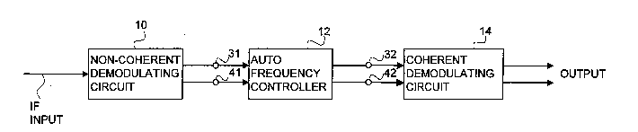
Fig. 2 is a block diagram of a demodulating device
according to an embodiment of the present invention.
In Fig. 2, a non-coherent demodulator 10 having
output terminals 31 and 41 includes the non-coherent
demodulator 1 and the local oscillator 2 which are shown
in Fig. 1, respectively. A coherent demodulator 14 is
composed of the coherent demodulator 5, the low-pass
filter (LPF) 6, the phase detector 7, the loop filter 8
and the VCO 9 which are those shown in Fig. 1, respectively.
Operations of these components 1, 2, 5- 9 are the same as
those described with reference to Fig. 1, respectively,
and the output terminals 31 and 41 of the non-coherent
demodulator 10 correspond to the output terminals 3 and 4
of the non-coherent demodulator 1 shown in Fig. 1.
Therefore, details thereof are omitted.
This embodiment of the present invention is featured
by an automatic frequency controller 12 provided between the
non-coherent demodulator 10 and the coherent demodulator 14.
The automatic frequency controller 12 serves to produce a
pseudo baseband signal whose frequency error is small, by
absorbing large frequency variation of receiving signal.
Fig. 3 shows the automatic frequency controller 12
shown in Fig. 2 in more detail.
In Fig. 3, a first pseudo baseband signal
exp~j(~(t)t+ ~(t))~ from the non-coherent demodulator 10,
which is a complex baseband signal containing frequency
error ~(t), is supplied through the terminals 31 and 41
- lO - 207693~
to a wide band PLL type demodulator 15. The wide band
PLL type demodulator 15 is composed of a first complex
multiplier including multipliers 16 and 17 and a ~/2
phase-shifter 21, a phase detector 18, a loop filter 19
and a first VCO 20.
The multiplier 16 multiplies the first pseudo
baseband signal from the terminal 31 with a signal
exp~-j~(t)t~ from the first VCO 20. The multiplier 17
multiplies the other first pseudo baseband signal from
the terminal 41 with the signal from the first VCO 20
phase-shifted by 90 by the ~/2 phase-shifter 21. The
phase detector 18 is of costas type and detects phase
error between the output signals of the multipliers 16
and 17. The loop noise bandwidth of the loop filter 19
is set as wide as fs/5 and the first voltage-controlled
oscillator 20 is controlled by the output signal - ~It)
of this loop filter 19.
Although this construction is responsible to a
receiving signal having large frequency variation, noise
may be increased since the loop noise bandwidth of the
loop filter 18 is very large. In order to solve this
noise problem, the output signal of the loop filter 19
is passed through a second LPF 26 to restrict noise
component thereof. A second VCO 27 is controlled by
the output -~'(t) of the LPF 26. A pass-band of the
low-pass filter 26 is preferably fs/200 aIthough other
pass band is also usable.
- 11- 2076935
The first pseudo baseband signals exp~(~(t)t + ~(t))~
from the terminals 31 and 41 supplied to the wide band PLL
type demodulator 15 are also supplied to a second complex
multiplier composed of multipliers 24 and 25 and a ~/2
phase shifter 28. The multiplier 24 multiplies the first
pseudo baseband signal from the terminal 31 with the
signal exp~-j~'(t)t~ from the second VCO 27 and a
resultant second pseudo baseband signal is supplied to
a terminal 32. The multiplier 25 multiplies the first
pseudo baseband signal from the terminal 41 with the
signal from the second voltage-controlled oscillator 27
which is phase-shifted by 90 by the ~/2 phase-shifter 28
and a resultant second pseudo baseband signal is provided
at a terminal 42.
- 15 The second pseudo baseband signals become
exp~ ~ (t)t + ~(t))~
where ~ ~(t) = ~'(t) - ~(t).
Since it is possible to make ~ ~ (t) very small,
complex baseband signals whose frequency error is minimized
are obtained.
In order to remove the effect of delay in the low-
pass filter 26, it may be possible to provide delay
circuits (D) 22 and 23 between the terminals 31 and 41
and the multipliers 24 and 25, respectively.
In Fig. 2, the second pseudo baseband signals from
the terminals 32 and 42 having smaller frequency errors
are supplied to the coherent demodulator 14 which is a
~ - 12 - 2076935
narrow band demodulator.
As described hereinbefore, in the present invention,
a first control signal for controlling the first VCO is
produced by the wide band PLL type demodulator and the
second VCO is controlled by a second control signal
obtained by removing noise component of the first control
signal. Then, the complex baseband signal whose frequency
error is small is produced by multiplying the complex
baseband signal containing frequency error with the output
signal of the second VCO and the complex baseband signal
having small frequency error is supplied to the narrow
band demodulator.
Therefore, it is possible to assure a proper
demodulating operation with respect to a receiving signal
whose carrier frequency variation is considerable.
- Although the present invention has been described
with reference to the specific embodiments, this description
is not meant to be construed in a limiting sense. Various
modifications of the disclosed embodiments, as well as
other embodiments of the present invention, will become
apparent to persons skilled in the art upon reference
to the description of the present invention. It is,
therefore, contemplated that the appended claims will
cover any modifications or embodiments as fall within
the true scope of the present invention.