Note : Les descriptions sont présentées dans la langue officielle dans laquelle elles ont été soumises.
2077155
APPARATUS FOR CONTROLLING CONSUMPTION POWER FOR GaAs FET
BACKGROUND OF THE INVENTION
The present invention relates to an apparatus for
controlling an electric power consumed by an amplifier
including a GaAs field effect transistor (FET), and in
particular to an apparatus for controlling an electric power
consumed by an amplifier including a GaAs FET capable of
minimizing a variation in gain, a variation in phase, and a
deviation of gain within a band for the amplifier.
Description of the Related Art
In a conventional apparatus for controlling an
electric power consumed by an amplifier including a GaAs FET,
a positive voltage having a fixed value is continuously
supplied from a power supply circuit to a drain region of the
GaAs FET and a negative voltage having a variable value is
delivered from a power supply to a gate region of the GaAs
FET. The negative voltage fed to the gate region is
controlled according to a value not less than a pinch-off
voltage of the GaAs FET to alter a source-to-drain or drain
current (ID), thereby controlling the power consumed by the
GaAs FET.
However, in the conventional power controller of
tllis type, the drain current is changed by varying the gate
voltage of the GaAs FET to control the power consumption,
which leads to considerably large changes respectively in the
gain, the phase, and the deviation of gain within a band.
The changes in the gain and phase cause an alteration in the
quantity of improvement of distortion; moreover, the
variation in the deviation minimizes a compensation
2077155
bandwidth of the GaAs FET. This consequently leads to a
drawback that in a linear amplifier in which a component of
intermodulation distortion appearing in an amplifier
including a multi-stage connection is compensated for by
cancelling the distortion component with a component having
an identical amplitude and an opposite phase with respect to
those of the distortion component, the compensation cannot
be easily achieved.
In order to improve the disadvantageous feature.
there is required quite a fine and complex control in
consideration of the gain and phase. which leads to a problem
that the hardware configuration and software system are
complicated and increased.
SUMMARY OF THE INVENTION
It is therefore an object of the present invention
to provide an apparatus for controlling an electric power
consumed by an amplifier including a GaAs FET capable of
effectively minimizing a variation in gain, a variation in
phase. and a deviation of gain within a band developed when
the consumed power is controlled. thereby solving the problem
above.
In accordance with the present invention. there is
provided a consumption power controlling apparatus for an
amplifier using a GaAs FET comprising first power source
means for supplying a positive direct-current voltage to a
drain region of the FET. second power source means for
supplying a negative direct-current voltage to a gate region
of the FET, variable voltage means connected to an output
terminal of the second power source means for variablY
2077155
- 3 -
controlling an output voltage from the second power source
means, resistor means having a terminal connected to an
output terminal of the first source means and another
terminal connected to the drain region of the FET. variable
resistor means having an adjusting member, the variable
resistor means having a terminal connected to the output
terminal of the first source means and another terminal
connected to an output terminal of the variable voltage
means the drain region of the FET, the adjusting member
being connected to the gate region of the FET; and control
means for detecting a voltage developed across the resistor
means for supplying a control voltage to the variable voltage
means, thereby setting the voltage to be substantiallY equal
to a preset reference value. The variable voltage means
controls, in response to the control signal from the control
means, the voltage supplied from the second power source
means to the gate of the FET, thereby keeping a drain current
of the FET at a constant value.
BRIEF DESCRIPTION OF THE DRAWINGS
The obiects and features of the present invention
will become more apparent from the consideration of the
following detailed description taken in coniunction with the
accompanying drawings in which:
Fig. 1 is a schematic block diagram showing the
configuration of an example of the consumption power
controlling apparatus of the prior art;
Fig. 2 is a graph showing changes respectively in
the gain, the phase, and the deviation of gain within a band
developed when the consumption power is controlled;
2077155
- 4 -
Fig. 3 is a block diagram schematically showing the
constitution of an embodiment of an apparatus for
controlling an electric power consumed by an amplifier
including a GaAs FET in accordance with the present
invention; and
Fig. 4 is a graph showing changes respectively in
the gain, the phase, and the deviation of gain within a band
developed when the consumption power is controlled in the
consumption power controlling apparatus of Fig. 3.
DESCRIPTION OF THE PREFERRED EMBODIMENTS
For better understanding of the present invention,
description will now be given of an apparatus for controlling
an electric power consumed by a conventional amplifier using
a GaAs FET.
Fig. 1 shows an apparatus for controlling an
electric power consumed by a conventional GaAs FET amplifier,
whereas Fig. 2 shows changes respectively in the gain, the
phase, and the deviation of gain within a band developed
when the consumption power is controlled in the power
consumption controlling apparatus of Fig. 1.
Conventionally, an apparatus for controlling an
electric power consumed by a GaAs FET amplifier includes, as
shown in Fig. 1, a power source circuit 1 for continuouslY
supplying a positive voltage having a fixed value to a drain
region of the GaAs FET 7, a power source circuit 2 for
supplying a negative voltage, and a variable voltage circuit
4 for controlling the negative voltage produced from the
power source circuit 2 to supply the controlled negative
voltage to a gate region of the GaAs FET. The negative
2077155
- 5 -
voltage fed from the variable voltage circuit 4 is controlled
according to a value not less than a pinch-off voltage of the
GaAs FET 7 to alter a drain current (ID), thereby controlling
the electric power consumed by the GaAs FET.
However, in such a conventional Power controlling
apparatus, the gate voltage of the GaAs FET is controlled by
a control signal supplied from an input terminal 8 to vary
the drain current, thereby supervising the consumed power.
Consequently, due to the Power control, there appear
considerably large changes respectively in the gain, the phase,
and the deviation of gain within a band as shown in Fig. 2.
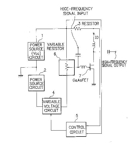
Fig. 3 shows the structure of the consumption power
controlling apparatus in an embodiment according to the
present invention.
The apparatus of Fig. 3 includes a first power
source circuit 1 for producing a positive direct-current
voltage, a second power source circuit 2 for producing a
negative direct-current voltage, a variable voltage circuit 4
having an input connected to an output from the power source
circuit 2 for controlling an output voltage from the power
source circuit 2 based on a control signal received from a
control circuit 5, and a GaAs FET 7 having a source region
connected to a common or shared potential.
Between an output terminal of the power source
circuit l and a drain region of the GaAs FET 7, there is
arranged a resistor 3. Between an output terminal of the
power source circuit l and an output terminal of the
variable voltage circuit 4, there is disposed a variable
resistor 6 having an adiusting member. The adjusting member
is connected to a gate region of the GaAs FET 7. The
- 6 - 2077155
resistor 3 is connected between two input terminals of the
control circuit 5. The control circuit 5 detects a voltage
developed across the resistor 3 and then compares the
voltage with a predetermined reference voltage. Depending
on a result of comparison, to set the detected voltage to be
substantially equal to the predetermined reference value,
the control circuit 5 delivers a control signal to the
variable voltage circuit 4.
Description will now be given of the operation of
lOthe consumption power controlling apparatus thus
constructed. Fig. 4 shows changes respectively in the gain,
the phase, and the deviation of gain within a band developed
when the consumption power is controlled in the consumption
power controlling apparatus according to the present invention.
15In the amplifier including a GaAs FET to be operated
with a source region thereof connected to a grounding
potential as shown in Fig. 3, the drain current (ID) is
generally controlled as follows. First, the variable voltage
circuit 4 is set to the minimum voltage and is then powered
from the power source circuit 2 so as to develop the negative
voltage representing a lowest value.
Next, the adjustable member of the variable resistor
6 is moved toward the side of the variable voltage circuit 4
to supply the lowest voltage to the gate region of the GaAs
FET 7; thereafter, the power source circuit l is turned on
to supply a positive voltage thereto. Thereafter, the
variable resistor 6 is adjusted so as to cause a
predetermined drain current (ID) to flow. For a regular
drain current (ID), there appears across the resistor 3 a
voltage drop which is a product (R ID) between the
2o77l5s
- 7 -
resistance R of the resistor 3 and the drain current ID.
Consequently. the control circuit 5 monitors the voltage drop
through the resistor 3 to control the variable voltage
circuit 4 so that the value of product (R ID) is
continuously kept retained at the predetermined reference
value. That is, the control circuit 5 includes a comparator
for comparing the value of voltage with the predetermined
reference value. Depending on a result of comparison. the
control circuit 5 sends a control signal to the variable
voltage circuit 4. thereby controlling the quantity of
voltage change in voltage to be developed by the variable
voltage circuit 4.
Next, a detailed description will be given
particularly of reduction of the power consumption in the
consumption power control according to the present invention.
As above. the apparatus is initiated to supPly the
gate region of the GaAs FET with the lowest voltage to
prevent a large drain current from flowing therethrough.
Thereafter. the adiusting member of the variable resistor 6
is moved to lower the voltage (Vcc) to be supplied from the
power source circuit l. When the voltage is decreased. the
gate voltage of the FET is also lowered and hence the drain
current (ID) is minimized. This means that the voltage
monitored by the control circuit 5 is reduced. The control
circuit 5 compares the predetermined reference voltage with
the product between the resistance R of the resistor 3 and
the drain current ID to continuously achieve the control
operation until there is attained a matching condition as a
result of comparison. thereby completing a cycle of control
operation. Until the preset consumption power is developed.
2077155
- 8 -
the control circuit 5 conducts several cycles of control
operation above.
In accordance with the present invention, there are
disposed resistor means arranged between an output terminal
of first power source means and a drain region of a GaAs FET
and variable resistor means having an adiusting member and
being arranged between output terminals respectively of the
first power source means and variable voltage means, the
adjusting member being connected to a gate region of the GaAs
FET. Control means having two input terminals between which
the resistor means is arranged supplies a control signal to
the variable voltage means, thereby controlling a voltage
developed across the resistor means to be substantially
equal to a predetermined reference value.
In consequence, since the drain current flowing
through the GaAs FET is set to be a fixed value, even when
the consumption power is controlled, the changes respectively
in the gain, the phase, and the deviation of gain within a
band can be satisfactorily minimized.
In the embodiment, for simplification of drawing, a
circuit for deleting a direct-current component from a high-
frequency signal supplied to the amplifier is shown in quite
a simplified form.
As above, in accordance with the present invention,
there can be attained an advantageous effect that the
changes respectively in the gain, the phase, and the
deviation of gain within a band can be satisfactorilY
minimized even when the consumption power is controlled.
Consequently, in a case where an amplifier to which the
consumption power controlling apparatus is applied to
2077155
g
compensate for the distortion. there need not be accomplished
the fine and complex control operation, thereb~ contributing
to minimization of the circuit.
While the present invention has been described with
reference to the particular illustrative embodiments, it is
not to be restricted by those embodiments but only by the
appended claims. It is to be appreciated that those skilled
in the art can change or modify the embodiments without
departing from the scope and spirit of the present invention.