Note : Les descriptions sont présentées dans la langue officielle dans laquelle elles ont été soumises.
2078038
MEASUREMENT OF RECEIVER SENSITIVITY
OF A RADIO COMMUNICATION APPARATUS
BY RADIO AND OPTICAL TEST SIGNALS
Background of the Invention:
This invention relates to a radio communication
apparatus for use in combination with a test transmitter
for testing the radio communication apparatus in order to
measure a receiver sensitivity of the radio communication
apparatus. This invention relates also to the test
transmitter. The radio communication apparatus may be a
radio paging receiver, a transceiver, or the like
although description will be mainly directed to the radio
paging receiver.
A radio paging receiver of the type described, is
for receiving a radio communication signal which carries
a communication digital data signal. The radio paging
receiver generally comprises a radio digital data
recovering section for recovering the communication
digital data signal from the radio communication signal.
Connected to the radio digital data recovering section, a
data processing section processes the communication
digital data signal into a processed~data signal.
Connected to the data processing section, an announcing
section carries out an announcing operation of producing
2 2078038
an announcement to an attendant to the radio paging
receiver in response to the processed data signal.
A test transmitter of the type described,
generally comprises a test signal generator for
generating a test digital data signal. Connected to the
test signal generator, a radio test signal transmitting
section transmits the radio test signal which carries the
test digital data signal.
On using the test transmitter in testing the
radio paging receiver so as to measure a receiver
sensitivity of the radio paging receiver in relation to
the communication digital data signal, the test digital
data signal is made to represent an identlfication number
specific to the radio paging receiver.
When the radio test signal has a high electric
field strength, the radio paging receiver can correctly
receive the test digital data signal with the test
digital data signal subjected to no'bit error. In this
case, the radio digital data recovering section correctly
recovers the test digital data signal from the radio test
signal in the radio paging receiver. The data processing
section processes the test digital data signal into the
processed data signal. The announcing section duly
carries out the announcing operation.
When the radio test signal has a low electric
field strength, the radio paging receiver may receive the
test digital data signal with the test digital data
signal subjected to bit errors. Inasmuch as the radio
~, . .~,,
3 2078038
paging receiver can not correctl~y rece-ive the test
digital data signal in this case, the data processing
section does not produce the processed data signal. The
announcing section does not carry out the announcing
operation.
Conventionally, the receiver sensitivity of the
radio paging receiver is defined as a lowest electric
field strength in which the radio paging receiver can
carry out the announcing operation. Inasmuch as the
receiver sensitivity (that is, the lowest electric field
strength of the radio test signal) is determined by
judging whether or not the radio paging receiver carries
out the announcing operation, it is necessary to make the
test signal generator of the test transmitter generate
the test digital data signal which represents the
identification number specific to the radio paging
receiver. When a different radio paging receiver is
tested, it is necessary to make the test signal generator
generate the test digital data signal which represents a
different identification number specific to the different
radio paging receiver. This results in an increase in
labor and time of measurement of the receiver sensitivity
in proportion to an increase in the number of the radio
paging receivers.
Furthermore, it is difficult to quantitatively
know the number of either correct bits or erroneous bits
in the test digital data signal carried by the radio test
signal which the radio paging receiver receives when the
4 2078038
radio test signal has a particular electric field
strength between the high electric field strength and the
low electric field strength.
Summary of the Invention:
It is therefore an object of this invention to
provide a radio communication apparatus operable in
combination with a test transmitter, which apparatus is
capable of quantitatively measuring, as a receiver
sensitivity of the radio communication apparatus, the
number of correct or nonerroneous bits in a test digital
data signal carried by a radio test signal which the
radio communication apparatus Ee~eives when the radio
- test signal has a particular electric field strength.
It is another object of this invention to provide
a radio communication apparatus of the type described,
wherein it is unnecessary to make a test signal generator
of the test transmitter generate the test digital data
signal which represents an identification number specific
to the radio communication apparatus.
It is still another object of this invention to
provide a radio communication apparatus of the type
described, wherein it is possible to decrease labor and
time of measurement of the receiver sensitivity of the
radio communication apparatus.
It is a further object of this invention to
provide a test transmitter for use in combination with a
radio communication apparatus, which test transmitter is
capable of quantitatively measuring, as a receiver
207803-8
sensitivity of the radio communication apparatus, the
number of correct bits in a test digital data signal
carried by a radio test signal which the radio
communication apparatus receives when the radio test
signal has a particular electric field strength.
It is a still further object of this invention to
provide a test transmitter of the type described, wherein
it is unnecessary to make a test signal generator of the
~est transmitter generate the test digital data signal
which represents an identification number specific to the
radio communication apparatus.
It is a yet further object of this invention to
provide a test transmitter of the type described, wherein
it is possible to decrease labor and time of measurement
of the receiver sensitivity of the radio communication
apparatus.
Other objects of this invention will become e~e~r
as the description proceeds.
On describing the gist of an aspect of this
invention, it is possible to understand that a radio
communication apparatus is for receiving a radio
communication signal carrying a communication digital
data signal and a radio test signal carrying a test
digital data signal. The radio communication apparatus
includes radio digital data recovering means for
recovering the communication digital data signal from the
radio communication signal and the test digital data
signal as a first digital data signal from the radio test
'. ,~
2078~3-8
signal.
According to this aspect of this invention, the
above-understood radio communication apparatus is for
receiving an optical test signal carrying the test
digital data signal. The radio communication apparatus
comprises optical digital data recovering means for
recovering the test digital data signal as a second
digital data signal from the optical test signal, timing
pulse generating means connected to the optical digital
data recovering means for generating a timing pulse
signal in bit synchronism with the second digital data
signal, comparing means connected to the radio and the
optical digital data recovering means for comparing the
first digital data signal with the second digital data
signal bit by bit to successively produce bit coincidence
pulses whenever the first and the second digital data
signals are coincident with each other bit by bit, a
first counter connected to the timing pulse generating
means for counting up a first count in response to the
timing pulse signal from an initial value to a
predetermined threshold value to produce a count stop
signal when the first count is counted up to the
threshold value, and a second counter connected to the
comparing means and the first counter for counting up a
second count in response to the bit coincidence pulses
from an initial count to an increased count until
production of the count stop signal to produce a count
signal which represents the increased count as a receiver
~7 2078038
sensitivity of the radio communication apparatus in
relation to the communication digital data signal.
On describing the gist of a specific aspect of
this invention, it is possible to understand that a radio
communication apparatus is for receiving a radio
communication signal carrying a communication digital
data signal. -The radio communication apparatus is for
use in combination with a test transmitter including a
test signal generator for generating a test digital data
signal, and radio test signal transmitting means
connected to the test signal generator for transmitting a
radio test signal carrying the test digital data signal.
The radio communication apparatus includes radio digital
data recovering means for recovering the communication
digital data signal from the radio communication signal
and the test digital data signal as a receiver recovered
digital data signal from the radio test signal.
According to the specific aspect of this
invention, the above-understood radio communication
apparatus comprises optical test signal transmitting
means connected to the radio digital data recovering
means for transmitting an optical test signal carrying
the receiver recovered digital data signal. The test
transmitter comprises optical digital data recovering
means for recovering the receiver recovered digital data
signal as a transmitter recovered digital data signal
from the optical test signal, timing pulse generating
means connected to the test signal generator for
A
8 2078038
generating a timing pulse signal in bit synchronism with
the test digital data signal, comparing means connected
to the test signal generator and the optical data
recovering means for comparing the transmitter recovered
digital data signal with the test digital data signal to
successively produce bit coincidence pulses whenever the
test digital data signal and the transmitter recovered
digital data signal are coincident with each other bit by
bit, a first counter connected to the timing pulse
generating means for counting up a first count in
response to the timing pulse signal from an initial value
to a predetermined threshold value to produce a count
stop signal when the first count is counted up to the
threshold value, and a second counter connected to the
comparing means and the first counter for counting up a
second count in response to the bit coincidence pulses
from an initial count to an increased count until
production of the count stop signal to produce a count
signal which represents the increased count as a receiver
sensitivity of the radio communication apparatus in
relation to the communication digital data signal.
On describing the gist of a different aspect of
this invention, it is possible to understand that a test
transmitter for use in testing radio communication
apparatus for receiving a radio communication signal
carrying a communication digital data signal. The test
transmitter includes a test signal generator for
generating a test digital data signal, and radio test
9 2078d3-8
signal transmitting means connected to the test signal
generator for transmitting a radio test signal carrying
the test digital data signal. The radio communication
apparatus includes radio digital data recovering means
for recovering the communication digital data signal from
the radio communication signal and the test digital data
signal as a receiver recovered digital data signal from
the radio test signal.
According to the different aspect of this
invention, the above-understood test transmitter
comprises optical digital data recovering means for
recovering the receiver recovered digital data signal as
a transmitter recovered digital data signal from an
optical test signal carrying the receiver recovered
digital data signal, the optical test signal being
transmitted by optical test signal transmitting means
which is connected to the radio digital data recovering
means in the radio communication apparatus, timing pulse
generating means connected to the test signal generator
for generating a timing pulse signal in bit synchronism
with the test digital data signal, comparing means
connected to the test signal generator and the optical
data recovering means for comparing the transmitter
recovered digital data signal with the test digital data
signal to successively produce bit coincidence pulses
whenever the test digital data signal and the transmitter
received digital data signal are coincident with each
other bit by bit, a first counter connected to the timing
'~' ,A
20780~3-8
pulse generating means for counting up a first count in
response to the timing pulse signal from an initial value
to a predetermined threshold value to produce a count
stop signal when the first count is counted up to the
threshold value, and a second counter connected to the
comparing means and the first counter for counting up a
second count in response to the bit coincidence pulses
from an initial count to an increased count until
production of the count stop signal to produce a count
signal which represents the increased count as a receiver
sensitivity of the radio communication apparatus in
relation to the communication digital data signal.
Brief Description of the Drawing:
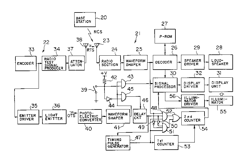
Fig. 1 is a block diagram of a combination of a
test transmitter, a base station, and a radio paging
receiver according to a first embodiment of this
invention;
Fig. 2 is a signal format for use in describing
, operation of the radio paging receiver illustrated in
Fig. l;
Fig. 3 is a time chart for use in describing
operation of the radio paging receiver illustrated in
Fig. l;
Fig. 4 is another time chart for use in
describing operation of the radio paging receiver
illustrated in Fig. l;
Fig. 5 is a block diagram of a radio paging
receiver according to a second embodiment of this
A
11 2078038
invention;
Fig. 6 is a block diagram of a radio paging
receiver according to a third embodiment of this
invention; and
Fig. 7 is a block diagram of a combination of a
radio paging receiver according to a fourth embodiment of
this invention and a test transmitter according to a
fifth embodiment of this invention.
Description of the Preferred Embodiments:
Referring to Fig. 1, a radio paging system
comprises a base station 20, a radio paging receiver 21
according to a first embodiment of this invention, and
other radio paging receivers (not shown) which are
similar in structure and in operation to the radio paging
receiver 21. The base station 20 is for transmitting a
radio communication signal indicated at RCS. The radio
paging receiver 21 receives and deals with the radio
communication signal RCS. The radio paging receiver 21
is for use in combination with a test transmitter 22
which will later be described.
Turning to Fig. 2, the radio communication signal
RCS is illustrated. The illustrated radio communication
signal RCS is a POGSAG code radio signal which is set up
in CCIR recommendation 584. The radio communication
signal RCS comprises a plurality of frames which are
similar in frame structure to one another.
Each frame of the radio communication signal RCS
carries a synchronization signal SYN and first through
12 2078038
q-th subframes SFl to SFq successively succeeding the
synchronization signal SYN, where q represents a positive
integer. The synchronization signal SYN has a
predetermined number of bits and is specified by a
predetermined pattern of bits.
The radio paging receiver 21 (Fig. 1) and other
radio paging receivers of the radio paging system have
identification or call numbers different from one another
and may be grouped into first through q-th groups. The
first through the q-th groups are assigned to the first
through the q-th subframes SFl to SFq of each frame,
respectively. Supposing that the radio paging receiver
21 belongs to the first group, the base station 20 tFig.
1) transmits a call number signal CN representative of
the identification or call number specific to the radio
paging receiver 21 and a communication message signal CME
representative of a communication message directed to the
radio paging receiver 21 by using the first subframe SFl.
The call number signal CN has first through P-th bits,
where P represents a natural number greater than one.
The communication message signal CME has a preselected
number of bits. Each of the synchronization signal SYN,
the call number signal CN, and the communication message
signal CME consists of Bose-Chaudhuri-Hocquenghem (BCH)
codes.
A combination of the synchronization signal SYN,
the call number signal CN, and the communication message
signal CME will be referred to herein as a communication
13 2078038
digital data signal. The communication digital data
signal is carried by the radio communication signal RCS.
Turning back to Fig. 1 with reference to Fig. 2
continued, description will be made as regards operation
of the radio paging receiver 21 when the paging receiver
21 receives the radio communication signal RCS. The
radio communication signal RCS is picked up by an antenna
23 and supplied to a radio section 24. The radio section
24 converts or demodulates the radio communication signal
RCS into a baseband or demodulated signal. Connected to
the radio section 24, a first waveform shaper 25 shapes
the demodulated signal into a shaped signal of a digital
waveform. The shaped signal has the communication
digital data signal (namely, a combination of the
synchronization signal SYN, the call number signal CN,
and the communication message signal CME).
Thus, a combination of the antenna 23, the radio
section 24, and the first waveform shaper 25 serves as a
radio digital data recovering section. The radio digital
data recovering section (23, 24, 25) is for recovering
the communication digital data signal from the radio
communication signal RCS.
A decoder 26 is supplied with the communication
digital data signal and detects the synchronization
signal SYN in order to establish bit synchronization and
frame synchronization. After the bit synchronization and
frame synchronization are established, the decoder 26
cooperates with a P-ROM (programmable read-only memory)
14 2078038
27 which preliminarily memorizes first through P-th bits
of a directory number signal representative of the
identification number specific to the radio paging
receiver 21. That is, the decoder 26 compares the call
number signal CN with the directory number signal bit by
bit.
When the decoder 26 detects coincidence between
the bits of the call number signal CN with the directory
number signal, the decoder 26 sends a speaker~drive
signal to a loudspeaker 28 through a speaker driver 29 to
make the loudspeaker 28 generate a call tone indicative
of a call to the radio paging receiver 21 a predetermined
time duration. Simultaneously, the decoder 26 sends the
communication message signal CME to a signal processor
30. Responsive to the communication message signal CME,
the signal processor 30 makes the display unit 31
visually display the communication message of the
communication message signal CME through a display driver
32. The display unit 31 is, for example, a liquid
crystal display (LCD).
Thus, the decoder 26 serves, in cooperation with
the P-ROM 27, the speaker driver 29, the signal processor
30, -and the display driver 32 as a data processing
section connected to the radio digital data recovering
section (23, 24, 25). The data processing section (26,
27, 29, 30, 32) processes the communication digital data
signal into a processed signal (namely, the speaker drive
signal and the communication message signal CME). A
A
207803-8
combination of the loudspeaker 28 and the display unit 31
serves as an announcing section connected to the data
processing section (26, 27, 29, 30, 32). The announcing
section (28, 29) carries out an announcing operation of
production of the processed data signal in response to
the processed data signal.
Turning to Fig. 3 with reference to Fig. l
continued, description will proceed to the test
transmitter 22. The test transmitter 22 is for use in
testing the radio paging receiver 21. The test
transmitter 22 is usually carried by a maintenance
engineer who is in charge of maintenance service of the
radio paging system. The test transmitter 22 is for
transmitting a radio test signal which is indicated at
RTS and which carries a test digital data signal. The
test transmitter 22 ~s furthermore for transmitting an
optical test signal indicated at OTS. The optical test
signal OTS carries the test digital data signal like the
radio test signal RTS.
The test transmitter 22 has an encoder 33 which
generates the test digital data signal having logic "l"
and "0" levels. More specifically, the test digital data
signal successively comprises first through N-th bits,
where N represents a first integer which is greater than
one.
The test digital data signal is illustrated in
Fig. 3 along a first or top line. The illustrated test
digital data signal successively comprises logic "0",
~.,.. ~
16 20 78038
"1", "1", "0", "0", "1", and "0" levels.
In Fig. 1, the encoder 33 simultaneously supplies
the test digital data signal to a radio test signal
producer 34 and to an emitter driver 35 for driving a
light emitter 36 which is, for example, an LED
(light-emitting diode), a laser diode, or the like.
When supplied with the test digital data signal,
the radio test signal producer 34 produces the radio test
signal RTS carrying the test digital data signal. The
radio test signal RTS is transmitted through an
attenuator 37 and an antenna 38.
When supplied with the test digital data signal,
the emitter driver 35 produces an on-off drive signal
which indicates on and off when the test digital data
signal has logic "1" and "0" levels, respectively.
Responsive to the on-off drive signal, the light emitter
36 emits or transmits a flicker light which indicates
logic "1" and "0" levels of the test digital data signal
as the optical test signal OTS carrying the test digital
data signal. More specifically, the optical test signal
OTS is controlled or modulated by the test digital data
signal to form the flicker light which indicates logic
"1" and "0" levels of the test digital data signal.
~With reference to Figs. 1 and 3 continued,
description will be made as regards operation of the
radio paging receiver 21 when the radio paging receiver
21 is tested by the test transmitter 22. In this event,
the maintenance engineer puts a switch 39 in an on state
-
17 2078038
and makes the test transmitter 22 transmit the radio and
the optical test signals RTS and OTS.
The radio test signal RTS is picked up by the
antenna 23 and supplied to the radio section 24. The
radio section 24 converts or demodulates the radio test
signal RTS into a baseband or demodulated signal. The
demodulated signal is illustrated in Fig. 3 along a
second line. The illustrated demodulated signal is
demodulated by the radio section 24 when the radio test
signal RTS has a high electric field strength.
In Fig. 1, the first waveform shaper 25 shapes
the demodulated signal into a first shaped signal of a
digital waveform by comparing the demodulated signal with
a predetermined threshold level illustrated in Fig. 3
along the second line. The first shaped signal will be
referred to as a first digital data signal and is
illustrated in Fig. 3 along a third line. The first
digital data signal has a high level when the demodulated
signal has an amplitude larger than the threshold level.
When the demodulated signal has another amplitude which
is not larger than the threshold level, the first digital
data signal has a low level. The illustrated first
digital data signal is equivalent in waveform to the test
digital data signal produced by the encoder 33. That is,
the radio paging receiver 21 correctly receives the test
digital data signal with the test digital data signal
subjected to no bit error. However, a time difference or
delay between the test digital data signal and the first
A
18 207803-8
digital data signal inevitably produces due to a circuit
delay of the radio section 24, the first waveform shaper
25, and so on.
As illustrated in Fig. 3 along a fourth line, the
demodulated signal is demodulated by the radio section 24
when the radio test signal RTS has a low electric field
strength. In this case, the first waveform shaper 25
produces the first digital data signal illustrated in
Fig. 3 along the fifth line. The illustrated first
digital data signal successively comprises logic "0",
"1", "1", "0", "1", "1", and "0" levels. That is, the
radio paging receiver 21 receives the test digital data
signal with the test digital data signal subjected to a
bit error. In the illustrated example, the bit error
occurs at a fifth bit of the first digital data signal.
Thus, the radio digital data,recovering section
(23, 24, 25) is furthermore for recovering the test
digital data,signal as the first digital data signal from
the radio test signal RTS.
A photoelectric converter 40 converts the optical
test signal OTS into a converted or demodulated signal.
Connected to the photoelectric converter 40, a second
waveform shaper 41 shapes the converted signal into a
second shaped signal of digital waveform that is
equivalent to the test digital data signal. Inasmuch as
the optical test signal OTS has no relation to the
electric field strength, the optical test signal OTS can
be received with the test digital data signal subjected
~' .
` -
19 ..~ 2078038
to no bit error. The second shaped signal has a waveorm
substantially equivalent to the shaped signal illustrated
in Fig. 3 along the third line.
In Fig. 1, the switch 39 has negative and
positive terminals connected to the earth or ground
directly and a voltage source through a resistor 42,
respectively. The voltage source is indicated at +V and
gives a positive voltage to the positive terminal. The
negative terminal is supplied with an earth voltage. It
will be assumed that the positive and the earth voltages
corresponding to a logic "1" level and a logic "0" level.
The switch 39 is usually put in an off state.
That is, the switch 39 is put in the off state when the
radio and the optical test signals RTS and OTS are not
transmitted by the test transmitter 22. In this case, a
first AND circuit 43 is supplied with-the logic "1" level
through the resistor 42. Inasmuch as an inverter 44 is
supplied with the logic "1" level through the resistor 42
and inverts the logic "1" level into the logic "0" level,
a second AND circuit 45 is supplied with the logic "0"
level. The first AND circuit 43 thereby delivers to the
signal processor 30 an output signal of the second
waveform shaper 41. In this event, the signal processor
30 operates in the manner which will later be described.
Turning to Fig. 4 with reference to Fig. 1
continued, description will proceed to a case where the
switch 39 is put in the on state. As mentioned above,
the switch 39 is put in the on state by the maintenance
,
`- 2078038
engineer when the radio paging receiver 21 is tested by
the test transmitter 22. In this case, the earth voltage
(namely, the logic "0" level) is supplied to the inverter
44 through the switch 39. Inasmuch as the inverter 44
supplies the second AND circuit 45 with the logic "1"
level, the second AND circuit 45 supplies a delay circuit
46 with the second shaped signal produced by the second
waveform shaper 41. The delay circuit 46 gives the
second shaped signal of the second waveform shaper 41 a
predetermined delay so that the first bit of the shaped
signal of the second waveform shaper 41 coincides with
the first bit of the first digital data signal produced
by the first waveform shaper 25. The delay circuit 46
thereby produces a delayed signal which will be referred
to as a second digital data signal.
Thus, a combination of the photoelectric
converter 40, the second waveform shaper 41, the switch
39, the voltage source +V, the resistor 42, the inverter
44, the second AND circuit 45, and the delay circuit 46
is operable as an optical digital data recovering
section. The optical digital data recovering section
(39-42, +V, 44-46) recovers the test digital data signal
as the second digital data signal from the optical test
signal OTS.
In Fig. 4, the test digital data signal produced
by the encoder 33 is illustrated along a first line.
First through seventh bits of the illustrated test
digital data signal have the logic "0", "1", "1", "0",
21 j 2078038
"0", "1", and "0" levels, respectively.
As illustrated in Fig. 4 along a second line, the
second digital data signal produced by the delay circuit
46 of the optical digital data recovering section has a
waveform which is substantially equivalent to the test
digital data signal. This is because the optical test
signal OTS can be received with the test digital data
signal subjected to no bit error as mentioned above.
The first digital data signal produced by the
first waveform shaper 25 of the radio digital data
recovering section (23, 24, 25) is illustrated in Fig. 4
along a third line. The illustrated first digital data
signal is equivalent to the first digital data signal
illustrated in Fig. 3 along the fifth line and has the
bit error which occurs at the fifth bit of the first
digital data signal as mentioned above.
In Fig. 1, a timing pulse generator 47 is
connected to the delay circuit 46 of the optical digital
data recovering section (39-42, +V, 44-46). The timing
pulse generator 47 generates a timing pulse signal in bit
synchronism with the second digital data signal. More
specifically, the timing pulse generator 47 successively
generates first through N-th timing pulses collectively
as the timing pulse signal in bit synchronism with the
2S first through the N-th bits of the second digital data
signal. The timing pulse signal is illustrated in Fig. 4
along a fifth line.
2078038
In Figs. 1 and 4, a third AND circuit 48 is
directly connected to the first waveform shaper 25, the
delay circuit 46, and the timing pulse generator 47. The
third AND circuit 48 successively produces first
coincidence pulses whenever n-th bits of the first and
the second digital data signals and an n-th timing pulse
are coincident with one another, where n consecutively
varies from 1 to N. In this event, each of the first
coincidence pulses is produced when the n-th bit of the
first digital data signal and the n-th bit of the second
digital data signal have the logic "1" level in common.
Connected to the first waveform shaper 25 and the
delay circuit 46 through inverters 49 and 50,
respectively, and connected to the timing pulse generator
47 directly, a fourth AND circuit 51 successively
produces second coincidence pulses whenever inverted bits
of the n-th bits of the first and the second digital data
signals and the n-th timing pulse are coincident with one
another. In this event, each of the second coincidence
pulses is produced when the n-th bit of the first digital
data signal and the n-th bit of the second digital data
signal have the logic "0" level in common.
Connected to the third and the fourth AND
circuits 48 and 51, an OR circuit 52 produces the first
and the second coincidence pulses as bit coincidence
pulses. In Fig. 4, the bit coincidence pulses are
illustrated along a fifth line.
23 2078038
Thus, a combination of the third and the fourth
AND circuits 48 and 51, the inverters 49 and 50, and the
OR circuit 52 serves as a comparing section connected to
the radio digital data recovering section (23, 24, 25)
and the optical digital data recovering section (39-42,
44, 45, +V). The comparing section (48-52) compares the
first digital data signal with the second digital data
signal bit by bit and successively produces the bit
coincidence pulses whenever the first and the second
digital data signals are coincident with each other bit
by bit. More specifically, the comparing section (48-52)
compares the first through the N-th bits of the first
digital data signal with the first through the N-th bits
of the second digital data signal, respectively, and
successively produces the bit coincidence pulses whenever
n-th bits of the first and the second digital data
signals are coincident with each other, where n
consecutively varies from 1 to N.
In Fig. 1, a first counter 53 is connected to the
timing pulse generator 47. The first counter 53 counts
up a first count in response to the timing pulse signal
from an initial value to a predetermined threshold value
and produces a count stop signal when the first count is
counted up to the threshold value. The threshold value
is greater than the in-itial value by a second integer M
which is greater than one and is not greater than the
first integer N. More specifically, the first counter 53
counts up the first count to at least a part of the first
A
24 2078038
through the N-th timing pulses and produces the count
stop signal when the first count increases up to the
threshold value.
Connected to the OR circuit 52 of the comparing
section (48-52) and the first counter 53, a second
counter 54 counts up a second count in response to the
bit coincidence pulses from an initial count equal to
zero to an increased count until production of the count
stop signal and produces a count signal which represents
the increased count as a receiver sensitivity of the
radio paging receiver 21 in relation to the communication
digital data signal. More specifically, the second
counter 54 counts up the second count in response to the
bit coincidence pulses which are produced when n
consecutively varies from 1 towards N. The second
counter 54 produces the count signal.
Connected to the second counter 54, the signal
processor 30 makes the display unit 31 display, as the
receiver sensitivity of the radio paging receiver 21, the
increased count of the count signal through the display
driver 32. Supposing that the second integer M is equal
to 100, the display unit 31 displays the number of bit
coincidence pulses produced during a time duration
corresponding to 100 timing pulses. In this case, the
display unit 31 displays percentage of the number of
correct or nonerroneous bits in the test digital data
signal carried by the radio test signal RTS which the
radio paging receiver 21 receives when the radio test
.~ ' .
2 0 7 8 0 3 8
signal RTS has a particular electric field strength.
Thus, a combination of the signal processor, the
display driver 32, and the display unit 31 is operable as
an indicating section connected to the second counter 54.
The indicating section (30, 31, 32) indicates, as the
receiver sensitivity of the radio paging receiver 21, the
increased count represented by the count signal.
In Fig. 1, the radio paging receiver 21 further
comprises an illuminator 55, such as a lamp, connected to
the signal processor 30 through an illuminator driver 56.
The illuminator 55 illuminates the display unit 31 by
illuminating light when the illuminator 55 is driven by
the signal processor 30. As mentioned above, the signal
processor 30 is supplied with the output signal of the
second waveform shaper 41 through the AND circuit 43 when
the switch 39 is put in the off state. Inasmuch as the
maintenance engineer does not make the test transmitter
22 transmit the optical test signal OTS when the switch
39 is put in the off state, the photoelectric converter
40 is not supplied with the optical test signal OTS but
supplied with environment light of the paging receiver
21. When the environment light has a low intensity or
brightness, the output signal of the second waveform
shaper 41 has a logic "1" level. When the environment
light has a high intensity or brightness, the output
signal of the second waveform shaper 41 has a logic "0"
lcvcl. That is, when environment of the radio paging
receiver 21 becomes dark, the output signal of the second
`'" .A .
26 2078038
waveform shaper 41 has a logic "1" level. On condition
that the signal processor 30 receives the output signal
of the logic "1" level from the second waveform shaper 41
through the first AND circuit 43 (namely, the environment
of the radio paging receiver 21 becomes dark) when the
signal processor 30 drives the display unit 31 so as to
make the display unit 31 display the communication
message CME (Fig. 2) recovered by the decoder 26, the
signal processor 30 drives the illuminator 55 to make the
illuminator 55 illuminate the display unit 31 by the
illuminating light.
Turning to Fig. 5, description will proceed to a
radio paging receiver 60 according to a second embodiment
of this invention. The radio paging receiver 60
comprises similar parts designated by like reference
numerals. The radio paging receiver comprises a mode
selector 61 which selects a normal and a test mode of
operation. The normal and the test mode are indicated at
N and T, respectively. First through third selectors 62,
63, and 64 are connected to the mode selector 61. Each
of the first through the third selectors 62 to 64 selects
a normal mode N of operation when the mode selector 61
selects the normal mode N. When the mode selector 61
selects the test mode T, each of the first through the
third selectors 62 to 64 selects a test mode T of
operation.
A combination of the mode selector 61 and the
first through the third selectors 62 to 64 will be
27 20780~-8
referred to as a mode selecting section for selecting the
normal and the test mode of operation.
It will be assumed that the maintenance engineer
makes the mode selector 61 select the test mode T and
that the test transmitter 22 transmits the radio and the
optical test signals RTS and OTS. In this case, the
first through the third selectors 62 to 64 selects the
test mode T.
In the test mode T, the timing pulse generator 47
is connected to the second waveform shaper 41 of the
optical digital data recovering section (40, 41) through
the first selector 62 of the mode selecting section
(61-64). As a result, the timing pulse generator 47
successively generates the first through the N-th timing
pulses in bit synchronism with the first through the N-th
bits of the second digital data signal recovered by the
second waveform shaper 41 of the optical digital data
recovering section (40, 41).
A comparing section 65 is connected to the first
waveform shaper 25 of the radio digital data recovering
section (23-25) directly and to the timing pulse
generator 47 directly. The comparing section 65 is
furthermore connected to the second waveform shaper 41 of
the optical digital data recovering section (40, 41)
through the second selector 63 of the mode selecting
section (61-64) in the test mode T.. Like the comparing
section (48-52) of the radio paging receiver 21 of Fig.
1, the comparing section 65 compares, in the test mode T,
A
28 2078038
the first through the N-th bits of the first digital data
signal from the first waveform shaper 25 with the first
through the N-th bits of the second digital data signal
from the second waveform shaper 41, respectively, and
successively produces the bit coincidence pulses whenever
the n-th bits of the first and the second digital data
signals are coincident with each other, where n
consecutively varies from 1 to N.
The second counter 54 is connected to the
comparing section 65 through the third selector 64 of the
mode selecting section (61-64) in the test mode T. Like
in the radio paging receiver 21, the second counter 54
counts up the second count until production of the count
stop signal from the first counter 53 in response to the
bit coincidence pulses which are produced when n
consecutively varies from 1 to N. The second counter 54
produces the count signal which represents the increased
count as a receiver sensitivity of the radio paging
receiver 60.
Connected to the mode selector 61 and responsive
to the count signal, the signal processor 30 makes the
display unit 31 display the increased count of the count
signal as the receiver sensitivity of the radio paging
receiver 60 in the test mode T.
It will be assumed that the mode selector 61
selects the normal mode N and that the radio paging
receiver 60 receives the radio communication signal RCS
instead of the radio and the optical test signals RTS and
~,t_ ,~, 4
i~_ 29 20780~`8
OTS. In this case, the first through the third selectors
62 to 64 selects the normal mode N.
As mentioned above, the communication digital
data signal is carried by the radio communication signal
RCS and comprises the call number signal CN (Fig. 2)
having the first through the P-th bits.
The P-ROM 27 produces a specific digital data
signal successively comprising first through P-th bits in
synchronism with the first through the P-th bits of the
communication digital data signal. The first through the
P-th bits of the specific digital data signal
collectively represents the identification number
specific to the radio paging receiver 60.
In the normal mode N, the timing pulse generator
47 is connected to the first waveform shaper 25 of the
radio digital data recovering section (23-25) through the
first selector 62 of the mode selecting section (61-64)
and to the P-ROM 27 through a signal supply lead 66. As
a result, the timing pulse generator 47 successively
generates first through P-th timing pulses in bit
synchronism with the first through the P-th bits of the
communication digital data signal recovered by the first
waveform shaper 25 of the radio digital data recovering
section (23-25).
The comparing section 65 is connected to the
P-ROM 27 through the second selector 63 of the mode
selecting section (61-64) and is connected to the first
waveform shaper 25 of the radio digital data recovering
2078038
section (23-25) directly and to the timing pulse
generator 47 directly. In the manner similar to
operation of the comparing section 65 in the test mode T,
the comparing section 65 compares, in the normal mode N,
the first through the P-th bits of the communication
digital data signal from the first waveform shaper 25
with the first through the P-th bits of the specific
digital data signal from the P-ROM 27, respectively, and
successively produces output coincidence pulses whenever
p-th bits of the communication and the specific digital
data signals are coincident with each other, where p
consecutively varies from 1 to P.
More specifically, the P-ROM 27 memorizes first
through P-th bits of a directory number signal
representative of the identification number specific to
the radio paging receiver 60 like in the radio paging
receiver 21 of Fig. 1. The signal supply lead 66 is
connected to the timing pulse generator 47 and to the
P-ROM 27 for supplying the first through the P-th timing
pulses to the P-ROM 27 to make the P-ROM 27 produce the
first through the P-th bits of the directory number
signal in bit synchronism with the first through the P-th
timing pulses as the first through the P-th bits of the
specific digital data signal.
In the normal mode N, a specific counter 67 is
connected to the comparing section 65 through the third
selector 64 of the mode selecting section (61-64) and to
~- the timing pulse generator 47 directly. With reference
~,~.. ~
.
31 2078038
to the first through the P-th timing pulses in bit
synchronism with the first through the P-th bits of the
communication digital data signal, the specific counter
67 counts the output coincidence pulses produced in
response to the first through the P-th bits of the
specific digital data signal. The specific counter 67
thereby produces a number coincidence signal which
indicates that the first through the P-th bits of the
communication digital data signal represents the
identification number specific to the radio paging
receiver 60.
The specific counter 67 supplies the number
coincidence signal to the loudspeaker 28 through the
speaker driver 29 as the speaker drive signal to make the
loudspeaker 28 generate the call tone indicative of a
call to the radio paging receiver 60 a predetermined time
duration.
. The specific counter 67 supplies the number
coincidence signal to a switching circuit 68 labelled
"SW". In response to the number coincidence signal, the
switching circuit 68 sends to the signal processor 30 the
communication message signal CME (Fig. 2) which follows
the call number signal CN. Responsive to the
communication message signal CMR, the signal processor 30
makes the display unit 31 display the communication
message of the communication message signal CME through
the display driver 32.
32 2078038
Turning to Fig. 6, description will proceed to a
radio paging receiver 70 according to a third embodiment
of this invention. The radio paging receiver 70
comprises similar parts designated by like reference
numerals.
Like in the radio paging receiver of Fig. 1, the
switch 39 is usually put in the off state and is put in
the on state when the radio paging receiver 70 is tested.
The switch 39 corresponds to the mode selector 61 of Fig.
5 and operates in the manner similar to the mode selector
61.
In the radio paging receiver 70, the first
through the third selectors 62 to 64 and the comparing
section 65 of Fig. 5 are implemented or constituted by
logical circuits in the following manner. A combination
of AND circuits 71 and 72 and an OR circuit 73
constitutes the first selector 62 of Fig. 5 and operates
in the manner similar to the first selector 62 of Fig. 5.
Another combination of AND circuits 74 and 75 and another
OR circuit 76 constitutes the second selector 63 of Fig.
5 and operates in the manner similar to the second
selector 63 of Fig. 5. A different combination of AND
circuits 77 and 78 constitutes the third selector 64 of
Fig. 5 and operates in the manner similar to the third
selector 64 of Fig. 5. A combination of the AND circuits
48 and 51, the inverters 49 and 50, and the OR circuit 52
constitutes the comparing section 65 of Fig. 5 and
operates in the manner similar to those of the radio
~,
33 2078038
paging receiver 21 of Fig. 1.
A reading circuit 79 corresponds to the signal
supply lead 66 of Fig. 5 and operates in the manner
similar to the signal supply lead 66 of Fig. 5. That is,
the reading circuit 79 is connected to the timing pulse
generator 47 and the P-ROM 27 and supplies the first
through the P-th timing pulses to the P-ROM 27 to read
from the P-ROM 27 the first through the P-th bits of the
directory number signal representative of the
identification number of the radio paging receiver 70 in
bit synchronism with the first through the P-th timing
pulses as the first through the P-th bits of the specific
digital data signal and to deliver the first through the
P-th bits of the specific digital data signal to the AND
circuit 74 corresponding to a part of the second selector
63 of Fig. 5.
In Fig. 6, the photoelectric converter 40 is
implemented or constituted by a phototransistor 80 having
a collector and an emitter connected to the earth or
ground. The collector is connected to the voltage source
+V through a resistor 81. A collector voltage of the
collector of the phototransistor 80 is supplied to the
second waveform shaper 41. The photoelectric converter
40 operates in the manner similar to that of Fiq. 1.
Turning to Fig. 7, description will proceed to a
radio paging receiver 82 according to a fourth embodiment
of this invention and a test transmitter 83 according to
a fifth embodiment of this invention. Each of the radio
A~
34 2078038
paging receiver 82 and the test transmitter 83 comprises
similar parts designated by like reference numerals.
The test transmitter 83 has the encoder 33 which
generates the test digital data signal. Connected to the
encoder 33, the radio test signal producer 34 produces
the radio test signal RTS carrying the test digital data
signal. The radio test signal is transmitted through the
attenuator 37 and the antenna 38.
Thus, a combination of the radio test signal
producer 34, the attenuator 37, and the antenna 38 serves
as a radio test signal transmitting section. The radio
test signal transmitting section (34, 37, 38) transmits
the radio test signal RTS carrying the test digital data
signal.
The radio paging receiver 82 has the radio
digital data recovering section (23, 24, 25) recovers the
communication digital data signal from the radio
communication signal CMS and the test digital data signal
as a receiver recovered digital data signal from the
radio test signal RTS.
The radio paging receiver 82 comprises the
emitter driver 35 connected to the first waveform shaper
25 of the radio digital data recovering section (23, 24,
25). Supplied with the receiver recovered digital data
signal from the first waveform shaper 25 of the radio
digital data recovering section (23, 24, 25), the emitter
driver drives the light emitter 36 to make the light
emitter 36 transmit the optical test signal OTS carrying
~ 35 2078038
the receiver recovered digital data signal.
Thus, a combination of the emitter driver 35 and
the light emitter 36 is operable as an optical test
signal transmitting section connected to the radio
digital data recovering section. The optical test signal
transmitting section transmitting the optical test signal
OTS carrying the receiver recovered digital data signal.
The test transmitter 83 comprises the
photoelectric converter 40 supplied with the optical test
signal OTS carrying the receiver recovered digital data
signal and the second waveform shaper 41 which produces
the receiver recovered digital data signal. A
combination of the photoelectric converter 40 and the
second waveform shaper 41 serves as an optical digital
data recovering section. The optical digital data
recovering section (40, 41) recovers the receiver
recovered digital data signal as a transmitter recovered
digital data signal from the optical test signal OTS.
A delay circuit 46' is supplied with the test
digital data signal from the encoder 33. The delay
circuit 46' gives the test digital data signal a
predetermined delay so that a first bit of the test
digital data signal of the~encoder 33 coincides with a
first bit of the transmitter recovered digital data
signal produced by the second waveform shaper 41. The
delay circuit 46' thereby produces a delayed test digital
data signal.
A
,~ .
36 207803-8
Thus, a combination of the encoder 33 and the
delay circuit 46' serves as a test signal generator. The
test signal generator (33, 46') generates the test
digital data signal and the delayed test digital data
signal.
The timing pulse generator 47 is connected to the
delay circuit 46' and generates a timing pulse signal in
bit synchronism with the delayed test digital data
signal.
The comparing section 65 is connected to the
delay circuit 46' of the test signal generator (33, 46'),
the optical data recovering section (40, 41), and the
delay circuit 46'. Like in the radio paging receiver 21
of Fig. 1, the comparing section 65 compares the
transmitter recovered digital data signal with the
delayed test digital data signal to successively produce
bit coincidence pulses whenever the delayed test digital
data signal and the transmitter received digital data
signal are coincident with each other bit by bit.
The first counter 53 is connected to the timing
pulse generator 47 and counts up the first count in
response to the timing pulse signal from the initial
value to the predetermined threshold value to produce the
count stop signal when the first count is counted up to
the threshold value.
The second counter 54 is connected to the
comparing section 65 and the first counter 53 and counts
up the second count in response to the bit coincidence
37 20~ 8038
pulses from the initial count to the increased count
until production of the count stop signal to produce the
count signal which represents the increased count as a
receiver sensitivity of the radio paging receiver 82 in
relation to the communication digital data signal RCS.
Connected to the second counter 54, the display
unit 31 displays the increased count represented by the
count signal as the receiver sensitivity of the radio
paging receiver 82.