Note : Les descriptions sont présentées dans la langue officielle dans laquelle elles ont été soumises.
- 2078040
PARALLEL CODE TRANSMISSION METHOD AND APPARATUS
OF THE SAME
Background of the Invention
<Field of the Invention>
The present invention relates to a parallel code
transmission method and an apparatus thereo~, in
particular, relates to a transmission line code
processing method for transmitting signals between
boards in a computer or a transmission processing unit
or between two distant units.
<Description of the Related Art>
Conventionally, as computer techniques, signals
are exchanged between internal boards of a computer
and between external units in parallel. These signals
are transmitted with pair cables and/or coaxial
cables. However, the pair cables and coaxial cables
have limitations with respect to bit rate and
distance. In addition, it is known that skewing
involved in a parallel data transmission (deviation of
relative delay between channels) becomes a
characteristic problem as the distance of the cables
and the speed of data transmission increase. Thus, in
consideration of the bandwidth and the transmission
2078040
loss of the pair cables and coaxial cables, the
maximum transmission bit rate and the maximum
transmission distance thereof are at most of the
orders of several 10 Mb/sec and 10 m, respectively.
In other words, the use of these cables has been
limited to applications of short distance and low bit
rates. In addition, since the size, thickness, and
weight of these cables are not suitable ~or
applications of long distance, there are many problems
to solve.
On the other hand, in recent years, as the
processing speeds of the processors increase, those of
computers proportionally increase. Thus, the
processing speeds of signals exchanged between
internal boards of a computer and between external
units increase. In addition, from a flexibility point
of view of the unit layout, the transmission distance
of signals is becoming longer.
Moreover, with respect to transmission processing
units which transmit these signals, the current
mainstream of sound transmission services of the
conventional public telephone networks is being
replaced with broad-band integrated services digital
networks (B-ISDN) which will provide full motion video
transmission services requiring 1000 times wider
20780~U
transmission bandwidth. These B-ISDN technologies
have been intensively studied worldwide. In these
developing technologies, demands of high processing
speeds of signal interfaces between internal boards
and between external units and long distant
transmission are becoming strong year after the year.
From the above-mentioned situation, in the field
of computers and transmission processing units, there
are demands for accomplishing interfaces which can
transmit a large number of high speed signals for a
long distance without deterioration of these signals.
For these demands, optical parallel transmission
techniques using optical fiber cables have been
studied.
As so-call optical parallel transmission codes
for transmitting parallel codes in optical level, for
example, 4B6B code is presented in "Fundamental Study
of Optical Parallel Transmission System", Document No.
2408, 70-th Anniversary National Conference of
Institute of Electronics, Information and
Communication Engineers (1987). This document
describes a transmission line coding technique for
encoding input data and transmitting the encoded data
in parallel in optical level without a multiplexing
process. In other words, this document does not
2078040
mention techniques for simplifying the overall
construction of the optical parallel link and for
reducing the power consumption thereof. The
simplification of the construction of the transmission
line coding processing portion and the reduction of
power consumption thereof are becoming important
matters to solve in the conventional transmission
systems as well as the optical parallel transmission
system.
Generally, in the coding format "m + f" of the
parallel-serial transformation (where m is the number
of inputs, and f is "1" additional code), when codes
are transformed with one parallel-serial transforming
circuit, as the value m increases, the number of
serial data increases. Thus, the transmission line
speed increases. As a result, the circuit cannot be
accomplished easily. On the other hand, when the
value m is small, since the transmission line speed
rise ratio given ~y (m + 1) / m increases, the
transmission efficiency decreases. Moreover, when
codes are transformed with a plurality of parallel-
serial transforming circuits, the value m which is
input to each parallel-serial transforming circuit
decreases. Thus, the transmission line speed rise
ratio given by (m + 1) / m increases.
~ 5 2078040
Summary of the Invention
An object of the present invention is to provide
a transmission line code processing method and an
apparatus thereof, for alleviating the restriction of
parallel transmission line codes for use with
parallel-serial transforming circuits, easily
accomplishing the circuits in the event that the input
parallel degree is large, and suppressing the
transmission line speed rise ratio as low as possible.
To accomplish this object, the parallel code
transmission apparatus according to the present
invention comprises a sending portion for
transmitting parallel data of a plurality of channels
as encoded data of a plurality of lines and a
receiving portion for decoding parallel data of a
plurality of lines from encoded data of the plurality
of channels, wherein the transmitting portion
comprises a frequency multiplying circuit for
multiplying the frequency of a clock so as to generate
a multiplexing clock, a plurality of parallel-serial
transforming circuits for separating input signals
composed of parallel data of a plurality of channels
and additional data for code transformation into a
plurality of groups and for transforming the resultant
~ 0 7 ~ O ~ Q
parallel data into serial data with the multiplexing clock,
and a first data substituting circuit for mutually substitut-
ing the resultant data of the plurality of channels of the
plurality of parallel-serial transforming circuits in
succession and for generating encoded data containing the
additional data of the plurality of lines, and wherein the
receiving portion comprises a plurality of synchronizing
circuits for synchronizing encoded data of the plurality of
lines with the additional data, a second data substituting
circuit for substituting the resultant encoded data of the
plurality of lines in the reverse order of the transmitting
portion and for removing the additional data from the re-
sultant data, arranging the resultant data of each group in
succession, a frequency dividing circuit for dividing the
frequency of a transmission line clock and for generating an
original clock, and a plurality of serial-parallel trans-
forming circuits for transforming the output signals of each
group into parallel data with the clock.
Thus, the transmission line codes can be effectively
transformed. The circuit scale and the power consumption can
be decreased. In addition, the transmission line speed rise
ratio can be decreased.
In accordance with one aspect of the present
invention there is provided a parallel transmission method,
including a transmitting submethod for transmitting parallel
data of a plurality of channels as encoded data of a plurality
of lines and a receiving submethod for decoding parallel data
~n
V 28151-77
~ ~ n 7 8 Q 4 ~
6a
of a plurality of lines from encoded data of said plurality of
channels, said transmitting submethod comprising the steps of:
al) multiplying the frequency of an original clock by a pre-
determined number so as to generate a multiplexing clock;
bl) separating input signals comprised of parallel data of a
plurality of channels and additional data for code transforma-
tion into a plurality of groups; cl) transforming parallel
data into serial data with said multiplexing clock; dl)
mutually substituting the resultant serial data, generated by
said transforming parallel data into serial data step, of the
plurality of channels in succession; and el) generating
encoded data containing the additional data of the plurality
of lines, and said receiving submethod comprising the steps
of: a2) synchronizing encoded data of the plurality of lines
with the additional datai b2) substituting the serial
resultant data, generated by said synchronizing encoded data
step, resultant data of the plurality of lines in an inverse
order of the transmitting portion; c2) removing the
additional data from the serial resultant data generated by
said synchronizing encoded data step; d2) successively
arranging the serial resultant data, generated by said
synchronizing encoded data step, of each group; e2) dividing
the frequency of a transmission line clock by the
predetermined number to generate the original clock; and f2)
transforming serial data of each group into parallel data.
9
28151-77
~ 0 7 8 Q 4 0
6b
In accordance with a further aspect of the present
invention there is provided a parallel transmission method,
comprising a transmitting submethod for transmitting parallel
data of a plurality of channels as encoded data of a plurality
of lines and a receiving submethod for decoding parallel data
of a plurality of lines from endoded data of the plurality of
channels, said transmitting submethod comprising the steps of:
al) separating parallel data of a plurality of channels into
a plurality of groupsi bl) substituting one data of each
group with additional data for code transformation;
cl) shifting down low order data following the additional
data to generate a plurality of data sets in succession;
dl) multiplying the frequency of an original clock by a
predetermined number to generate a multiplexing clock; and
el) transforming parallel data of the same group of the
plurality of data sets into serial data with the multiplexing
clock in succession, and said receiving submethod, comprising
the steps of: a2) synchronizing encoded data of the
plurality of lines with the additional data; b2) dividing the
frequency of a transmission line clock by the predetermined
number to generate the original clock; c2) transforming the
resultant serial data, generated by said synchronizing encoded
data step, of the plurality of lines into parallel data;
d2) removing the additional data from the parallel data of
the same group of each channel; and e2) shifting up the low
order data.
~n
y 28151-77
~ ~1 7 ~ Q 4 0
6c
In accordance with another aspect of the present
invention there is provided a parallel transmission apparatus,
comprising a transmitting portion for transmitting parallel
data of a plurality of channels as encoded data of a plurality
of lines and a receiving portion for decoding parallel data
of a plurality of lines from encoded data of the purality of
channels, said transmitting portion comprising: a frequency
multiplying circuit for multiplying the frequency of an
original clock to generate a multiplexing clock; a plurality
of parallel-serial transforming circuits for separating input
signals composed of parallel data of a plurality of channels
and additional data for code transformation into a plurality
of groups and for transforming the parallel data into serial
data with said multiplexing clock; and a first data
substituting circuit for mutually substituting the data of
said plurality of channels of said plurality of parallel-
serial transforming circuits in succession and for generating
encoded data containing said additional data of said plurality
of lines; and said receiving portion comprises: a plurality
of synchronizing circuits for synchronizing encoded data of
said plurality of lines with said additional data; a second
data substituting circuit for substituting the encoded data of
said plurality of lines in the reverse order of said trans-
mitting portion and for removing said additional data from the
encoded data; arranging the resultant data, generated by said
second data substituting circuit, of each group in succession;
a frequency dividing circuit for dividing the frequency of a
28151-77
0 4 0
6d
transmission line clock and for generating the original clock;
and a plurality of serial-parallel transforming circuits for
transforming the output signals of each group into parallel
data with the original clock.
In accordance with a still further aspect of the
present invention there is provided a parallel transmission
apparatus, comprising a transmitting portion for transmitting
parallel data of a plurality of channels as encoded data of a
plurality of lines and a receiving portion for decoding
parallel data of a plurality of channels from encoded data of
the plurality of channels, said transmitting portion
comprises: a plurality of first selecting circuits for
separating parallel data of a plurality of channels into a
plurality of groups, for substituting one data of each group
with additional data for code transformation, and for
successively shifting down low order data following said
additional data so as to generate a plurality of data sets:
a frequency multiplying circuit for multiplying the frequency
of an original clock to generate a multiplexing clock; and
a plurality of parallel-serial transforming circuits for
transforming parallel data of the same group of said plurality
of data sets into serial data with said multiplexing clock in
succession; and said receiving portion comprises: a plurality
of synchronizing circuits for synchronizing encoded data of
said plurality of lines with said additional data; a frequency
dividing circuit for dividing the frequency of a transmission
line clock by a predetermined number to generate the original
y 28151-77
-
6e 2 ~ 78 0 4 0
clock; a plurality of serial-parallel transforming circuits
for transforming the serial data of said plurality of lines
into parallel data; and a plurality of second selecting
circuits for removing said additional data from the data of
the same group of each line and for shifting up the low order
data following said additional data.
In accordance with another aspect of the present
invention there is provided a transmission apparatus
comprising: a sending device for sending a plurality of
parallel data as encoded data of a plurality of channels, said
device comprising: multiplexed clock generating means for
generating a multiplexed clock by multiplying an original
clock; adding means for adding additional data to a plurality
of input parallel data for use in converting codes; group
dividing means for dividing an input signal provided with the
additional data by said adding means into a plurality of
groups; parallel-serial converting means for parallel-serial-
converting using a resultant signal divided by said group
dividing means as an input signal; encoded data generating
means for generating encoded data of a plurality of channels
each containing a conversion result of a group assigned said
additional data after substituting in a predetermined order,
in time series, results of a plurality of parallel-serial
conversions performed by said parallel-serial converting
means; and transmission data outputting means for outputting
the encoded data of the plurality of channels according to the
multiplexed clock.
28151-77
20 780 40
6f
In accordance with a further aspect of the present
invention there is provided a transmission apparatus
comprising: a sending device and a receiving device for
decoding plural pieces of parallel data from received encoded
data of a plurality of channels, said receiving device
comprising: synchronizing means for synchronizing the encoded
data of the plurality of channels using additional data added
to the encoded data; changing means for substituting in a
predetermined order the encoded data of the plurality of
channels synchronized by said synchronizing means; arraying
means for arraying each group of originally received data in
time series after removing the additional data from the
encoded data changed in the predetermined order by said
changing means; original clock generating means for generating
an original clock by dividing a transmission line clock; and
received data outputting means for serial-parallel converting
and outputting an output signal of each group according to the
original clock.
~ 28151-77
20780~0
These and other objects, features and advantages
of the present invention will become more apparent in
light of the following detailed description of a best
mode embodiment thereof, as illustrated in the
~cc~lpanying drawings.
Brief Description of Drawings
Figure 1 is a block diagram showing the overall
construction of a first embodiment of the present
invention;
Figure 2 is a block diagram showing the
construction of a transmitting portion of a second
embodiment of the present invention;
Figure 3 is a schematic diagram describing a
substituting process of multiplexed data in the second
embodiment;
Figure 4 is a block diagram showing the
construction of a receiving portion of the second
embodiment
Figure 5 is a block diagram showing the
construction of a receiving portion of a third
embodiment;
Figure 6 is a block diagram describing a
synchronizing circuit;
Figure 7 is a time chart showing the operation of
2078040
the synchronizing circuit;
Figure 8 is a block diagram showing the
construction of a transmitting portion of a fourth
embodiment;
Figure 9 is a schematic diagram describing a
multiplexing process and an encoding process of the
fourth embodiment;
Figure 10 is a block diagram showing the
construction of a receiving portion of the fourth
embodiment;
Figure 11 is a block diagram showing the
construction of a receiving portion of a fifth
embodiment;
Figure 12 is a block diagram describing a
parallel-serial transforming circuit of a transmitting
portion;
Figure 13 is a time chart showing the operation
of the parallel-serial transforming circuit of the
transmitting portion;
Figure 14 is a block diagram describing a serial-
parallel transforming clrcult of a receiving portion;
Figure 15 is a time chart showing the operation
of the serial-parallel transformlng circuit of a
receiving portion;
Figure 16 shows the configuration of the sending
-
2078040
equipment of the second embodiment,
Figure 17 shows the configuration of the
receiving equipment of the second embodiment:
Figure 18 shows another configuration sample of
the receiving equipment of the second embodiment;
Figure 19 shows the configuration of the sending
equipment of the eighth embodiment;
Figure 20 shows the configuration of the
receiving equipment of the eighth embodiment; and
Figure 21 shows the configuration of the
multiplying circuit using a PLL loop.
Description of Preferred Embodiments
Then, embodiments of the present inventions will
be described with reference to the accompanying
drawings.
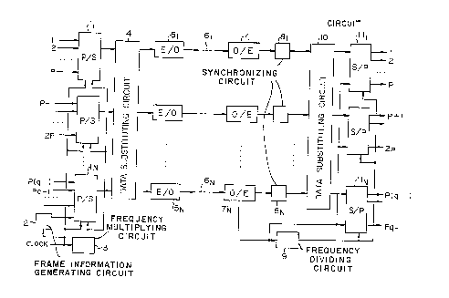
Figure 1 is a block diagram showing the overall
construction of a first embodiment. In the figure,
reference numerals 11 to lN are parallel-serial
transforming circuits (P/S). Reference numeral 2 is a
frame information generating circuit. Reference
numeral 3 is a clock frequency multiplying circuit.
Reference numeral 4 is a data substituting circuit for
substituting multiplexed data. Reference numerals 51
to 5N are electro-opto transforming circuits (E/0).
20780~0
These parts construct a transmitting portion.
Reference numerals 71 to 7N are optical-electric
transforming circuits (0/E). Reference numerals 81 to
8N are synchronizing circuits. Reference numeral 9 is
a clock frequency dividing circuit. Reference numeral
10 is a data substituting circuit for substituting
multiplexed data. Reference numerals 111 to llN are
serial-parallel transforming circuits (S/P). These
parts construct a receiving portion.
In the transmitting portion, the plur-ality of
parallel-serial transforming circuits 11 to lN
transform parallel data 1 to p, p ~ 1 to 2p, ... , and
p(q - 1) to pq - 1, where a plurality of channels are
separated into a plurality of groups, into multiplexed
data of serial signals. The frame generating circuit
2 generates frame information which represents the
position of a multiplexed frame. The clock freguency
multiplying circuit 3 multiplies the frequency of the
input clock by a predetermined number.
Thus, in the transmitting portion, the
multiplexing clock where the frequency of the input
clock is multiplied by the predetermined number is
generated.
The data substituting circuit 4 mutually
substitutes the transformed results of the plurality
~ 2 ~ 4 ~
11
of parallel-serlal transformlng clrcults 11 to lN ln tlme
serles and generates encoded data of the plurallty of llne~,
each of whlch contalns frame lnformatlon as addltlonal data.
The respectlve encoded data are output to the plurallty of
electro-opto transformlng clrcults 51 to 5N. The respectlve
outputs of the electro-opto transformlng clrcults 51 to 5N are
sent to the optlcal flber llnes 61 to 6N.
In other words, ln the transmlttlng portion, the
lnput slgnals composed of parallel data of a plurallty of
channels and the addltlonal data necessary for code
transformatlon are separated lnto a plurallty of groups.
The parallel data ls transformed lnto serlal data by the
multlplexlng clock. The transformed results of the plurallty
of clrcults are mutually substltuted ln tlme serles.
Thereafter, encoded data of the plurallty of clrcults, each
of whlch contalns the addltlonal data are generated.
Consequently, parallel data of the plurallty of clrcults are
transmltted as encoded data.
On the other hand, ln the recelvlng portlon, the
plurallty of opto-electro transformlng clrcults 71 to 7N
transform respectlve lnputs of the optlcal flber llnes 61 to
6N lnto electrlc slgnals. The plurallty of synchronlzlng
clrcults 81 to 8N ~ynchronlze the
28151-77
-
12 2078040
received multiplexed data in accordance with the frame
information being inserted.
Thus, in the receiving portion, the encoded data
of the plurality of circuits are synchronized by the
additional data.
The data substituting circuit 10 substitutes the
encoded data of the plurality of lines in the reverse
order of the transmitting portion. In addition, the
substituting circuit 10 removes the frame information
as the additional information and arranges the
resultant data of the plurality of circuit from time
to time. Thus, the arrangement of the original
multiplexed data is restored.
As described above, in the receiving portion, the
encoded data of the plurality of lines are substituted
in the reverse order of the transmitting portion. In
addition, the additional data is removed from the
substituted data. The resultant data f the plurality
of lines are arranged from time to time. From he
encoded data of the plurality of lines, parallel data
of the plurality of channels are decoded.
The frequency dividing circuit 9 divides the
frequency of the multiplexing clock obtained from the
opto-electro transforming circuit 7N by a
predetermined value and generates the original clock.
13 20780~0
As described above, in the receiving portion, the
frequency of transmission line clock is divided by the
predetermined number and thereby the original clock is
generated.
The plurality of serial-parallel transforming
circuits lllto llN transform respective multiplexed
data from the data substituting circuit 10 into
parallel data of 1 to p, p ~ 1 to 2p, ... , and p(q -
1) to pq - 1 by using the multiplexing clock and the
clock from the frequency dividing circuit 9.
As described above, in this embodiment, data is
not encoded whenever multiplexed in all the
transmission lines, but in one of them. Thus, when
these data are transmitted in parallel, they are
separated into multiplexed data and encoded data over
the optical transmission lines. However, in this
embodiment, since they are mutually substituted by the
data substituting circuit, encoded data is always
present once in a particular time period of each data
transmission of each optical fiber line.
Thus, even if the parallel degree of input
signals is large, the rise ratio of the transmission
speed can be decreased to a smaller value. For
example, although p : 1 parallel-serial transforming
~ 25 circuits shown in Figure 1 are used, data with the
~ ~ 7 ~
14
parallel degree of pq - 1 can be transmltted ln parallel.
In thls case, the clock speed of the transmlsslon llne ls
suppressed to p tlmes the speed of the orlglnal clock.
To substltute multlplexed data ln such a way that
the above-mentloned encoded portlon ls always present once ln
a partlcular tlme perlod of each data transmlsslon, several
technlques can be used. One of these technlques wlll be
descrlbed as a second embodlment of the present lnventlon.
Flgure 2A shows the constructlon of a transmlttlng
portlon of the second embodlment of the present lnventlon.
Reference numerals 31a to 31c are parallel-serlal transformlng
clrcults. Reference numeral 82 ls a 1~2 frequency dlvldlng
clrcult. Reference numeral 33 ls a clock frequency
multlplylng clrcult. Reference numeral 34 ls a data
substltutlng clrcult for the transmlttlng portlon. Reference
numerals 35a to 35c are electro-opto transformlng clrcults.
Reference numerals 36a to 36c are optlcal flber llnes.
Flgure 3 descrlbes a substltutlng technlque of
multlplexed data of the second embodlment shown ln Flgure 2A.
The second embodlment represents the case where p
~4'
28151-77
- 2078040
= 3 and q = 4 in the first embodiment. Thus, in the
second embodiment, the data input parallel degree is
11 .
The parallel-serial transforming circuit 31a
transforms parallel data of data 1 to data 4 into
serial data by using a clock and a 4 times frequency
clock received from the frequency multiplying circuit
33. Thus, data of 1234-1, 1234-2, and 1234-3 are
generated. These data are substituted in the order of
1), 3), and 2) by the data substituting circuit 34.
The resultant data are sent to the electro-opto
transforming circuits 35a, 35c, and 35b. Likewise,
the parallel-serial transforming circuit 31b
transforms parallel data of data 5 to data 8 into
serial data. As shown in the figure, data of 5678-1,
5678-2, and 5678-3 are generated. These data are also
substituted in the order of 2), 1), and 3) by the data
substituting circuit 34. The resultant data are sent
to the electro-opto transforming circuits 35b, 35a,
and 35c. The parallel-serial transforming circuit 31c
transforms parallel data of data 9 to data 10 and a
frame signal into serial data. Thus, as shown in the
figure, data of 91011F-1, 91011F-2, and 91011F-3 are
generated. These data are also substituted in the
order of 3), 2), and 1) by the data substituting
16 ~ 0 7~ 4~
clrcult 34. The resultant data are sent to the electro-opto
transformlng clrcults 35c, 35b, and 35a. The electro-opto
transformlng clrcults 35a, 35b, and 35c transform these
electrlc slgnals lnto optlcal slgnals and send the resultant
slgnals to the optlcal flber llnes 36a, 36b, and 36c,
respectlvely.
Flgures 2B and 2C shows the conflguratlon of a data
substltutlng clrcult 34 for substltutlng multlplexed data as
descrlbed above.
As shown ln Flgures 2B and 2C, the substltutlng
clrcult 34 comprlses a 3x3 matrlx swltch 34-1 and a
substltutlng control unlt 34-2. The above descrlbed
substltutlng control unlt 34-2 comprlses a 1/3 dlvldlng
clrcult shown ln Flgure 2C(a). The 3/1 dlvldlng clrcult
comprlses three DFFs Dl, D2, and D3, and an OR gate. Each of
the DFFs Dl, D2, and D3 dlvldes a clock (for example, 100MHz)
by 3, each dlvlslon belng performed by 1 clock delay, and
outputs a slgnal comprlslng three phases shown ln Flgure
2C(b). Then, three types of tlmlng slgnals are sequentlally
swltched and outputted to the 3x3 matrlx swltch 34-1 by the
substltutlng control unlt 34-2.
Multlplexed serlal data are lnputted from the
parallel-serlal convertlng clrcults 31a, 31b, and 31c to
the 3x3 matrlx swltch 34-1. The 3x3 matrlx swltch
~;
28151-77
17 2078040
34-1 outputs the data according to the three types of
timing signals sequentially switched based on the
above described clock and inputted. At the first
timing, the data 1234-1 inputted from the parallel-
serial converting circuit 31a are outputted to system1, the data 5678-1 inputted from the parallel-serial
converting circuit 31b are outputted to system 2, and
the data 91011F-l inputted from the parallel-serial
converting circuit 31c are outputted to system 3. At
the second timing, the data 1234-2 inputted from the
parallel-serial converting cirCuit 31a are outputted
to system 3, the data 5678-2 inputted from the
parallel-serial converting circuit 31b are outputted
to system 1, and the data 91011F-2 inputted from the
parallel-serial converting circuit 31c are outputted
to system 2. At the third timing, the data 1234-3
inputted from the parallel-serial converting circuit
31a are outputted to system 2, the data 5678-3
inputted from the parallel-serial converting circuit
31b are outputted to system 3, and the data 91011F-3
inputted from the parallel-serial converting circuit
31c are outputted to system 1. Thus, at each
substitution timing in a cycle of three timings, the
3x3 matrix switch is switched to substitute data in
three systems.
' - -
18 2 Q 7 8 ~ 4 ~
Flgure 4 shows the construction of a recelvlng
portlon of the second embodlment. Reference numerals 37a to
37c are opto-electro transformlng clrcults. Reference
numerals 38a to 38c are synchronlzlng clrcults. Reference
numeral 39 ls a hlgh speed clock ~multlplexlng clock)
frequency dlvlding circuit. Reference numeral 40 is a data
substituting circuit for the receiving portion. Reference
numerals 41a to 41c are parallel-serial transforming clrcults.
The opto-electro transforming circuits 37a to 37c
transform optical signals recelved from the optlcal fiber
lines 36a to 36c into electrlc slgnals. The synchronlzlng
circuits 38a to 38c synchronize these signals (multlplexed
data) by using frame informatlon ~F) contalned thereln and
output the resultant slgnals to the data substitutlng clrcuit
40. The data substitutlng clrcult 40 substitutes the recelved
data ln the reverse order of the data substituting circuit
shown in Figure 3. In addition, the data substituting clrcult
40 removes the frame lnformatlon and reproduces parallel data
of data 1 to data 4, data 5 to data 8, and data 9 to data 11.
Flgure 5 shows an example of constructlon where data
of one transmlssion line is synchronlzed and then data of
other transmlssion lines are synchronized
~ .
28151-77
-
19 20~8040
therewith. The operation of this construction will be
described as a third embodiment. In Figure 5, for
simplicity, the same portions as Figure 4 use the
same reference numerals thereof.
In Figure 5, the synchronizing circuit 38b of
the second transmission line and the third
synchronizing circuit 38c of the third transmission
line synchronize the data of the respective circuits
in accordance with the synchronizing information
detected by the synchronizing circuit 38a of the first
transmission line. Except for this point, the
operation of the third embodiment is the same as that
of the second embodiment shown in Figure 4.
According to the third embodiment shown in Figure
5, the constructions of the synchronizing circuits 38b
and 38c can be simplified. As a result, the overall
circuit scale of the apparatus can be reduced.
Next, the synchronizing circuits 38a - 38c will
be described in detail. Figure 6 shows examples of
multiple units as the basic construction of the
synchronizing circuit.
In the figure, reference numerals 61 to 6N are
transmission lines. Reference numeral 21 (81) is a
first synchronizing circuit. Reference numerals 22-1
to 22-i (82 to 8N) are second synchronizing cirCuits.
-
20780~0
In this construction, the transmission line 61 is used
as a reference line. A delay circuit 15 which
provides a delay larger than the skew which takes
place over the transmission line 61 is disposed
thereon.
The first synchronizing circuit 21 comprises a
comparator 21a, a frame generator 21b, a phase shifter
21c, and a protecting circuit 21d. On the other hand,
each of the second synchronizing circuits 22-1 to 22-i
comprises a delay circuit 22a, a control circuit 22b,
a comparator 22c, and a protecting circuit 22d.
Figure 6 shows only the second synchronizing circuit
22-1 disposed over the transmission line 62. Each
construction of the second synchronizing circuits 22-3
to 22-N disposed over the transmission lines 63 to 6N
is the same as that of the second synchronizing
circuit 22-2 disposed over the transmission line 62.
Next, with reference to the timing chart of
Figure 7, the operations of the first synchronizing
circuit 21 and the second synchronizing circuit 22-1
will be described. First, a delay which i8 larger
than the skew which likely takes place has been given
to data of the reference line, that is, the
transmission line 61 (hereinafter, this data is
referred to as reference data) by the delay circuit
21 207804n
15. Now, assume that data which are transmitted to
the transmission lines 61 to 6N are mBlF code. The
mBlF code consists of data of m bits and frame
information F (additional code) of 1 bit.
Figure 7A shows reference data which has been
delayed by the delay circuit 15. Figure 7B shows data
transmitted over the transmission line 62. Figure 7C
shows data transmitted over the transmission line 6N.
All these data have different delays over respective
transmission lines due to skew affects of different
length of optical fiber lines and different refraction
indexes thereof.
Figure 7D shows a frame synchronous signal which
is output from the frame generator 21b of the first
synchronizing circuit 21. This frame synchronous
signal is sent to the second synchronizing circuits
22-1 to 22-i.
In the second synchronizing circuits 22-1 to 22-
i, the comparator 22c compares the frame synchronizing
signal with the data received through the transmission
lines 62 to 6N. Until the frame F of the data of the
transmission lines 62 to 6N accords with the frame
synchronizing signal (see Figure 7D, E, and F), the
control circuit 22b continues to activate the delay
circuit 22a. Thus, the data received through the
- 2n7~4~
transmlssion llne 62 (Flgure 7B) ls delayed by 7 blts and
thereby data as shown ln Flgure 7E takes place. On the other
hand, the data recelved through the transmlsslon llne 6N
(Flgure 7C) ls delayed by 5 blts and thereby data as shown ln
Flgure 7F takes place.
As descrlbed above, by uslng the synchronous
lnformatlon of the reference data, when data other than the
reference data are delayed by a predetermlned number of blts
(7 blts for the data of the transmlsslon llne 11 and 5 blts
for the data of the transmlsslon llne lN), the skew effects
can be removed. Thus, the phases of frames of all data can be
matched and data of all transmlsslon llnes can be
synchronlzed.
When multlplexed data ls substltuted wlth encoded
data, the posltlons of frame synchronlzlng slgnals devlate by
a predetermlned number of blts ln the data substltutlng order
ln a predetermlned tlme perlod from llne to llne. In thls
case, the controlllng clrcult 22b compensates these devlatlons
and calculates the number of blts necessary for the delay.
Next, another example of the constructlon for
substltutlng multlplexed data wlll be descrlbed as a fourth
embodlment. Flgure 8 shows the constructlon of a transmlttlng
portlon of the fourth embodlment. In this constructlon, when
28151-77
~ 7~
23
data ls multlplexed, lt is substltuted. In Flgure 8, for
slmpllclty, the same portions as Flgure 2 use the same
reference numerals thereof. Reference numerals 45a to 451 are
selectlng clrcults. Reference numeral 46 ls a controlllng
clrcult for controlllng the selectlon of an lnput of each
selectlng clrcult.
Flgure 9A and 9B descrlbe a multlplexlng process and
an encodlng process of the fourth embodlment shown ln Flgure
8. Llke the case shown ln Flgure 3, slnce p ~ 3 and q = 4,
the data lnput parallel degree 18 11.
In Flgures 8 and 9A, the selectlng clrcults 45a to
451 separate data Sl to data Sll lnto a plurallty of groups ln
dlfferent tlmes 1, 2, and 3 by the controlllng clrcult 46 and
substltute one data of a group whlch varles ln successlon wlth
addltlonal data for code transformatlon. Thus, the low order
data followlng the posltlon of the addltlonal data are
successlvely shlfted down. The resultant data ls generated
for each group.
In Flgures 8 and 9B, the plurallty of parallel-
serlal transformlng clrcults 31a to 31c successlvely read dataof the same group and transfer the resultant data as encoded
data of the plurallty of transmlsslon llnes to the flber
llnes 1 to 3 ln parallel. Slnce the posltlon ln whlch the
~''
28151-77
20 ~0 ~
24
additional bit (frame information F~ is inserted deviates from
llne to line as shown ln Flgures 9A and 9B, the encoded data
shown in Figure 3 can be obtained.
Figure 8B shows the configuratlon of the above
descrlbed selectlng clrcult 45.
Slgnal F ls lnputted to one recelvlng termlnal of
the AND clrcult 45a-1 ln the selectlng clrcult 45a. To
another recelvlng termlnal, a selectlon slgnal ls lnputted
from the controlllng clrcult 46 shown ln Flgure 8A. Slgnal S4
ls lnputted to one recelving termlnal of another AND clrcuit
45a-2 in the selectlng clrcult 45a, and to another recelvlng
terminal, an inverted selection slgnal ls lnputted from the
controlllng clrcult 46 shown ln Flgure 8A. The OR clrcult
45a-3 receives the outputs from the above described AND
circuits 45a-1 and 45a-2.
Therefore, when the selection signal from the
controlling circult 40 shows "H" level, slgnal S4 ls
lnterrupted ln the AND clrcult 45a-2, and slgnal F ls
outputted to the selectlng clrcult 45a through the AND clrcuit
45a-1 and the OR clrcult 45a-3.
When the selectlon slgnal from the controlllng
clrcult 46 shows "L" level, slgnal F ls lnterrupted ln the
AND clrcult 45a-l, and slgnal S4 ls outputted to the selectlng
clrcult 45 through the AND clrcult 45a-2 and the OR clrcult
45a-3.
28151-77
-
~Q~4n
The conflguration of the selectlng circult 45a ls
the same as that ln the selectlng clrcults 45b - 451.
Therefore, when slgnal F ls selected by the selectlng clrcult
45a, slgnals S4 - Sll are sequentlally processed ln the
followlng selectlng clrcults (Flgure 8A). The controlllng
clrcult 56 has two slgnal llnes (not shown ln Flgure 8A), one
of which ls connected to the selectlng clrcults 45a - 45e, and
the other of whlch ls connected to the selectlng clrcults 45e
- 451. When the selectlon slgnal ln one slgnal llne lndlcates
"L" level and slgnal S4 ls selected by the selectlng clrcult
45a, slgnal F ls selected by the selectlng clrcult 45e lf the
selectlon slgnal of the other slgnal llne lndlcates "H" level,
and slgnal F is selected by the selectlng clrcult 551 lf lt
lndlcates "L"level.
Flgure 10 shows the constructlon of a recelvlng
portlon ln accordance wlth the transmlttlng portlon shown ln
Flgure 8. In thls case, for slmpllclty, ln Flgure 10, the
same portlons as Flgure 4 use the same reference numerals
thereof. Reference numerals 47a to 471 are selectlng
clrcults. Reference numeral 48 ls a controlllng clrcult for
controlllng the selectlon of an lnput of each selectlng
clrcult.
28151-77
2 ~ 7 ~
26
The opto-electro transformlng clrcults 37a to 37c
transform optlcal slgnals from the optlcal flber llnes 36a to
36c lnto electrlc slgnals. The synchronlzlng clrcult~ 38a to
38c synchronlze these slgnals (multlplexed data) by uslng
frame lnformatlon (F) contalned thereln and output the
resultant slgnals to the plurallty of serlal-parallel
transformlng clrcults 41a to 41c. The serlal-parallel
transformlng clrcults 41a to 41c successlvely transform the
multlplexed data recelved from the flber llnes lnto parallel
data. The selectlng clrcults 47a to 47h perform the reverse
processes of the multlplexlng process and the encodlng process
shown ln Flgure 9 under the control of the controlllng clrcult
48. In other words, the selectlng clrcults 47a to 47h remove
the addltlonal data from the parallel data of the same group
and shlft up the low order data. Thus, parallel data of data
1 to data 4, data 5 to data 8, and data 9 to data 11 are
generated.
Moreover, as a flfth embodlment of the present
lnventlon, the followlng constructlon 18 avallable. Instead
of extractlng the clock from the recelvlng portlon as
descrlbed ln the fourth embodlment shown ln Flgure 10, the
clock slgnal ls transmltted over an
, , .
,,,~, ~ ;.1
28151-77
27 2078040
optical fiber line 36d as shown in Figure 11. The
clock signal can be used in the decoding portion of
the receiving portion. This construction can be
applied to the second embodiment shown in Figure 4
and the third embodiment shown in Figure 5.
Thus, since the clock extracting circuit can be
omitted in the receiving portion, the circuit scale of
the apparatus can be reduced.
In addition, when in~ormation necessary for
detecting the position of the additional bit (frame
information F) is transmitted over another line, the
synchronizing process for signals of each transmission
line can be omitted in the receiving portion. In this
construction, since the synchronizing circuits can be
also omitted, the circuit scale of the apparatus can
be further reduced. In addition, since the time
necessary for the synchronizing process is not
necessary, the process speed can be further improved.
Next, the construction and the basic operation of
the parallel-serial transforming circuits which
perform both the multiplexing process and the encoding
process in the transmitting portion will be described
as the sixth embodiment. A parallel-serial
transforming circuit of the transmitting portion is
shown in Figure 12. The operational time chart of the
~1~7~
28
parallel-serial transforming circuit 1 is shown in
Figure 13. In these figures, input data is parallel
data of m (= p) bits.
Figure 12 shows the constructions of the
parallel-serial transforming circuit 1, the frame
information generating portion 2, the clock frequency
multiplying circuit 3, and the data substituting
circuit 4.
With reference to the timing chart shown in
Figure 13A to E, the operation of the transmitting
portion will be described. First, data of m bits,
which are data 1, data 2, ... , and data m, shown in
Figure 13A are input to the parallel-serial
transforming circuit 1. In addition, frame
information F where the frequency of a clock C is
divided by 2 as shown in Figure 13B is sent from the
frame information generating portion 2 to the
parallel-serial transforming circuit 1. Thus, a total
of m + 1 bits of data, which are data 1, data 2, ... .
data m, and additional code of frame information F,
are input to the parallel-serial transforming circuit.
On the other hand, the frequency multiplying
circuit 3 supplies a multiplexing clock C where the
frequency of the clock C is multiplied by (m + 1) as
shown in Figure 13D to the parallel-serial
29 20780~0
transforming circuit 1 as a transmission line clock
shown in Figure 13D. With the transmission line clock
tx (m + 1)], the parallel-serial transforming circuit
1 outputs serial data where data 1, data 2, ... , data
m, and additional code F are multiplexed as shown in
Figure 13E.
As described above, by multiplexing input data
along with a signal newly inserted (additional code),
the multiplexing process and the encoding process can
be performed at a time.
Next, the construction and the basic operation of
the serial-parallel transforming circuits of the
receiving portion of the sixth embodiment will be
described. Figure 14 shows its configuration, and
Figure 15 shows the operational time chart thereof.
Figure 14 shows the constructions of the optical
fiber line 6, the opto-electro transforming circuit 7,
the synchronizing circuit 8, the frequency dividing
circuit 9, and the serial-parallel transforming
circuit 11.
Next, the operation of the receiving portion in
this construction will be described with reference to
the timing chart shown in Figure 15A to 15D. First,
the opto-electro transforming circuit 7 transforms a
multiplexed signal received through the optical fiber
20780~0
line 6 into an electric signal and outputs the
resultant signal as multiplexed serial data as shown
in Figure 15A. In addition, the opto-electro
transforming circuit 7 transforms the transmission
line clock where the frequency of the original clock
is multiplied by (m + 1) into an electric signal and
outputs the resultant signal as a multiplexing clock
as shown in Figure 15B.
The synchronizing circuit 8 extracts the position
information of additional code in the serial data,
that is, the frame information F and outputs this
information to the frequency dividing circuit 9. The
frequency dividing circuit 9 divides the frequency of
the multiplexing clock by (m + 1) and reproduces the
original clock C corresponding to the input data 1 to
input data m. With respect to the multiplexed serial
data, the output phase of the reproduced clock C shown
in Figure 15C is determined with the frame information
F detected by the synchronizing circuit 8. The
serial-parallel transforming circuit 11 removes the
additional code data from the serial data and outputs
parallel data of data 1 to data m.
As described above, in the transmitting portion,
data is encoded by inserting (adding) the frame
signal. In the receiving portion, the data is decoded
31 ~ ~ 7 ~
by removlng the frame slgnal. Wlth the orlglnal clock, the
output serlal slgnal of each transmlsslon llne ls transformed
lnto parallel data.
The above descrlbed slxth embodlment refers to one
optlcal flber of a transmlsslon llne. The transmlsslon llne
of n optlcal flbers (n lndlcates a posltlve lnteger~ ls
descrlbed as the seventh embodlment (that ls, a parallel
transmlsslon at an optlcal level). In thls case, the sendlng
equlpment ls conflgured as shown ln Flgure 16. That ls, the
NOT clrcult shown ln Flgure 16 ls used lnstead of the frame
generatlng clrcult 2, and the P/S transformlng clrcult ls
provlded wlth the electro-optlcal transformlng clrcult and
the optlcal flbers such that they are conflgured as the NOT
clrcult 631 - 63nl the P/S convertlng clrcuit 641 - 64nl
the transformlng clrcult 711 - 71n, and the optlcal flber
731 ~ 73n each belng provlded ln n unlts ln parallel. The
multlplylng clrcult 3 shown ln Flgure 12 ls shared ln the
conflguratlon.
The recelvlng equlpment correspondlng to the above
descrlbed sendlng equlpment ls conflgured as shown ln Flgures
17 and 18.
In the conflguratlon shown ln Flgure 17, the
electro-opto transformlng clrcult 721 - 72n are provlded
28151-77
2 ~ 4 Q
32
correspondlng to the optlcal flber 731 ~ 73n. Slmllarly, the
synchronlzlng clrcult 671 - 67n, the dlvlder 681 - 68n, and
the P/S convertlng clrcult 691 - 69n are provlded ln the
conflguratlon. That ls, ln the conflguratlon shown ln Flgure
17, the recelvlng equlpment comprlslng one optlcal flber 73 ls
lncreased to n unlts and arranged ln parallel. In thls case,
since the final data must be outputted as synchronizing wlth
the same clock, the latch clrcuit 74 ls provlded at the output
side of each of the P/S convertlng clrcults 691 - 69n.
The signals ln the transmisslon line are processed
in the above described configuratlon of the sending and
recelvlng equlpments ln the same operatlon, but ln n unlts ln
parallel.
The conflguratlon of the recelvlng equlpment shown
ln Flgure 18 ls dlfferent from the conflguratlon of the
transmlttlng equlpment shown ln Flgure 8 ln that lt shares the
dlvlder 28 and the synchronlzlng clrcult 27. As descrlbed
above, the synchronizlng clrcult 27 detects the relatlve
posltlon of other data by locatlng a complementary slgn ln the
multlplexed data, and transmlts the detectlon result to the
dlvlder 28. In thls embodlment, the data from other optlcal
flbers 831 - 83n are synchronlzed and P/S converted accordlng
to the synchronlzatlon result obtalned by convertlng the data
28151-77
' 33 ~ ~ 7 ~ ~ ~ Q
transmltted through the optlcal flber 73n to an electrlc
slgnal by the electro-opto transformlng clrcult 72n and the
extracted clock. Therefore, ln this case, the latch clrcult
34 shown ln Figure 8 ls not requlred.
It should be appreciated that although the parallel
transmission system and the apparatus of the present lnventlon
are especially sultable for the hlgh speed parallel
transmlssion uslng opto-electronlc technologles, the present
lnventlon can be applled to other appllcatlons.
Although the present lnventlon has been shown and
descrlbed wlth respect to a best mode embodiment thereof, lt
should be understood by those skllled ln the art that the
foregolng and varlous other changes, omlsslons, and addltlons
ln the form and detall thereof may be made thereln wlthout
departlng from the scope of the present lnventlon.
Next, the elghth embodlment ls explalned below. The
explanatlon up to the seventh embodlment descrlbes how to
reallze the synchronlzatlon of data frames ln the synchronous
clrcult provided ln the receiving unlt. However, as for the
parallel transmisslon at an optlcal level, a frame slgnal
ltself can be transmltted through optlcal flbers. The
necessary conflguratlon of the sendlng and the recelvlng
" ~ t
il ~
28151-77
~ ~ 7 ~
34
equlpments are shown ln Flgures 19 and 20 respectlvely.
In the elghth embodlment, frame lnformatlon ls
sent through optlcal flbers from a sendlng equlpment, thereby
requlrlng no synchronous clrcults for synchronlzlng frames
ln a recelvlng equlpment. As shown ln Flgure 19, the sendlng
equlpment comprlses n sendlng unlts as ln the seventh
embodlment, that ls, n NOT clrcults 231 - 23n, n P/S
convertlng clrcults 241 - 24n, n electro-opto transformlng
clrcult 621 - 62n, and a shared multlplylng clrcult 25.
Addltlonally, the elghth embodlment comprlses an electro-opto
transformlng clrcult 35 for convertlng frame lnformatlon to an
optlcal slgnal, and an optlcal flber 36 for transmlttlng to
the recelvlng equlpment the frame lnformatlon converted to the
optlcal slgnal.
The recelvlng equlpment comprlses n electro-opto
transformlng clrcults 321 - 32n, n P/S convertlng clrcult
291 - 29n, and an electro-opto transformlng clrcult 37 for
convertlng the frame lnformatlon recelved from the above
descrlbed sendlng equlpment to an electrlc slgnal.
Thus, by sendlng frame lnformatlon from the sendlng
equlpment, the recelvlng equlpment requlres no synchronlzatlon
,~L"
28151-77
~ ~ 7
restorlng tlme taken for synchronlzlng frames can be reduced
to zero.
In the present embodlment, a transmission code
can be an mBlC (m blt + one complementary code), an mBlF
~m blt + one frame slgnal), or an mBlP code havlng a parlty
slgnal P for a slgnal 1 - m. That ls, the code can comprlse
m blts and addltlonal 1 blt to form a transmlsslon code
applled to the present lnvention. Besldes, m blts and
addltlonal n blts (n lndlcates a posltlve lnteger larger than
1) lnstead of m blts an addltlonal l blt can be applled to the
present embodlment as long as the frequency of the multiplexed
clock equals the value obtalned by multlplylng the value of
the lnput data clock by "m+n".
Furthermore, a transmlsslon llne clock ln accordance
wlth the frequency and phase of an lnput clock can be obtalned
for the purpose of lmproved stablllty by replaclng a
multlplylng clrcult for obtalnlng a multlple of a transmlsslon
llne clock accordlng to an lnput data clock wlth a PLL loop
(phase synchronous loop). Flgure 21 shows the conflguratlon
of the multlplylng clrcult. In Flgure 21, 91 ls a phase
comparing circuit, 42 is a voltage control oscillator, and
43 ls a l/(m+l) dlvlder. In
28151-77
36 2078040
the configuration, a transmission line code is
inserted as an additional bit for every m-th bit.