Note : Les descriptions sont présentées dans la langue officielle dans laquelle elles ont été soumises.
FJ-9442
1- 2078795
VOLTAGE STABILIZING CIRCUIT
BACKGROUND OF THE INVENTION
1~ Field of the Invention
The present invention relates to a voltage
stabilizing circuit, and more particularly to an output
voltage stabilizing circuit of a switching power supply
circuit used for, for example an electronic exchange
system.
Generally, in various electronic circuits, when
a power supply voltage fluctuates, the operating point of
a transistor or integrated circuit (CI) is changed so
that the originally intended performance cannot be
obtained. To prevent this, the output voltage of the
power supply circuit is detected by a voltage detecting
circuit, and when the detected voltage deviates from a
predete ;ned reference voltage, the power supply
circuit is controlled based on the deviation so as to
output a stable power supply voltage. The present
invention relates to a voltage stabilizing circuit for
the above case as an example.
(2) Description of a Prior Art
In a conventional voltage stabilizing circuit,
a voltage detecting circuit is realized by a mirror
circuit including two transistors arranged symmetrically.
With the mirror circuit, however, the relation between
the output voltage of the voltage stabilizing circuit and
the detected voltage detected by the voltage detecting
circuit depends on a base-emitter voltage of one of the
two transistors. The base-emitter voltage of the
transistor has a temperature characteristic such that the
base-emitter voltage fluctuates depending on the
temperature. Therefore, in the conventional voltage
stabilizing circuit, there is a problem in that the
accuracy of the detected output voltage is too low
because of the fluctuation of the base-emitter voltage
207879~
which may be caused when the temperature of the
environment for the voltage stabilizing circuit is
changed or when an abnormal accident occurs at the output
side of the power supply circuit to increase the
temperature.
It should be noted that such a problem is
generated in not only the case of the switching power
supply circuit explained above as an example of the
application of the voltage stabilizing circuit, but in a
series regulator that keeps the output voltage constant
by controlling a transistor or a variable resistor, or in
a voltage detecting circuit used in various other
electronic devices.
SUMMARY OF THE lNv~:NllON
Thus, the present invention has an object to provide
a voltage stabilizing circuit for stabilizing the output
voltage of an electronic device such as a switching power
supply circuit or a switching regulator in which a
voltage detecting circuit, for detecting the output
voltage of the voltage stabilizing circuit, as a control
voltage for the voltage stabilizing circuit can provide
the output voltage without being influenced by the
component of the base-emitter voltage BBE, SO that there
is no emitter-base voltage VBE in the relation between
the output voltage of the voltage stabilizing circuit and
a voltage detected by the voltage detecting circuit.
To attain the above object, there is provided,
according to the present invention, a voltage stabilizing
circuit for stabilizing an output voltage across the
output te_ ;nAls of an electronic device. The circuit
comprises a voltage detecting circuit, operatively
connected to the output terminals of the electronic
device, for detecting a control voltage in response to
the output voltage, and a control circuit, operatively
connected between the voltage detecting circuit and the
electronic device, for stabilizing, based on the control
~ 3 ~ 2078795
voltage, the output voltage of the electronic device.
The voltage detecting circuit includes a first series
circuit consisting of a first resistor and a first
transistor connected in series. The first transistor has
a first electrode connected through the first resistor to
one of the output terminal, a base electrode connected
to another one of the output t~ ; n~ ls, and a second
electrode. The voltage detecting circuit further
includes a second series circuit consisting of a second
resistor and a second transistor connected in series.
The second transistor is connected to function as a diode
and has a third electrode connected through the second
resistor to the second electrode of the first transistor.
The control voltage is obtained across the second series
lS circuit. The first resistor and the second resistor have
substantially the same resistances, whereby the control
voltage is made to be substantially the same as the
output voltage.
In the above voltage stabilizing circuit, the first
transistor and the second transistor are PNP transistors,
and the first electrode of the first transistor is an
emitter, the third electrode of the second transistor is
an emitter, and the emitter-base voltage of the first
transistor is substantially the same as the emitter-base
voltage of the second transistor.
Alternatively, the first transistor and the second
transistor may be NPN transistors.
In the above voltage stabilizing circuit, the
electronic device is a switching power supply circuit,
and the control circuit controls, in response to the
control voltage, an ON and OFF period of an input voltage
applied to the switching power supply circuit.
Instead of the second transistor, a diode may
alternatively be employed.
According to the above constitution of the present
invention, since the detected control voltage does not
include the component of the base-emitter voltage of the
~ - 4 -
2078795
transistor, the output voltage is not greatly influenced
by temperature.
BRIEF DESCRIPTION OF TXE DRAWINGS
The above object and features of the present
invention will be understood more clearly from the
following description of the preferred embodiments with
reference to the accompanying drawings, wherein:
Figure 1 is a circuit diagram of a conventional
voltage stabilizing circuit;
Fig. 2 is a circuit diagram of a voltage stabilizing
circuit according to an embodiment of the present
invention;
Fig. 3 is a circuit diagram of a voltage stabilizing
circuit for stabilizing an output voltage of a switching
power supply circuit, according to another embodiment of
the present invention;
Fig. 4 to Fig. 7 are circuit diagrams of
conventional switching power supply circuits;
Fig. 8 is a circuit diagram of a voltage stabilizing
circuit according to still another embodiment of the
present invention;
Fig. 9 is a circuit diagram of a voltage stabilizing
circuit according to still another embodiment of the
present invention; and
Fig. 10 is a circuit diagram of a voltage
stabilizing circuit according to still another embodiment
of the present invention.
DESCRIPTION OF PREFERRED EMBODIMENTS
For better understanding of the present invention, a
conventional output voltage stabilizing circuit of a
switching power supply circuit is first described with
reference to Fig. 1. In Fig. 1, 31 is a switching power
supply circuit, 32 and 33 are input term;n~ls of the
switching power supply circuit, 34 is a voltage detecting
circuit, 35 and 36 are output terminals of the switching
power supply circuit, 37 is a battery for producing a
~ 5 ~ 2078795
reference voltage Vref for c~ ~rison, 38 is an error
amplifier, 39 is a pulse width control comparator for
comparing the control voltage detected by the voltage
detecting circuit 34 and a reference voltage Vr~f, 40 is a
transistor, 41 is a transistor connected to function as a
diode, and 42 to 45 are resistors.
Here, the transistors 40 and 41 constitute a mirror
circuit in which currents Il and I2 flowing through the
transistors have substantially the same values.
Generally, the ground potential at the output
te in~l 36 of the switching power supply circuit 31 is
not always the same as the ground potential at the input
te in~l 33 thereof. Therefore, the voltage detecting
circuit 34 is necessary to detect a control voltage Vr.
The voltage Vr is dete ined with respect to the ground
potential at the input te in~l 33 of the switching power
supply circuit 31, whereas the output voltage V3 iS
dete i~e~ with respect to the ground potential at the
output t~ in~1 36. The control voltage Vr is used to
control the input side of the switching power supply
circuit 31.
The voltage detecting circuit 34 is constructed by a
mirror circuit comprising the transistors 40 and 41, and
the resistor 45 connected to the collector side of the
transistor 40. The control voltage Vr across the
te_ inals of the resistor 45 is detected when a collector
current I2, which is nearly equal to the emitter current,
flows through the transistor 40.
The relation between the detected control voltage Vr
across the ends of the resistor 45 and the output
voltage V3 of the switching power supply circuit 31 can
be determined as follows.
Since 1/hpE = 0,
the following is established:
I~ = (V3 - VD)/(R43 + R44)
V2 = I~-R43 + VD
:
:
:
207879~
I2 = (V2- VBE)/R42
Vr = I2'R45~
Assuming that VD = V~S, then
V3 = Vr(R42/R45) ( 1 ~ R44/R43) + VBE ... (1)
The above symbols are defined as follows.
hF~: a direct current amplification factor of the
transistor 40,
V2: a potential difference between the output
terminal 35 and the base of the diode-connected
transistor 41,
V~: a forward voltage of the diode-connected
transistor 41,
VBE: a base-emitter voltage of the transistor 40,
I1: a current of the diode-connected transistor 41,
I2: a collector current of the transistor 40 nearly
equal to the emitter current, and
R42 - R45: values of the resistors 42 to 45.
The difference between the detected voltage Vr and
the reference voltage Vref, is amplified by the error
amplifier 38. The output of the error amplifier 38 is
supplied to the pulse width control comparator 39. The
ratio of the ON period and the OFF period of the
switching transistor Q1 is changed depending on the
output of the pulse width control comparator 39, whereby
the output voltage V3 of the switching power supply
circuit 31 is stabilized.
Methods of controlling an ON/OFF state of the
transistor Ql are: pulse number modulation in which one
of the ON period and the OFF period of the transistor Q
is kept constant and the other is changed, and pulse
width modulation in which the duty cycle is made constant
and the ratio between the ON period and the OFF period of
the transistor Ql (the duty ratio of the ON/OFF control
pulse signal) is changed.
In the conventional equation (1) representing the
relation between the output voltage V3 and the detected
~ 7 ~ 207879~
voltage Vr/ there is a component of the base-emitter
voltage V3E. The base-emitter voltage B3E of the
transistor 40 has a temperature characteristic in which
the base-emitter voltage of the transistor 40 changes
depending on the temperature. Therefore, there is a
problem in that the accuracy of the detection of output
voltage is lowered depending on the temperature
fluctuation caused by a change of the operating
enviLo~- ?nt or an abnormality in the output side of the
power supply circuit.
It should be noted that such a problem is generated
in not only the case of the switching power supply
circuit explained above as an example of the application
of the voltage stabilizing circuit, but also in a series
regulator for keeping the output voltage constant by
controlling a transistor or a variable resistor, or in a
voltage stabilizing circuit used in various other
electronic devices.
Thus, the present invention has an object to provide
a voltage stabilizing circuit for stabilizing an output
voltage of an electronic device in which a voltage
detecting circuit has a special construction for
cancelling the component of the base-emitter voltage V3E
in the related equation between the output voltage V3,
which is to be detected, and the control voltage Vrr so
that a predet~ ined accuracy with respect to the output
voltage can be kept even when a temperature fluctuation
occurs.
Embodiments of the present invention will be
described in the following.
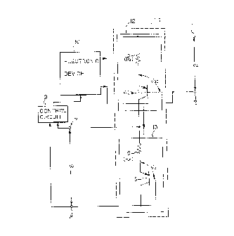
Figure 2 is a circuit diagram of a voltage
stabilizing circuit according to an embodiment of the
present invention. In Fig. 2, the voltage stabilizing
circuit includes an electronic device 10 for generating
an output voltage V3 which is applied across output
terminals 1 and 2, a voltage detecting circuit 11 for
' '
" , . ~
,: ,: .:
,, : ; .. , , ;' ~
.. , ~ .,
- 8 - 2078795
detecting a control voltage Vrl and a control circuit 9
for controlling the electronic device lO based on the
control voltage Vr. To the output terminals 1 and 2, a
load (not shown) is connected. The voltage detecting
S circuit 11 includes a first series circuit 12 and a
second series circuit 13. The first series circuit 12
includes a first resistor 3 and a first PNP transistor 4
connected in series. The second series circuit 13
includes a second resistor 5, and a second PNP
transistor 6 connected in series. The first series
circuit 12 and the second series circuit 13 are connected
to each other in series. Namely, the collector of the
first PNP transistor 4 is connected through the second
resistor 5 to the emitter of the second PNP transistor 6.
The first resistor 3 is connected between the output
t~ i n~l l and the emitter of the PNP transistor 4. The
base of the first PNP transistor 4 is connected to the
output te_ in~l 2. The second resistor 5 is connected
between the collector of the first PNP transistor 4 and
the emitter of the second PNP transistor 6. The second
PNP transistor 6 is connected to function as a diode.
Namely, the base and the collector of the second PNP
transistor 6 are connected together. The control
voltage Vr is detected across the ends of the second
series circuit 13. Namely, the emitter of the second
transistor 6 is connected through the second resistor 5
to a first control t~rri n~l 7, and the collector of the
second transistor 6 is connected to a second control
termin~l 8. The control voltage Vr is detected between
the first and the second control ter~in~ls 7 and 8.
The control voltage Vr is applied to the control
circuit 9. In response to the control voltage Vrr the
control circuit 9 controls the electronic device 10 so
that the output voltage V3 iS stabilized.
Here, instead of the PNP transistors 4 and 6, PNP
transistors may alternatively be employed. Further,
'~'' .
..
- 9 - 207879~
instead of the PNP transistor 6, a conventional diode may
alternatively be employed. Further, instead of the
second series circuit 13, the emitter of the second PNP
transistor 6 may be directly connected to the collector
of the first transistor 4. In this case, the base and
the collector of the second PNP transistor 6 may be
connected through the second resistor 5 to the second
control t~ inal 8.
In the voltage stabilizing circuit shown in Fig. 2,
the equation showing the relationship between the
detected control voltage Vr and the output voltage V3 iS
as follows.
Since 1/hpE = 0,
the following is established.
I = (V3 - VD) tR1
Vr = I ~ R2 + VD
Assuming that VD = V~E, then
V3 = (Rl/R2)VR + VRE(1 - Rl/R2) ... (2)
can be derived.
The above symbols are defined as follows:
hpE: a direct current amplification factor of the
first PNP transistor 4,
Rl: the resistance of the first resistor 3
R2: the resistance of the second resistor 5
VD: a forward voltage of the second PNP
transistor 6 in a diode connection,
V~E: a base-emitter voltage of the first PNP
transistor 4, and
I: a current flowing through the PNP transistors 4
and 6.
Namely, the equation representing the relation
between the detected control voltage Vr and the output
voltage V3 iS expressed by the equation (2), in which, by
making the values of the Rl and R2 substantially the
same, the component of the base-emitter voltage V~E/
which changes depending on the temperature while the
.
lO- 2078795
transistor is being used, can be omitted. The
equation (2) thus becomes:
V3 = Vr
Accordingly, even when the base-emitter voltage of
the transistor 4 is changed depending on a change of the
temperature of the environment in which the transistor 4
is used, the detected control voltage Vr is substantially
the same as the output voltage without being influenced
by the change of the temperature.
Fig. 3 is an embodiment in which the voltage
stabilizing circuit of the present invention is applied
to a switching power supply circuit, wherein 21 is a
switching powe~ supply circuit, 11 is the voltage
detecting circuit shown in Fig. 2, 23 and 24 are input
te in~ls of the switching power supply circuit 21, 25
and 26 are output t~rmin~ls of the switching power supply
circuit 21, 27 is a battery for producing a comparison
reference voltage Vref, 28 is an error amplifier, and 29
is a pulse width control comparator. The switching power
supply circuit 21 is an example of the electronic
device 10 shown in Fig. 2. The battery 28 and the pulse
width control comparator 29 constitute an example of the
control circuit 9 shown in Fig. 2.
Here, the comparison reference voltage Vref in
Fig. 3, the error amplifier 28, and the pulse width
control comparator 29 have the same functions as the
comparison reference voltage Vref in Fig. 1, the error
amplifier 38, and the pulse width control comparator 39
in the conventional voltage stabilizing circuit shown in
Fig. 1. The ON/OFF control of the switching power supply
circuit 21 is the same as the switching power supply
circuit 31 shown in Fig. 1.
As the switching power supply circuit 21, there is a
forward type as shown in Fig. 4 or a fly-back type as
shown in Fig. 5, in which an input and an output are
isolated from each other, and a step down type as shown
11 207879~
in Fig. 6 or a step up type as shown in Fig. 7, in which
an input and an output are not isolated from each other.
In any case, by controlling a transistor Ql to be turned
ON or OFF, an input voltage Vl is converted into an
output voltage VO.
Referring back to Fig. 3, the difference between the
detected voltage Vr and the reference voltageref is
amplified by the error amplifier 28. The output of the
error amplifier 28 is supplied to the pulse width control
comparator 29. The ratio of the ON period and the OFF
period of the switching transistor Ql is changed
depending on the output of the pulse width control
comparator 29, whereby the output voltage V3 of the
switching power supply circuit 31 is stabilized.
Methods of controlling an ON/OFF state of the
transistor Ql are: a pulse number modulation in which one
of the ON period and the OFF period of the transistor Q
is kept constant and the other is changed, and a pulse
width modulation in which the cycle is made constant and
the ratio between the ON period and the OFF period of the
transistor Ql (the duty ratio of the ON/OFF control pulse
signal) is changed. The output voltage of the step down
type increases in proportion with the rate of the ON time
of the transistor Ql. The output voltage of the
transistor Ql increases in proportion to the square of
the rate of the ON time of the transistor Ql.
Figure 8 is a circuit diagram of a voltage
stabilizing circuit applied to a switching power supply
circuit, according to another embodiment of the present
invention.
The only difference between Fig. 3 and Fig. 8 is
that, instead of the PNP transistors 4 and 6 in Fig. 3,
NPN transistors 4a and 6a are employed in a voltage
detecting circuit lla. The voltage detecting circuit lla
consists of a first circuit 12a and a second circuit 13a.
The first circuit 12a includes the NPN transistor 4a and
.
.
'''' '
.,
207879~
~ 12 -
the resistor 3. The second circuit 13a includes the NPN
transistor 6a and the resistor 5. The collector of the
NPN transistor 4a is connected to an input of the
comparator 28. The base of the NPN transistor 4a is
connected through the resistor 3 to the output
t~r~in~l 25. The emitter of the NPN transistor 4a is
connected to the output te inal 26. The NPN
transistor 6a is connected to function as a diode.
Namely, the collector and the base of the NPN
transistor 6a are connected together to the input
t~ i n~l 23 of the switching power supply circuit 21.
The emitter of the NPN transistor 6a is connected trhough
the resistor 5 to the collector of the NPN transistor 4a.
By this construction, the same effect as that
provided by the circuit in Fig. 3 can be obtained.
Figure 9 is a circuit diagram of a voltage
stabilizing circuit applied to a switching power supply
circuit, according to still another embodiment of the
present invention. The Fig. 9, a voltage detecting
circuit llb consists of a first series circuit 12b and a
second series circuit 13b. The first series circuit 12b
is the same as the first series circuit 12 in Fig. 3.
The only difference between Fig. 3 and Fig. 9 is
that, instead of the PNP transistor 6 in Fig. 3, a
diode 6b is employed in the second series circuit 13b.
The anode of the diode 6b is connected through the
resistor 5 to the collector of the PNP transistor 4. The
cathode of the diode 6b is connected to the input
te ; n~ l 24.
By this construction also, the same effect as that
in Fig. 3 can be obtained.
Fiqure 10 is a circuit diagram of a voltage
stabilizing circuit according to still another embodiment
of the present invention. In ~ig. 10, a voltage
detecting circuit llc consists of a first series
circuit 12c and a second series circuit 13c. The first
series circuit 12c is the same as the first series
- 13 - 2 ~ 7 8 7 9 ~
circuit 12 in Fig. 3.
The only difference between Fig. 3 and Fig. 10 is
that, in Fig. 10, the emitter of the PNP transistor 6 in
the second series circuit 13c is directly connected to
the collector of the PNP transistor 4, and the collector
of the PNP transistor 6 is connected through the
resistor 5 to the negative electrode of the battery 27.
In the circuit of Fig. 10 also, the transistor 6 may be
replaced by a diode.
By this construction also, the same effect as that
provided by the circuit in Fig. 3 can be obtained.
From the foregoing description, it is apparent that,
according to the present invention, the voltage
stabilizing circuit has a construction in which the
component of the base-emitter voltage VBE of a transistor
in the voltage detecting circuit can be omitted from the
related equation between the output voltage to be
stabilized and a control voltage for controlling the
voltage stabilizing circuit. Therefore, even when the
temperature fluctuates, fluctuation of the detected
control voltage is not caused so that the accuracy of the
output voltage can be increased. Further, in comparison
with the conventional voltage stabilizing circuit using
the mirror circuit, the number of resistors to be used
can be decreased in the voltage detecting circuit of the
present invention so that space efficiency when the
circuit is mounted in various electronic devices can be
improved or a cost decrease can be attained.