Sélection de la langue

Search

Sommaire du brevet 2079292 

Énoncé de désistement de responsabilité concernant l'information provenant de tiers

Une partie des informations de ce site Web a été fournie par des sources externes. Le gouvernement du Canada n'assume aucune responsabilité concernant la précision, l'actualité ou la fiabilité des informations fournies par les sources externes. Les utilisateurs qui désirent employer cette information devraient consulter directement la source des informations. Le contenu fourni par les sources externes n'est pas assujetti aux exigences sur les langues officielles, la protection des renseignements personnels et l'accessibilité.

Disponibilité de l'Abrégé et des Revendications

L'apparition de différences dans le texte et l'image des Revendications et de l'Abrégé dépend du moment auquel le document est publié. Les textes des Revendications et de l'Abrégé sont affichés :

  • lorsque la demande peut être examinée par le public;
  • lorsque le brevet est émis (délivrance).
(12) Brevet: (11) CA 2079292
(54) Titre français: RECEPTEUR DE FILTRE ADAPTE A REPONSE RAPIDE MUNI D'UN EGALISEUR RECURSIF
(54) Titre anglais: FAST RESPONSE MATCHED FILTER RECEIVER WITH DECISION FEEDBACK EQUALIZER
Statut: Réputé périmé
Données bibliographiques
(51) Classification internationale des brevets (CIB):
  • H04B 1/10 (2006.01)
  • H04L 25/03 (2006.01)
(72) Inventeurs :
  • YAMAMOTO, TAKESHI (Japon)
(73) Titulaires :
  • NEC CORPORATION (Japon)
(71) Demandeurs :
(74) Agent: SMART & BIGGAR
(74) Co-agent:
(45) Délivré: 1996-11-12
(22) Date de dépôt: 1992-09-28
(41) Mise à la disponibilité du public: 1993-03-28
Requête d'examen: 1992-09-28
Licence disponible: S.O.
(25) Langue des documents déposés: Anglais

Traité de coopération en matière de brevets (PCT): Non

(30) Données de priorité de la demande:
Numéro de la demande Pays / territoire Date
3-248192 Japon 1991-09-27

Abrégés

Abrégé anglais


A tap-weight controller of a matched filter includes a tapped delay line
having a series of delay elements for receiving an incoming digital signal to
produce successively delayed signals at successive taps of the delay line
so that the signal at the center tap coincides with the output of a decision
feedback equalizer (DFE). Correlation circuits are provided corresponding
respectively to tap-weight multipliers of a transversal filter and to the taps
of the delay line of the tap-weight controller. In each correlation circuit,
correlation is detected between the output of the DFE and a signal from
the corresponding tap of the delay line, and a signal indicating the
detected correlation is integrated over a prescribed interval. An adder has
a first input for receiving the detected correlation signal and a second input
for receiving the integrated signal or a tap-weight control signal to produce
a summed signal. The correlation signal is delayed for an interval equal to
the prescribed interval and subtracted from the summed signal to produce
an output which is applied to the adder as the tap weight control signal as
well as to the corresponding tap-weight multiplier. The integrated signal is
initially applied to the second input of the adder, and thereafter, the tap-
weight control signal is applied to the adder to update the control signal at
symbol intervals.

Revendications

Note : Les revendications sont présentées dans la langue officielle dans laquelle elles ont été soumises.


- 8 -

What is claimed is:

1. A matched filter receiver in combination with a decision feedback
equalizer, comprising:
a transversal filter having a tapped delay line for receiving an incoming
digital signal to produce successively delayed signals at successive taps of
the delay line, a plurality of tap-weight multipliers connected respectively
to the successive taps of said delay line, and means for summing output
signals of said tap-weight multipliers to produce a filter output, and
supplying the filter output to said decision feedback equalizer;
a second tapped delay line having a series of delay elements for
receiving said incoming digital signal to produce successively delayed
signals at successive taps of the second delay line so that the delayed
signal at a center tap of the second delay line is time coincident with an
output signal from said decision feedback equalizer;
a plurality of correlation circuits corresponding respectively to the tap-
weight multipliers of said transversal filter and the successive taps of the
second delay line, each of the correlation circuits comprising:
a correlation detector for detecting a correlation between the output
signal of said decision feedback equalizer and a signal from the
corresponding tap of said second tapped delay line to produce a
correlation output signal;
integrator means for integrating said correlation output signal over a
prescribed interval to produce an integrated signal;
an adder having a first input terminal receiving said correlation output
signal, and a second input terminal;
delay means for delaying said correlation output signal for an interval
equal to said prescribed interval to produce a delayed signal;
a subtractor for detecting a difference between said delayed signal
and an output signal of said adder to produce a difference signal and

- 9 -

supplying the difference signal to the corresponding tap-weight multiplier;
and
means for initially coupling said integrated signal to the second input
terminal of said adder and subsequently coupling said difference signal to
said second input of the adder, instead of said integrated signal.

2. A matched filter receiver for a demodulator, comprising:
a decision feedback equalizer;
means for generating an out-of-sync signal when the demodulator is
not synchronized with an incoming signal;
a transversal filter having a tapped delay line for receiving a signal
from said demodulator to produce successively delayed signals at
successive taps of the delay line, a plurality of tap-weight multipliers
connected respectively to the successive taps of said delay line, and means
for summing output signals of said tap-weight multipliers to produce a filter
output, and supplying the filter output to said decision feedback equalizer;
a second tapped delay line having a series of delay elements
connected to receive said incoming digital signal to produce successively
delayed signals at successive taps of the second delay line so that the
delayed signal at a center tap of the second delay line is time coincident
with an output signal from said decision feedback equalizer;
a plurality of correlation circuits corresponding respectively to the tap-
weight multipliers of said transversal filter and the successive taps of the
second delay line, each of the correlation circuits comprising:
a correlation detector for detecting a correlation between the output
signal of said decision feedback equalizer and a signal from the
corresponding tap of said second tapped delay line to produce a
correlation output signal;
a resettable integrator, when enabled, for integrating said correlation
output signal;


- 10 -

an adder having a first input receiving an output signal from said
correlation detector and a second input;
delay means for delaying the output signal of said correlation detector
for a prescribed interval;
a subtractor for detecting a difference between output signals of said
adder and said delay means to produce a difference signal and supplying
the difference signal to the corresponding tap-weight multiplier; and
control means responsive to said out-of-sync signal for resetting said
integrator and responsive to absence of said out-of-sync signal for
enabling said integrator to integrate said correlation output signal over an
interval equal to said prescribed interval to produce an integrated signal,
coupling said integrated signal to the second input of said adder, and
subsequently coupling said difference signal to said second input of said
adder, instead of said integrated signal.

3. A matched filter receiver for a demodulator having means for
generating an out-of-sync signal when the demodulator is not
synchronized with an incoming signal, comprising:
a decision feedback equalizer;
a transversal filter having a tapped delay line for receiving an incoming
digital signal to produce successively delayed signals at successive taps of
the delay line, a plurality of tap-weight multipliers connected respectively
to the successive taps of said delay line, and means for summing output
signals of said tap-weight multipliers to produce a filter output, and
supplying the filter output to said decision feedback equalizer;
a second tapped delay line having a series of delay elements
connected to receive said incoming digital signal to produce successively
delayed signals at successive taps of the second delay line so that the
delayed signal at a center tap of the second delay line is time coincident
with an output signal from said decision feedback equalizer;


- 11 -
a plurality of correlation circuits corresponding respectively to the tap-
weight multipliers of said transversal filter and the successive taps of the
second delay line, each of said correlation circuits comprising:
a correlation detector for detecting a correlation between the output
signal of said decision feedback equalizer and a signal from the
corresponding tap of said second tapped-delay line;
a resettable integrator, when enabled, for integrating a signal from said
correlation detector;
one-symbol delay means for delaying an output signal of said
integrator for a symbol interval;
a selector having a first input terminal connected to the output of said
one-symbol delay means, a second input terminal, and an output terminal
for selectively establishing a first connection between said first input
terminal and said output terminal, or a second connection between said
second input terminal and said output terminal;
a resettable adder, when enabled, for summing output signals from
said selector and said correlation detector;
L-symbol delay means for delaying a signal from said correlation
detector for an L-symbol interval;
a resettable subtractor, when enabled, for subtracting the output of
said L-symbol delay means from the output of said resettable adder to
produce a difference signal and supplying the difference signal to the
second input of said selector and to the corresponding tap-weight
multiplier;
first resetting means responsive to said out-of-sync signal for resetting
said integrator and responsive to absence of said out-of-sync signal for
enabling said integrator;
second resetting means for resetting said resettable adder and
subtractor an L -symbol interval after said integrator is reset by said first
resetting means and enabling said resettable adder and resettable


- 12 -

subtractor an L-symbol interval after said integrator is enabled; and
control means for initially causing said selector to establish said first
connection and subsequently causing said selector to establish said second
connection an (L+1)-symbol interval after said integrator is enabled by said
first resetting means.

Description

Note : Les descriptions sont présentées dans la langue officielle dans laquelle elles ont été soumises.


NE-462
2079292

TITLE OF THE INVENTION
2 "Fast Response Matched Filter Receiver With Decision Feedback Equalizer"
3 BACKGROUND OF THE INVENTION
4 The present invention relates generally to equalization techniques for
s digital modulation such as QAM (quadrature amplitude modulation), and
6 more specifically to a matched filter receiver used in combination with a
7 decision feedback equalizer.
8 In digital radio transmission systems, intersymbol interference can be
9 equalized using a decision feedback equalizer if the ratio of undesired-to-
desired signal (p) is smaller than 1. However, if the desired, direct signal
11 arrives at a receiver later than a undesired, reflected version of the
12 transmitted signal, interference occurs between them, causing what is
13 called multipath fading. When this occurs, the amplitude of the undesired
14 signal is stronger than the desired signal, hence p > 1, giving rise to a large
negative peak at time t = -T (where T is the symbol timing) with respect to
16 the center, positive peak at the origin of the impulse response of the
17 transmission system, whereas, when p= 0, i.e., in the absence of the
18 undesired component, the impulse response is symmetrical with respect to
19 the origin. Under such circumstances, intersymbol interference cannot
completely be equalized.
21 It is known that the transfer function of an optimum filter is the complex
22 conjugate of the spectrum of the input signal and such a filter is called a
23 matched filter. Since the impulse response of the matched filter is a time-
24 reversed and delayed version of the input signal, the application of a signal
2 5 whose U/D ratio is smaller than 1 to the matched filter results in the
2 6 generation of two negative peaks, one at time t = -T and the other at t = T,
27 both having amplitudes one-half of the amplitude of the original negative
2 8 peak at time t = -T.
29 A proposal has been made for using a matched filter in combination
3 0 with a decision feedback equalizer in order to take advantage of the *

N E-462

-2- 2079292

unique characteristic of the matched filter for equalizing signals affected by
2 multipath fading since the two negative peaks at the output of the
3 matched filter can be easily equalized by the decision feedback equalizer.
4 More specifically, the matched filter is implemented with a transversal filter5 and a tap-weight controller to control the tap weights of the transversal
6 filter in an adaptive fashion in response to the output of the decision
7 feedback equalizer. The tap-weight controller comprises a plurality of
8 correlation circuits corresponding respectively to the tap-weight multipliers
9 of the transversal filter to detect correlations between delayed incoming
10 signals with the output of the decision feedback equalizer. In each
11 correlation circuit, the detected correlation is integrated over a period L x T
12 and divided over time L to produce a tap-weight control signal which is an
13 average value of the integrated signal. Since this control signal is updated
14 at L x T intervals, the prior art matched filter cannot equalize signals
15 affected by multipath fading which varies at rates higher than the rate at
16 which the output of the matched filter is updated.
1 7 SUMMARY OF THE INVENTION
18 It is therefore an object of the present invention to provide a matched
19 filter receiver capable of tracking high speed variations of signals affected2 0 by multipath fading.
21 According to the present invention, the matched filter receiver
22 comprises a transversal filter having a tapped delay line for receiving an
23 incoming digital signal to produce successively delayed signals at
24 successive taps of the delay line, a plurality of tap-weight multipliers
25 connected respectively to the successive taps of the delay line, and means
26 for summing output signals of the tap-weight multipliers to produce a filter
27 output, and supplying the filter output to a decision feedback equalizer. A
28 tap-weight controller includes a second tapped delay line having a series
29 of delay elements for receiving the incoming digital signal to produce
3 0 successively delayed signals at successive taps of the second delay line so

N E-462
3 2079292

that the delayed signal at a center tap of the second delay line is time
2 coincident with an output signal from the decision feedback equalizer. A
3 plurality of correlation circuits are provided corresponding respectively to
4 the tap-weight multipliers of the transversal filter and the successive taps of
the second delay line. Each of the correlation circuits comprises a
6 correlation detector for detecting a correlation between the output signal7 of the decision feedback equalizer and a signal from the corresponding
8 tap of the second tapped delay line to produce a correlation output signal,
g an integrator for integrating the correlation output signal over a prescribed
interval to produce an integrated signal, and an adder having a first input
11 terminal receiving the correlation output signal, and a second input
12 terminal. Delay means is provided for delaying the correlation output
13 signal for an interval equal to the prescribed interval to produce a delayed
14 signal. A subtractor detects the difference between the delayed signal andan output signal from the adder to produce a difference signal for coupling
16 to the corresponding tap-weight multiplier as a tap-weight control signal.17 The integrated signal is initially applied to the second input terminal of the
18 adder, and thereafter, the difference signal (tap-weight control signal) is
19 applied to it, instead of the integrated signal. As a result, the tap-weight
output signal is summed with a new correlation output signal and the old
21 correlation output signal is then removed from the control signal by
22 subtractor. As the process continues, the tap weight control signal is
23 repeatedly updated at symbol intervals.
24 BRIEF DESCRIPTION OF THE DRAWINGS
The present invention will be described in further detail with reference
26 to the accompanying drawings, in which:
27 Fig. 1 is a block diagram of a matched filter receiver with a decision
28 feedback equalizer; and
2 9 Fig. 2 is a block diagram of each correlation circuit of Fig. 1.

NE-462
2079292

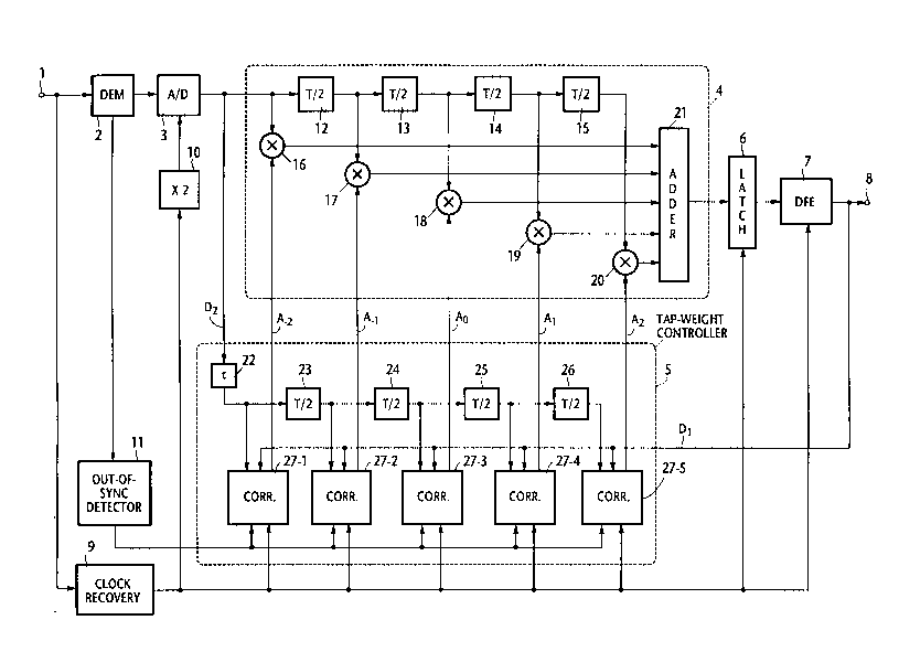
DETAILED DESCRIPTION
2 Referring to Fig. 1, there is shown a multipath fading equalizer for
3 digitally modulated signals according to the present invention. The IF
4 (intermediate frequency) version of a received signal is applied through an
s input terminal 1 to a QAM demodulator 2 to produce a baseband signal.
6 The output of the demodulator is converted to a digital signal by an A/D
7 converter 3 and applied to a matched filter comprising a transversal filter 4
8 whose tap weights are controlled by a tap-weight controller 5 and a latch
9 6. The output of latch 6 is applied to a decision feedback equalizer 7 to
produce an equalized signal at the output terminal 8. A clock recovery
1 1 circuit 9 is connected to the input terminal to recover a symbol timing clock
12 that is applied to a frequency doubler 10, tap-weight controller 5, latch 6
13 and decision feedback equalizer 7. The output of frequency doubler 10 is
14 applied as a sampling pulse to the A/D converter 3 to produce a digital
signal at a rate twice the symbol timing of the incoming signal. An out-of-
16 sync detector 11 is associated with the demodulator to produce an out-of-
17 sync signal that is applied to tap-weight controller 5 to reset the various
18 components of the controller.
19 The output of A/D converter 3 is fed into the delay line of transversalfilter 4, which typically comprises a series of delay elements 12, 13, 14,
21 and 15, each with a delay time T/2, to form five successive taps which are22 respectively connected to tap-weight multipliers 16, 1 7, 18, 19 and 20.
23 These tap-weight multipliers multiply their inputs from the delay line with
24 respective tap-weight coefficients A 2, A 1, Ao, A1 and A2 supplied from
2s tap-weight controller 5 to produce weighted signals. The weighted signals
26 are summed by an adder 21 for coupling to the latch 6 where the
27 summed signal is sampled at the symbol rate and applied to DFE 7.
28 Tap-weight controller 5 comprises a delay line formed by an
2 9 adjustment delay element 22 with a delay time ~ and a series of delay
elements 23, 24, 25 and 26 each with a delay time T/2 to form successive

NE-462

-5- 2079292

taps respectively corresponding to those of the delay line of transversal
2 filter 4. This delay line takes its input from the output of A/D converter 3
3 and its successive taps are connected respectively to correlation circuits 27-
4 1 through 27-5 to which the output of DFE 7 is also applied.
Delay time ~ is determined so that the output of DFE 7 and the output
6 of A/D converter 3, which are respectively indicated at D1 and D2, are
7 made to coincide with each other at the center tap point of the transversal
8 filter 4. Otherwise stated, a delay time I + (T/2) x 2 is equal to the total
9 delay of transversal filter 4 and DFE 7.
Details of each correlation circuit 27 are shown in Fig. 2. Signals D1
11 and D2 are supplied to a multiplier 30 to determine their cross correlation.
12 The output of multiplier 30 is divided by a factor 1/L by a divider 31 and13 fed into a resettable integrator 32. The signal from out-of-sync detector 11
14 is applied to a flip-flop 38 where it is held until the flip-flop is triggered by
clock recovery circuit 9 so that the out-of-sync signal is made to coincide
16 with the timing of the signals D1 and D2. The output of flip-flop 38 is
17 applied as a reset signal to integrator 32. In this way, integrator 32 remains
18 inactive when demodulator 2 is out of phase with the symbol timing and
19 begins its successive summing operations when the demodulator is
synchronized.
21 The output of integrator 32 is applied to a flip-flop 33 where it is
22 delayed for one symbol timing and passed through a selector 34 to a
2 3 resettable adder 35. A shift register, or L-symbol delay means 39 is
24 provided to introduce delay time (=L x T) to the output of flip-flop 38. The
2 5 output of shift register 39 is applied to adder 35 as a reset signal so that
26 adder 35 begins its summing operation an (L x T) period after the onset of27 synchronization to produce a sum of the output of divider 31 with the
2 8 output of integrator 32.
2 9 If the output of divider 31 generated at a count of "e" symbols
3 0 following the onset of synchronization is represented as a(e) = (D1 x

NE-462
2079292

D2)e/L, then the integrator output at the input of adder 35 can be
2 represented as
e-1
3 a (k) = k e~a(k) (1)
4 and the output of adder 35 is given by a'(k) + a(e).
The output of divider 31 is further connected through a shift register 37
6 to a resettable subtractor 36 to delay the input of the subtractor by L
7 symbols with respect to the input of adder 35 to produce a delayed
8 output b(e) as follows:
b(e) = {a(e - L) (if e 2 L + 1) (2)
1 o The output of adder 35 is coupled to a resettable subtractor 36 to
1 1 which the signal b(e) from shift register 37 is also applied to produce a
12 tap-weight control signal A(e).
13 Adder 35 and subtractor 36 are reset in response to the output of shift
14 register 39 so that they start their arithmetic operations (L+1) symbols after
1 s the start of operation of the integrator 32. Therefore, the tap-weight
1 6 control signal A(e) of each correlation circuit is given by:
O (if 1~e~L)
A(e) = ~ ~ a(k ) + a(e) - a(e - L) (if e 2 L + 1)
17 ~k=e-L
18 Equation (3) is rewritten as:
A(e) = ~a(k)= ~(D1xD2)k/L (4)
19 k=e-L+l k=e-L+l
20 Equation (4) represents an average value of cross correlations over an L-
21 symbol interval.
22 During the time interval between the start of operation of the integrator
23 32 and the arrival of (L+1) symbols, selector 34 establishes a path between24 the output of flip-flop 33 to adder 3S. During a subsequent interval that
2 5 starts (L+2) symbols after the operation of integrator 32 (i.e., e 2 L+2),
2 6 selector 34 is switched for coupling the output of subtractor 36 to adder 35

NE-462
2079292
- 7 -

to form a feedback loop in response to the output of a flip-flop 40 which
2 introduces one symbol delay to the output of shift register 39. As long as
3 the demodulator is synchronized, the output signal A(e) is fed back to
4 adder 35 and summed with a new value a(e) from the divider 31 and then
S the old value a(e - L) is removed by subtractor 36. As this process
6 continues, the tap weight control signal is updated at symbol intervals.
7 The output terminal of each correlation circuit 27 is connected to the
8 tap-weight input of the corresponding tap-weight multiplier where the
9 successively delayed versions of the output of A/D converter 3 are
weighted at appropriate timing with respective tap-weight coefficients. In
11 this way, even though the incoming signal fluctuates rapidly due to fading
12 variations, the tap-weight coefficients are updated at a higher rate than the
13 rate of the signal fluctuation. The outputs of multipliers 16 ~20 are
14 supplied to adder 21 at T/2 intervals where they are summed to produce
an output at T/2 intervals. Since useful information occurs at symbol
16 intervals, rather than at T/2 intervals, one sample is produced from latch 6
17 from each symbol interval and fed into to DFE 7. In a known manner, DFE
18 7 removes the intersymbol interference which appears as negative peaks
19 of equal amplitudes at times -T and +T since the impulse response of the
matched filter is a time-reversed and delayed version of the input signal.
21 While mention has been made of an embodiment in which divider 31
22 iS located in a position immediately following the correlation detector or
23 multiplier 30, the divider is not limited to that location; it could equally be
24 as well provided to the output of subtractor 36.

Dessin représentatif
Une figure unique qui représente un dessin illustrant l'invention.
États administratifs

Pour une meilleure compréhension de l'état de la demande ou brevet qui figure sur cette page, la rubrique Mise en garde , et les descriptions de Brevet , États administratifs , Taxes périodiques et Historique des paiements devraient être consultées.

États administratifs

Titre Date
Date de délivrance prévu 1996-11-12
(22) Dépôt 1992-09-28
Requête d'examen 1992-09-28
(41) Mise à la disponibilité du public 1993-03-28
(45) Délivré 1996-11-12
Réputé périmé 2005-09-28

Historique d'abandonnement

Il n'y a pas d'historique d'abandonnement

Historique des paiements

Type de taxes Anniversaire Échéance Montant payé Date payée
Le dépôt d'une demande de brevet 0,00 $ 1992-09-28
Enregistrement de documents 0,00 $ 1993-04-15
Taxe de maintien en état - Demande - nouvelle loi 2 1994-09-28 100,00 $ 1994-08-15
Taxe de maintien en état - Demande - nouvelle loi 3 1995-09-28 100,00 $ 1995-08-16
Taxe de maintien en état - Demande - nouvelle loi 4 1996-09-30 100,00 $ 1996-08-16
Taxe de maintien en état - brevet - nouvelle loi 5 1997-09-29 150,00 $ 1997-08-15
Taxe de maintien en état - brevet - nouvelle loi 6 1998-09-28 150,00 $ 1998-08-18
Taxe de maintien en état - brevet - nouvelle loi 7 1999-09-28 150,00 $ 1999-08-16
Taxe de maintien en état - brevet - nouvelle loi 8 2000-09-28 150,00 $ 2000-08-16
Taxe de maintien en état - brevet - nouvelle loi 9 2001-09-28 150,00 $ 2001-08-16
Taxe de maintien en état - brevet - nouvelle loi 10 2002-09-30 200,00 $ 2002-08-16
Taxe de maintien en état - brevet - nouvelle loi 11 2003-09-29 200,00 $ 2003-08-21
Titulaires au dossier

Les titulaires actuels et antérieures au dossier sont affichés en ordre alphabétique.

Titulaires actuels au dossier
NEC CORPORATION
Titulaires antérieures au dossier
YAMAMOTO, TAKESHI
Les propriétaires antérieurs qui ne figurent pas dans la liste des « Propriétaires au dossier » apparaîtront dans d'autres documents au dossier.
Documents

Pour visionner les fichiers sélectionnés, entrer le code reCAPTCHA :


Pour visualiser une image, cliquer sur un lien dans la colonne description du document. Pour télécharger l'image (les images), cliquer l'une ou plusieurs cases à cocher dans la première colonne et ensuite cliquer sur le bouton "Télécharger sélection en format PDF (archive Zip)" ou le bouton "Télécharger sélection (en un fichier PDF fusionné)".

Liste des documents de brevet publiés et non publiés sur la BDBC .

Si vous avez des difficultés à accéder au contenu, veuillez communiquer avec le Centre de services à la clientèle au 1-866-997-1936, ou envoyer un courriel au Centre de service à la clientèle de l'OPIC.


Description du
Document 
Date
(yyyy-mm-dd) 
Nombre de pages   Taille de l'image (Ko) 
Dessins représentatifs 1998-10-26 1 23
Page couverture 1996-11-12 1 16
Abrégé 1996-11-12 1 37
Description 1996-11-12 7 313
Revendications 1996-11-12 5 186
Dessins 1996-11-12 2 40
Page couverture 1994-03-31 1 15
Abrégé 1994-03-31 1 34
Revendications 1994-03-31 5 182
Dessins 1994-03-31 2 43
Description 1994-03-31 7 302
Correspondance reliée au PCT 1996-09-09 1 32
Lettre du bureau 1993-05-06 1 34
Taxes 1996-08-16 1 40
Taxes 1995-08-16 1 41
Taxes 1994-08-15 1 40