Note : Les descriptions sont présentées dans la langue officielle dans laquelle elles ont été soumises.
20796g6
SEMICONDUCTOR INTEGRATED CIRCUIT DEVICE
WITH FAULT DETECTING FUNCTION
This invention relates to a semiconductor integrated
circuit device with fault detecting function which enables
detection of output signal potentials of respective logic
function blocks forming the integrated circuit device, and,
more particularly, to such a semiconductor integrated circuit
device which can detects fault conditions of the integrated
circuit device itself on the basis of predetermined combinations
of input/output function signals produced in response to test
patterns for checking the operations of the integrated circuit
device, and which can also detects fault conditions of logic
function blocks that cannot be detected on the basis of the
input/output function signal combinations.
BACKGROUND OF THE INVENTION
Some of conventional semiconductor integrated circuit
devices have a function to determine fault conditions of logic
function blocks in the integrated circuit device based on output
signals developed by the respective blocks in response to input
signals applied to predetermined test patterns. In this case,
fault conditions of only 60-70% of the entire logic function
blocks can be detected, but troublesome and complicated efforts
have to be made to detect faults in the rest of the blocks.
In an effort to eliminate this problem, semiconductor
integrated circuit devices with fault detecting function are
disclosed in, for example, an article, "High Performance CMOS
Array with an Embedded Test Structure", pages 4.1.1-4.1.4,
IEEE 1990 CUSTOM INTEGRATED CIRCUITS CONFERENCE, in an article,
"Embedded test circuitry improves fault detection in digital
ASICs", COMPUTER DESIGN, 1 December 1989, and in an article,
"CrossCheck: A cell Based VLSI Testability Solution", 26th
DAC Proceedin~s, 1989.
Figure 1 shows a basic concept of the prior art devices
disclosed in the above-cited articles. In Figure 1, in the
2079~9~
peripheral portions of an integrated circuit device generally
denoted by a reference numeral 10, I/O pads 1, 1, 1, ..., 1 for
respective sections of the integrated circuits in the device are
provided. The integrated circuit device includes a plurality
of sense lines 2, 2, ..., 2 and a plurality of probe lines
3, 3, ..., 3, which are used for detecting fault conditions.
The integrated circuit device includes also logic function
blocks 41, 42, 43 which perform basic logic functions. As
logic function blocks in the integrated circuit device, in
addition to AND and NAND circuits shown in Figure 1, OR
circuits, NOR circuits and any other logic circuits can be
used depending on aimed functions. A probe line driver 6 is
used to drive desired ones of the probe lines 3. A sense line
receiver 7 reads out signals from desired sense lines Z. The
integrated circuit device 10 further includes input terminals
8 for applying input signals to a logic circuit comprising
a plurality of logic function blocks, and an output terminal
from deriving an output signal from the logic circuit.
At the output of each of the logic function blocks 41,
42 and 43 of the conventional semiconductor integrated circuit
device shown in Figure 1, a sense transistor 12 for sensing
an output signal potential, as shown in Figure 2, is disposed.
In Figure 2, a logic function block 4 represents any one of
the logic function blocks shown in Figure 1. An output pin
11 of the logic function block 4 is connected to one of the
sense lines 2 through the source-drain path of the output signal
potential sensing transistor 12 of which the gate is connected
to one of the probe lines 3. The output pin 11 is connected
also to another logic function block or the output terminal 9
via a line 13.
In order to determine if any one of the respective function
blocks of the integrated circuit device is in a fault condition,
the integrated circuit is activated to operate, and the probe
lines 3 are driven by the probe line driver 6 to sequentially
enable the sense transistors 12. Output signals from the
respective logic function blocks 4 are read out through the
2079696
associated sense transistors lZ and the associated sense lines
2 and detected by the sense line receiver 7. Whether the
respective logic function blocks 4 are in a fault condition
or not is determined based on the output signals read out by
the sense line receiver 7.
In order to improve a fault detection efficiency of
conventional semiconductor integrated circuit devices with
fault detecting function, the probe lines 3 and the sense lines
2 are arranged in a mesh pattern as shown in Figure 1 so that
output signal potentials from all of the logic function blocks
or from as many logic function blocks as possible can be sensed.
Furthermore, sense transistors for sensing output signal
potentials are provided for even those logic function blocks
of which fault conditions can be detected based on basic
input-output signal combinations produced in accordance with
predetermined test patterns. Accordingly, the integrated
circuit device requires a large number of sense transistors,
a large number of probe lines for enabling the sense
transistors, a large number of sense lines for reading output
signals from the logic function blocks through the sense
transistors, a probe line driver, and a sense line receiver.
These components disadvantageously occupy large areas of active
and wiring regions.
The present invention can eliminate the above-described
problem, by providing a semiconductor integrated circuit device
with fault detection function in which the area of the active
and wiring regions used for fault detection is reduced.
SUMMARY OF THE INVENTION
According to the present invention, during designing a
semiconductor integrated circuit having a fault detection
function, it is determined whether or not there are any logic
function blocks of which fault conditions cannot be detected
based on the development of predetermined input/output function
signal combinations. (Hereinafter, such logic function blocks
are referred to as fault-undetectable logicfunction blocks.)
If such a fault-undetectable logic function must be used, a
logic function block which can sense an output signal
potential thereof, such as the one shown in Figure 2, is used
only for that fault-undetectable logic function block.
According to the present invention, only fault-
undetectable logic function blocks, the fault condition of
which cannot be detected on the basis of input/output function
signal combinations, are configured in the form of a logic
function block with output signal potential sensing function,
which makes it possible to reduce the number of sense
transistors and, hence, the number of probe and sense lines
for driving and monitoring sense transistors. This further
enables reduction of sizes of a probe line driver and a sense
line receiver, which enables reduction of the portions of the
active area and the wiring area which would otherwise be used
for realizing the fault detection.
In accordance with the present invention, there ls
provided a semiconductor integrated circuit device including a
plurality of logic function blocks, said logic function blocks
including logic circuits, such as an AND circuit, an NAND
circuit, an OR circuit and an NOR circuit, part of said
plurality of logic function blocks belng fault-detectable
logic function blocks of which fault condltions can be
detected on the basis of predetermined combinations of
input/output function signals based on a test pattern for use
in examining the functions of said semiconductor inteqrated
circuit device, the rest of said plurality of logic function
blocks being substitute logic function blocks which are
-- 4
65259-144
substituted for fault-undetectable logic function blocks of
which fault conditlons cannot be detected on the basis of
predetermined combinations of input/output function signals
based on said test pattern, each of said substitute logic
function blocks comprising a corresponding fault-undetectable
logic function for which that substitute logic function block
is to be substituted, and a signal potentlal detecting sense
transistor connected to the output of said corresponding
fault-undetectable logic function;
said semiconductor integrated circuit device further
comprising:
a plurality of probe lines and a plurality of sense
lines, said probe and sense lines being connected to the sense
transistors of said substitute logic function blocks;
a probe line driver for sequentially driving respective
ones of said probe lines to render conductive the sense
transistors connected to the driven probe lines, whereby the
output potentials of said fault-undetectable logic function
blocks connected to the conductive sense transistors are
~0 transmitted to said sense lines; and
a sense line receiver for reading the output potentials
of said fault-undetectable logic function blocks of said
substitute logic function blocks as transmitted to said sense
lines.
BRIEF DESCRIPTION OF THE DRAWINGS
Figure 1 is a schematic diagram showing a basic
concept of a conventional semiconductor integrated circuit
device with fault detecting function;
- 4a -
i 65259-144
~ ~ 7 ~
Figure 2 shows an example of a logic function block
which is capable of sensing an output signal potential
thereof;
Figure 3 is a schematic diagram showing a basic
concept of a semiconductor integrated circuit device with a
fault detecting function according to the present invention;
and
Figure 4 is a flow chart of testing whether
particular logic function blocks are fault-detectable or not
on the basis of predetermined input/output signal
combinations, which is carried out during deslgning a
semiconductor integrated circuit device of the present
invention.
DESCRIPTION OF PREFERRED EMBODIMENTS
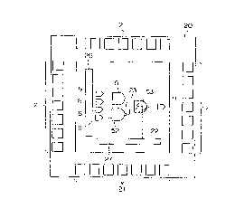
Figure 3 shows a semiconductor integrated circuit
device with fault detection function according to one
embodiment of the present invention. A semiconductor
integrated circuit
- 4b -
65259-144
2079696
device, generally designated by a reference numeral 20, includes
I/0 pads 21 respective ones of which are for components disposed
in the integrated circuit. The semiconductor integrated circuit
device 20 of the present invention includes logic function
blocks 51, 52, 53 etc. which are similar to the ones included
in the conventional integrated circuit device shown in Figure 1.
For the reason which will be described later, only the logic
function block 53, for example, is configured as a logic
function block with output signal potential sensing function
including a sense transistor 12 like the one shown in Figure
2. A sense line 22 and a probe line 23 are connected to the
logic function block 53. Input terminals 8 are connected to
a logic circuit formed by particular logic function blocks
for applying input signals thereto, and an output terminal
9 is connected to a logic circuit formed by another logic
function blocks for deriving an output signal therefrom. The
probe line 23 is connected to a probe line driver 26, and the
sense line 22 is connected to a signal reading sense line
receiver 27.
The semiconductor integrated circuit device with fault
detecting function of the present invention is designed and
fabricated based on the result of test, which is conducted
according to a flow chart such as one shown in Figure 4 to
determine as to whether fault conditions of particular logic
function blocks are detectable or not based on predetermined
input/output signal combinations.
In a step 101, a function testing input/output test pattern
is generated to perform a fault simulation for common semicon-
ductor integrated circuit devices.
Next, in a step 102, basic signals prepared according
to the input/output test pattern are used to find, if any,
the presence of fault-undetectable logic function blocks, i.e.
logic function blocks of which fault conditions cannot be
detected with such basic signals.
In a step 103, a logic function block with fault detecting
function including a sense transistor 12 like the one shown
2079696
in Figure 2 is substituted only for the fault-undetectable
logic function block found in the step 102 In the
semiconductor integrated circuit device of the present invention
shown in Figure 3, the logic function block 53 is the thus
substituted logic function block with output signal potential
sensing function.
By the above-mentioned technique, semiconductor integrated
circuit devices with a fault detecting capability increased
to 100% or to a desired level are fabricated. In a step 104,
the input/output signal combinations expected for ordinary
logic function blocks are used to detect if there is any fault
condition in any of ordinary logic function blOcksr and also
signals from logic function blocks with an output signal
potential sensing function are examined whether such blocks
are in fault condition or not. Thus, substantially all of
the logic function blocks in the semiconductor integrated
circuit device can be examined for fault conditions. Thus,
the semiconductor integrated circuit device which incorporates,
as part thereof, the logic function block 53 with output signal
potential sensing function for detecting a fault condition
thereof, shown in Figure 3, is provided.
In ordinary semiconductor integrated circuit devices,
30% to 40% of logic function blocks are ones of which fault
conditions cannot be detected by means of predetermined basic
signals prepared according to an input/output test pattern
as used in the step 102. Accordingly, in the semiconductor
integrated circuit device of the present invention, 30-40%
of the logic function blocks of the device are configured as
a logic function block with output signal potential sensing
function shown in Figure 2, and the rest, 60-70%, of the blocks
are tested based on predetermined input/output signal
combinations generated in response to a predetermined test
pattern.
In summary, according to the present invention, only those
logic function blocks of which fault conditions cannot be be
detected based on expected basic input/output signal
2079696
combinations produced in response to a predetermined test
pattern, are configured in a logic function block form so as
to have an output signal potential sensing function. This
can reduce the numbers of sense transistors, probe lines and
sense lines to 30-40% relative to the conventional semiconductor
integrated circuit device shown in Figure 1. In addition,
the sizes of a probe line driver and a sense line receiver
can be reduced. Thus, without reducing the fault detecting
capability, the areas of active region and wiring region which
are required for providing a fault detecting function can be
reduced, and, accordingly, the effective space usable for the
purpose of the integrated circuit function can be increased.