Note : Les descriptions sont présentées dans la langue officielle dans laquelle elles ont été soumises.
ASYMMETRICAL PULSE WIDTH MODULATED RESONANT DC/DC CONVERTER
Field of the Invention
The present invention relates generally to constant
5 frequency resonant DC/DC converters. In particular, it is directed to
pulse width modulated resonant DC/DC converters in which the output
voltage is controlled by ~e pulse width of sw;tching pulses while their
frequency stays constant. ;~
o Background of the Invention
In many advanced telecommunication systems, particulary
optical systems, Point of Use Power Supplies (PUPS) are used ~o supply
conditioned power to each electronic card. Some of the basic
requirements for this power conversion are:
(1~ High power density
~2) High efficiency
~3) Low EMI (both conducted and radiated), and
(4) Constant operating frequency
In order to achieve high power densities, there is a trend to
operate power supplies at higher switching frequencies. As the
switching frequencies increase, the switching losses associated with the
turn-on and turn-off of the devices in the power supplies also increase.
In switch mode power supplies, these losses are so significant that the
operation of the power supplies at very high frequencies are prohibitive
due to low conversion efficiencies. However~ in resonant mode power
supplies, the switching losses are low which allow the operation of
resonant converters at very high frequencies. The resonant mode
DC/DC converter can be classified into the following categories:
(1) Full-Resonant DCfDC converters
(2) Quasi-Resonant DC/DC converters
(3) Multi-Resonant DC/DC converters
~'
2 7
A number of U.S. Patents, e.g. Nos. 4~81as~962~ issued March
21,1989, to Magalhaes et al; 4,679,129, issued July 7,1989, to Sakakibara et
al; 4,355,243, i~sued October 19,1982, to Tellert; 4,935,857, issued June 19,
1990, to Nguyen et al; a~,992,91g, issued February 12,1991, to Lee et al; and
4,833,584, issued May 23,1989, to Divan, describe full-resonant DC/DC
converters. U.S. Patent Nos. 4,720,667 and 4,720,668, both issued to Lee et
~1 on January 19, 1988, on the other hand, disclose quasi-resonant DC: /VC
converters, while U.S. Patent Nos. 4,841,220, issued June 20, 1989, to
Tabisz et al, and 4,857,822, issued August 15,1989, to Tabisz et al teach
o multi-resonant I)C/DC converters. The converter topologies reported in
the referenced patents have reduced to near 2ero switching losses,
however, their output voltage is controlled and/or changed by varying
the operating/switching frequency. These converters are, therefore,
unsuitable for the application where system synchronization is required,
e.g. telecommunications.
The present inventor's co-pending U.S. patent applica-
tions, Serial Nos. 07/627,157 and 07/676,597, teach constant frequency
resonant DC/DC converters. These converters exhibit near zero
switching losses and can be operated at very high frequency. However,
their power and control circuitry are complex and have a high
component count. These converter circuits offer high power densities at
medium-to-high power levels, however, at low-to-medium power
levels, these converters do not give high power densities due to a high
component count.
Canadian Patent No. 1,167,916, issued May 22, 1984, to
White describes constant frequency half-bridge series resonant DC/DC
converters. This converter circuit uses symmetrical pulse-width
modulation {PWM.) to vary the periodic energization of the series tuned
circuit employed to drive a transformer and an associated rectifier. The
symmetrical PWM series resonant circuit as taught in the patent has the
following disadvantages:
.
.: .
. ~ .:
Q ~ 7
(1) turn-on and turn-off losses are present for both the
switches;
(2) high switching transient voltages are caused across
the switches due to recovery current of the body
diodes whenever the switeh is turned-off after the
conduction of its body diode.
(3) Any snubber capacitor (including drain-to-source
capacitor) which is placed across the switch to absorb
high switching transient voltages is discharged into
o the switch on turn-on. This gives rise to 1/2 CV2
losses.
The above losses increase with increasing switching
frequency. This limits the operation of the converter at high
frequencies.
Ob~ecb of the Invention
It is therefore an object of the present invention to provide
a constant frequency resonant DC/DC converter with improved
performance.
It is another object of the present invention to provide a
constant frequency resonant DC/DC converter which is able to operate at
a high switching frequency with high efficiency.
It is yet another object of the present invention to provide
a constant frequency resonant DC/DC converter in which the duty cycles
of t~e switching pulses are especially designed to give a higher efficiency.
Summary of the Invention
Briefly stated the present invention is directed to an
asymme~rical pulse width modulated constant frequency resonant
DC/DC converter. The converter comprises bridged chopper means for
converting a DC input to a constant high frequency AC and resonant
circuit means including a series resonant capacitor and a resonant
,
.
.. .. ... . . . ..
~0~7
inductor for sending the high frequency AC to high frequency
transformer means to generate a transformer secondary AC. It further
includes rectifier means connected to the high freqllency transformer
means to rectify the transformer secondary AC to produce a stable DC
output. The bridged chopper means include at least two seDniconductor
switches, each having a snubber capacitor connected thereacross. The
switches alternately conduct and the duty cycles of the conduction of the
switches are complementary with one another. The duty cycles are
further adjustable to maintain the stable DC output.
Brief Description of the Drawings
For a more complete understanding of the present
invention and for further objects and advantages thereof, reference may
now be made to the following description, taken in conjunction with
the accompanying drawings, in which:
Figure 1 is a circuit diagram of the resonant DC/DC
converter according to one embodiment of the present invention;
Figure 2 shows pulses applied to the switches and the
output voltage of the bridged chopper circuit;
Figure 3 is a fundamental equivalent circuit of the present
converter;
Figure 4 is a graph showing the output voltage against the
duty cycle;
Figure 5 illustrates wave forms of various parameters ln
time domain; and
Figures 6 and 7 depict circuit diagrams of converters
according to yet other embodiments of the present invention.
Detailed Description of the P~e~e~ed Embo~;limenti of the In~renLti~sn
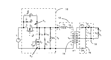
Figure 1 shows a circuit diagram of the Asymmetrical
Pulse Width Modulated ~APWM) series resonant DC/DC converter
according to one embodiment of the present invention. This circuit
2 ~
consists of a chopper circuit 10, a series resonant circuit 12, a high
frequency transformer 14, a rectifying circuit 16, and an output filter 18.
The chopper circuit 10 is a half bridge inverter and contains two switches
(Sl and S2), two diodes (Dl and D2) and two snubber capacitors (Cl and
5 ~2). Of course a full bridge inverter can be used in place of the half
bridge one with proper modifications. In this embodiment, high
frequency MOSFET switches (Ql and Q2) are employed for Sl and S2 and
while shown in the Figure, no external diode is required across the
switch as body diodes of the MQSFETs serve the function for Dl and D2-
10 The function of this chopper circuit is to convert DC input voltage tohigh frequency unidirectional voltage waveform Vs at its output.
The series resonant circuit 12 consists of a series capacitor
Cs and a series inductor Ls~ The function of capacitor Cs is twofold: ~a) it
blocks the DC component of output ~oltage Vs from passing to the high
15 frequency transformerj and (b) it forms a resonant drcuit together with
inductor Ls~ The function of the series resonant circuit is to convert the
unidirectional voltage Vs into resonating current iS. Although this
embodiment employs a series resonant circuit, other resonant circuits,
2.g. a parallel resonant circuit or a combination of both, can be used in its
20 placet as will be discussed later.
The high frequency transformer 14 provides matching and
isolation for the output voltage of the converter. The rectifying circuit
16 which includes diodes DR1 and DR2 converts the resonating current iS
into unidirectional current io at its output. The output filter 18 which
25 consists of a capacitor CO filters out the high frequency ripple current of
io and provides an essentially ripple free substantially constant output
voltage VO across the output load.
According to the present invention, the gating signals
applied to switches Sl and S2are such that they are complementary of
3 Q each other. This means that if duty cycle for switch S~ is D, then the duty
, - , ., ,. ~ -
- - . . . .
:;
2 ~
cycle for switch S2 should be (1-D). The asymmetrical PWM of the
converter produces an output voltage Vs as shown in Figure 2. The
time variation of Vs may be represented by the following Fourier series:
Vs = VjD ~ ~1.4V; / (n~)-(1-cos27mD)1/2-sin (nc~Ot+~n) (1)
5 where:
D = Duty cycle for switch S
n = order of nth harmonic
Vj = DC input voltage (V)
= fundamental switching frequency (r/s), and
0~n~ tan-l(sin?1rn~ cos2~cnD)) (2)
As explained earlier, the series capacitor Cs blocks the DC
component of voltage Vs~ Therefore, the AC component of Vs which
causes the resonant current to flow is given by:
VsaC = ~1.4Vj / (n~)-(1 cos27mD~l/2-sin(nc~ot+~n) (3)
15 In operation, each of the furldamental and harmonic
voltage components, given by equation (3), produces fundamental and
harmonic current through the series resonant circuit. However, to
explain the control of the output voltage of the converter, only a
fllnllanlental component is considered. Figure 3 shows the funda-
20 mental equivalent circuit of the converter. In the Figure, the inductive
and capacitive reactances are shown as well as resistive reactance of the
load.
The following relations are obtained from Figure 3 and
using equation (3):
25 Fundamental RMS voltage Vsl = V~ cos2~D)1/2 (4) ~
Fundamental RMS current IS1 - Vj / (ZS~ cos2~D)1/2 (5)
The average output current Io= O.9V; / (Zs~ (1 cos2~D)1/2 (6)
. ' ~
rl :
The output voltage of the converter VO = O.9VjRL / (Zs~ cos2~D~2 ~7)
= K(l-cos2~D)1~2 (8)
where:
RL = Resistive ou~kut load (Q)
Zsi~ Fundamental impedance at the input of resonant
circuit including output load (Q)
Figure 4 shows the output voltage of the converter as a
function of duty cycle D. This figure shows that ~he output voltage of
the converter can be varied, that is to say, controlled by changing the
o duty cycle D either from O to 0.5 (minimum-to-maximum output
voltage) or 0.5 to 1.0 (maximum-to-minimum output voltage~. ;
A description of the operation of the DC/DC converter as
shown in Figure 1 will now be given with reference to Figure 5 which
illustrates wave forms of various parameters in ~he time domain.
For a steady-state cycle, there exists four distinct intervals I,
II, III, and IV in which the converter operates. For each interval, the
operation of the converter is descrîbed below:
Interval I:
At the beginning of this interval gating signal Vgsl is
applied across the gate and source of switch Sl. Switch Sl starts to
conduct and the current flowing through anti-parallel diode Dl is now
carried by the switch. Since diode Dl was conducting prior to the
conduction of switch Sl, turn-on of the switch is, therefore, obtained
under zero voltage. This re~sults in zero turn-on losses. During this
interval a positive voltage Vi appears at the output of the chopper circuit
and power flows from the input DC source to the resonant circuit and
the output load.
Interval II:
At the ~egimling of this interval gating signal Vgsl from
the gate of switch Sl has been removed. Switch Sl starts to turn-off, and
the snubber capacitor Cl starts to charge. At the same time, because of
the positive resonant current iS~ the snuWer capacitor C2 across switch S2
starts to discharge to the resonant circuit. Once voltage across snubber
capacitor C2 reaches zero, the positive resonant current forces anti-
5 parallel diode D2 to conduct. A large value of snubber capacitor Cl isemployed across switch Sl to provide a slGw rise of voltage across switch
Sl, thereby eliminating turn-off loss in the switch. (It will be explained
during the description of Interval IV that the capacitor Cl discharges to
the resonant circuit, therefore, the snubber losses are zero.)
10 Interval III:
At the beginning of this interval gating signal VgS2 has
been applied across the gate and source of switch S2. The resonant
current flowing through anti-parallel diode D2 is now transferred to
switch S2. Since diode D2 was conducting prior ~o the conduction of
15 switch S2, turn-on of the switch is, therefore, obtained under zero
voltage which results in zero turn-on loss for the switch. During this
interval, the output voltage of the chopper is clamped to zero. No
additional energy from the DC source, during this interval flows to the
resonant circuit. However, the energy stored in the resonant
20 components during Interval I now free wheels through the switch S2
and keeps supplying power to ~e output load.
Interval IV:
At the beginning this interval gating signal VgS2 from the
gate of switch S2 has been removed. Switch S2 starts to turn-off and
25 snubber capacitor C2 starts to charge. At the same time because of the
negative resonant current iS, the snubber capacitor Cl starts to discharge
to the resonant circuit. Once the voltage across capacitor Cl reaches zero,
the negative resonant current forces anti-parallel diode Dl to conduct.
Since the capacitor Cl discharges to the resonant circuits, the snubber
30 losses are essentially zero. As explained in Interval II, snubber capacitor
.. ... .. .
- . ~ .. ,... , ~ ~ . .
2~f~27
C2 also discharges to the resonant circuit and therefore permits the use
of a large capacitance across switch S2. Ihis provides a slow rise of
voltage across switch S2 which eliminates turn-off losses of the switch.
The above description of the converter operation reveals
that the switches are always turned-on and turned-off Imder zero
voltage, thereby eliminating the switching losses. Furthermore, the
snubber capacitors always discharge to t~e resonant circuit, which also
eliminates the snubber losses.
The APWM resonant converter (Asymmetrical PWM
o converter according to the present invention) and a PWM resonant
converter (symmetrlcal PWM converter of prior art) were compared for
their performance. The table appended at the end of the disclosure
shows the efficiencies for these two converters as a function of input
voltage at 1 MHz operating frequency. As can be seen from this table,
the efficiency of the APWM converter is about 15~ higher than the
efficiency of the PWM converter circuit at a nominal voltage of 60V.
Figure 6 shows an APWM parallel resonant DC/DC con-
verter according to another embodiment of the present invention. The
configuration of this circuit is essentially the same as that of the
conYerter circuit of Pigure 1 except that the resonant inductor Lpis
placed in parallel with the output transformer. This configuration has
the advarltage that the parallel inductor can easily be integrated with the
transfor~er which results in a reduced count of power components.
Figure 7 shows one other embodiment of the APWM
resonant converter. This circuit has a similar configuration as the circuit
of Figure 6 except that an additional capacitor Cp is placed across the
inductor and the output filter has one inductor and one capacitor.
Although this configuration has a higher power component count, it is
better s1i~ted for applications wi~ ultra low ripples in output voltage.
The new class of Asymmetrical Pulse Width Modulated
Resonant Converter Topology of the present invention has simple
. ' ~ .. '' ~ ' '
. .
power and control circuitry, and exhibits near zero switching losses at
constant operating frequency. Initial bread-board results show
significant potential of their use in all future applications where a
distributed power architecture is chosen to power high speed digital
5 CiICUitS in a system.
INPUT EFFICIENCY E~FICIENCY
VOLTAGE RROPOSED ART PRIOR ART
50V 88.5% ~7.0%
50V 88.3% 80.0%
60V 88.2% 73.0~
65V 88.5% 70.0%
7~V ~7.0% 65.0%
75V 84.5% 62.0%
T~BLE: COMPARISON OF EFFICIENCIES
Operatlng 3Frequency = 1 MHz
Output Voltages = 5 V ~ 3 A
= 15 V ~ lA
~, ,