Sélection de la langue

Search

Sommaire du brevet 2080450 

Énoncé de désistement de responsabilité concernant l'information provenant de tiers

Une partie des informations de ce site Web a été fournie par des sources externes. Le gouvernement du Canada n'assume aucune responsabilité concernant la précision, l'actualité ou la fiabilité des informations fournies par les sources externes. Les utilisateurs qui désirent employer cette information devraient consulter directement la source des informations. Le contenu fourni par les sources externes n'est pas assujetti aux exigences sur les langues officielles, la protection des renseignements personnels et l'accessibilité.

Disponibilité de l'Abrégé et des Revendications

L'apparition de différences dans le texte et l'image des Revendications et de l'Abrégé dépend du moment auquel le document est publié. Les textes des Revendications et de l'Abrégé sont affichés :

  • lorsque la demande peut être examinée par le public;
  • lorsque le brevet est émis (délivrance).
(12) Brevet: (11) CA 2080450
(54) Titre français: CIRCUIT DE COMMANDE DE SALVES POUR SYSTEME DE COMMUNICATION AMRT
(54) Titre anglais: BURST CONTROL CIRCUIT FOR USE IN TDMA COMMUNICATIONS SYSTEM
Statut: Périmé et au-delà du délai pour l’annulation
Données bibliographiques
(51) Classification internationale des brevets (CIB):
  • H04B 01/04 (2006.01)
  • H03G 03/20 (2006.01)
  • H04B 07/212 (2006.01)
(72) Inventeurs :
  • HASHIMOTO, KAZUYA (Japon)
  • HORIKOSHI, DAIJI (Japon)
(73) Titulaires :
  • NEC CORPORATION
(71) Demandeurs :
  • NEC CORPORATION (Japon)
(74) Agent: G. RONALD BELL & ASSOCIATES
(74) Co-agent:
(45) Délivré: 1998-08-11
(22) Date de dépôt: 1992-10-13
(41) Mise à la disponibilité du public: 1993-04-15
Requête d'examen: 1992-10-13
Licence disponible: S.O.
Cédé au domaine public: S.O.
(25) Langue des documents déposés: Anglais

Traité de coopération en matière de brevets (PCT): Non

(30) Données de priorité de la demande:
Numéro de la demande Pays / territoire Date
293736/1991 (Japon) 1991-10-14

Abrégés

Abrégé français

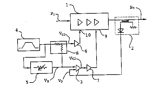
L'invention est un circuit de contrôle de salves pour système de communication AMRT qui comprend un amplificateur de puissance ayant deux bornes de contrôle distinctes. Un signal de contrôle de niveau, qui est constitué de la différence entre un signal de référence et le niveau du signal de salve de sortie de l'amplificateur, contrôle par rétroaction le niveau du signal de salve de sortie par l'intermédiaire de la première borne de contrôle, et un signal de contrôle de forme d'onde ayant une forme d'onde prédéterminée contrôle la forme d'onde du signal de salve de sortie par l'intermédiaire de la seconde borne de contrôle. Quand le niveau du signal de référence baisse, l'amplitude du signal de contrôle de forme d'onde baisse en fonction de ce niveau.


Abrégé anglais


A burst control circuit for use in a TDMA communications system
comprises a power amplifier having two separate control terminals.
A level control signal which is the difference between a reference
signal and the level of the output burst signal of the amplifier,
feedback-controls the level of the output burst signal through
first control terminal, and a waveform control signal having
predetermined waveform, controls the waveform of the output burst
signal through a second control terminal. When the level of the
reference signal is decreased, the amplitude of the waveform
control signal is decreased as a function of the level of the
reference signal.

Revendications

Note : Les revendications sont présentées dans la langue officielle dans laquelle elles ont été soumises.


-7-
We claim:
1. A burst control circuit for use in a TDMA communications system
comprising:
power amplifier means having first and second control terminals
for amplifying an input radio signal to produce an output burst
signal, said amplifier means changing the level and waveform of
said output burst signal in response to level and waveform control
signals which are supplied through said first and second control
terminals, respectively;
ALC circuit means for generating a level control signal on the
basis of a signal representing a difference between the level of a
reference signal and the level of said output burst signal, and
supplying the generated level control signal to said first control
terminal as said level control signal; and
waveform control circuit means for generating a waveform control
signal having a predetermined waveform and an amplitude which is a
function of the amplitude of said reference signal, and supplying
the generated waveform control signal to said second control
terminal as said waveform control signal.
2. A burst control circuit as claimed in claim 1, wherein said
reference voltage is obtained from a trapezoidal wave generator
through a variable attenuator, said trapezoidal wave generator
generating a signal having said predetermined waveform.
3. A burst control circuit as claimed in claim 2, wherein said
waveform control signal is synthesized by a voltage synthesizer
from said reference signal and the output signal of said
trapezoidal wave generator.

-8-
4. A burst control circuit as claimed in claim 1, wherein the level
of said output burst signal is detected by a detector which detects
the output of a directional coupler coupled to said output burst
signal.
5. A burst control circuit as claimed in claim 4, wherein said
level control signal is produced by a differential amplifier which
amplifies the difference between said reference signal and the
output of said detector.
6. A method of controlling a burst signal, comprising the steps of:
generating a level control signal on the basis of a signal
representing a difference between the level of a reference signal
and the level of an output burst signal;
generating a waveform control signal having a predetermined
waveform and an amplitude which is a function of the amplitude of
said reference signal; and
amplifying an input radio signal to produce said output burst
signal in accordance with said level and waveform control signals.
7. A method as claimed is claim 6, wherein said step of generating
a waveform control signal comprises the steps of:
generating an original signal having gently sloped leading and
trailing edges;
attenuating the amplitude of said original signal to produce
attenuated signal as said reference signal; and
attenuated said original signal and said attenuated signal to
produce a combined signal as said waveform control signal.

Description

Note : Les descriptions sont présentées dans la langue officielle dans laquelle elles ont été soumises.


FP.GM I.P. ~IV1~10N NEC 1'~ ~10~12~(~) 13.19 ~3=-~,31102ll9~40 P. 3
2080'450
-
~URST CONTROL C~RCUIT FOR USE r~ TD~A COK~NI~ATION~ SYSTE~
BACKGROUND OF THE INVENTION
This in~ention relates to a bu~st control circuit fo~ use in
time division ~ultiple access(TDMA) co~ nication~ system.
One of the prior arts of this inven~ion is disclosed in U.S.
P~tent No.5,lOl,176entitled~BURST CONTROL CIRCU~T FOR USE IN TD~A
CONMUNICATIONS SYSTEM~ ~hich is assigned to the same assignee as
the present application. ~nd whieh will hereafter be called the
prior circuit.
In the prior circuit, a power amplifier having two cont~ol
terminals amplifies an input radio signal to produce an output
bu~st signal. A level control signal representin~ a difference
between a reference si~n~l ~nd the level of the output burst signal,
feedback-cont~ols the level of the output bu~st si~nal thro~h a
first control terminal of the a~plifier. A waveform control signal
of a fixed amplitude controls the wavefo~m of the output burst
signal throtlgh a second control te~minal of the amplifier.
The ~aveform control si~nal has a trapezoid~l w~veform and the
~O xise and fall times of the waveform cont~l signal are so determined
that the spectrum bandwid~h of the output burst si~n~l is
suppressed within ~n allowable range.
A non-linear po~er a~plifier havin~ ~ hi~h power eff~ciency is
used as the power ~mplifier of the prior circuit. In ~ small powe~
2~ output ran~e of this non-linear powe~ amplifier. ~ sm~ll in~rement
of the level control signal causes an e~cessively large increment
of the output burs~ si~nal.

F~O~ i.P. DIYI~IGi~ N~C l'~J~2~10~12~(~) 13:20 ~ 311021)9040 P. 4
2080450
This characteristic of the power amplifier makes i~ difficult to
carry out ~ ~ine level control in a small powe~ outPut range. And
this e.Ycessively hi~h ~ain of the a~plifier in a small powe~ r~nge
o~tendete~ioratesthestabilityof thefeedback-control, ~esulting
in overshoots in the le~in~ ~nd tr~iling edges of the waveform.
BRIEF DESCRIPTION OF THE INVENTION
Therefo~e, a primar~ object of the present invention is to p~ovide
a burst cont~ol circ~it which can control a same a~pli~ier as used
in the prior circuit, with ~ required p~ecision and ~ suffi~ient
stability fo~ ~11 the r~nges of the output.
For this obiect, the ~mplitude of the waveform control signal is
chan~ed as a function of the amplitud~ of the ~eference signal.
~ hen ~ ~ontrolled output of the power amplifie~ is small, the
amplitude of the reference signal is set at a low level, and the
amplitude of the waveform control signal becomes s~a~1, The small
a~plitude of the ~aveform control ~ignal suppresses the gain of t~e
power amplifier in ~ small power output range and makes the control
by the level control ~ignal easier.
Acco~ding to the present invention,there is provided a burst
control circuit for use in a T~A ~ommunication~ ~ystem.
comprising: power amplifier means having first and second control
terminals fo~ amplifying an input radio signal to produce an output
burst signal, the amplifier means ~h~n~ing the level and wa~eform
of the output burst signal in response to level and waveform control
signals which are suPPlied thro~gh ~he first and the second control
terminals, respectivel~: ALC(automatic level control) circuit
means ~o~ generatin~ ~ level cont~ol si~nal on the basis of a sign~1

n~.OM l P. DIViSlON. ~EC l~ l29(~) 13:20 ~ 3l~ ?o~o P, 5
2080450
_ 3-
representin~ a difference between a reference signal and the level
of the output burst si~nal, and supplying the gener~ted level
control signal to the first control ter~inal as the level control
sign~l; and wa~eform control circuit means for generating a
~avefon~ control signal having a predetermined ~veform and an
amplitude w~ich is a function of the amplitude of the referen¢e
si~nal. and s~pplying the generated ~eform control signal to the
second control terminal as the waveform control si~nal.
BRIE~ ~ESCRIPTION OF THE ~A~INGS
Further objects, fe~tures, and advantages of this invention will
b~co~e apPa~ent from a consideration of the following description,
the appended clai~s, and the a~companyin~ drawings.
Fig.1 is a block dia~ra~ illustratin~ an embodi~ent of the present
invention.
Fig.2 shows an input to output char~cte~istic of an embodiment
shown in ~
~ETA~LED ~ESC~IPTION O~ THE PREFERRE~ E~BOD~ENTS
In Fig.l. a power amplifier 1. haYlng a high po~er effic~ency,
amplifies an input radio signal ~Ito produce an outp~t burst signal
PO. A detector 2 including a directional coupler detects the output
~urs~ si~nal PO and p~oduces a voltag~ VD representing the level of
the output burst signal PO.
A trapezoidal wave ~enerator4 generates ~ trapezoidal wave sign~l
for modul~ting the waYeform o~ the output burst signal PO. The
trapezoidal wave signal h~s ~ently slopped le~ing and trailin~
edges. The input radio si~nal Pl ~ay be a continuou~ signal or a
burst signal, and ~hen Pl is a bu~st signal. the trapezoidal wave

~ O ~ ~ 4 5 o
signal vc1 must be synchronized with the input burst signal.
The output vc1 of the trapezoidal wave generator 4 is attenuated by a variable
attenuator 5 to produce a variable reference signal VR. A differential amplifier
3 produces an error signal Vc2 which is proportional to (VR_VD). The error signal
5 or the level control signal Vc2 feedback-controls the level of the output burst
signal P0 through another current booster 7 and a first control terminal 9 of the
power amplifier 1. Thus, the power amplifier 1, the detector 2, the differential
amplifier 3, the current booster 7, and the control terminal 9 constitute an ALC
circuit. The circuit elements, except for elements 5, 6 and 8, are explained in
detail in the above-mentioned U.S. Patent No. 5,101,175.
A voltage synthesizer 8 produces a waveform control signal Vc3 having an
amplitude which is a function of the amplitude of the reference signal VR.
The waveform control signal Vc3 modulates the amplitude of P0 through a
current booster 6 and a second control terminal 10 of the power amplifier 1.
15 The attenuator 5 and voltage synthesizer 8 are the feature elements of the
present invention and play very important roles as described in detail below.
Refer,i"y also to Fig. 2, a solid line illusl~ates an input to output characteristic
of the prior circuit, and a chain line illusl,dtes an input to output characteristic of
the circuit shown in Fig. 1.
20 For the sake of comparison, the solid line in Fig. 2 is explained
B

F~OM l.F. DIVISION. NEC 1'~$10~12~(~) 13:21 ~ 311q2~ 040 P. 7
~5~ 2080450
-
in the first pla~e. The block ~iagram of the p~ior circuit will be
represented by ~ig.l. ~hen the voltage synthesi2e~ 8 is eliminated
and the trapezoidal ~ave signal Vcl of a fixed amplitude is directly
connected to the input of the eurrent booster 6. Th~s the le~el
S control o~ the prior circ~it depends entirely on the e~ro~ signal
c2
The open loop ~haracteristi~ o~ Vc2 to PO (PO i~ me~sured by dB
~¢ale) of the power amplifier 1 is as shown by the solid line in
Fig.2.
As dPo/d~C2 is very large in ~ ~all power range, a ~ine contro1 o~
the output powe~ PO is ~ery difficult in this ran~e.
~ eturning to Fig.l. and assuming that the attenuator 5 is ~et at
a point whe~e V~=nYc~ ), that the resistance between Vcl ~nd V~
is R. and that the resistance between VR and Yc3 is mp we obt~in
(Vc3/Vcl~=(ntm)/(ltm)=A~ 2)~ This value of A is an ext~
attenuation caused by ~sing the waveform control si~nal Vc3 instead
of vcl~
a=2010gA~(3) represents the extra attenuation in dB scale. In
Fig.2, when Vczz8~ corresponds to n=1, VC2-4V corresponds to n-0.5.
We can select an appropriate value for m and c~lc~l~te the values
of a for the values o~ Vc2 b~7 equations (2) ~nd (3). Subt~acting
these values of ~ from the solid line in ~ t corresponding
points of Vc~, we obtain the chain line in ~ig.~.
Therefo~e, the chain line in Fig.~ illustrates the control
cha~cter~stic of vcg when there is the extra attenuation a.
It is appa~ent th~t the cont~l characteristic of the chain line
is substantially i~proved in a low power range compared wit~

F.-;Ol.,lI.P. DIVISION. NEC 1'''~ 10~12~(~) 13.22 ~a~ l IC~ O lO P~ ~
-6- 2080'~50
that of the solid line. As 2 result, the burst control ci~cuit
acco~ing to the present invention has a substantiall~ equal, and
a considerably high resol~tion o~er all the ran~es of the output
po~er PO. Thus it is easy to finely control the output power PO oYe~
all the ran~es of ~ame.
In the embodi~ent sh~wn in ~ig.l, the waveform control signal Yc9
is synthesi~ed by the voltage s~nthesize~ $. ~t must be noted,
howeve~.~hat there a~e many different means for ~enerating a
~aveform control signal havin~ an ~mplitude ~hich is ~ function of
the amplitude of the reference signal, and that any of these means
is applicable to this invention.

Dessin représentatif
Une figure unique qui représente un dessin illustrant l'invention.
États administratifs

2024-08-01 : Dans le cadre de la transition vers les Brevets de nouvelle génération (BNG), la base de données sur les brevets canadiens (BDBC) contient désormais un Historique d'événement plus détaillé, qui reproduit le Journal des événements de notre nouvelle solution interne.

Veuillez noter que les événements débutant par « Inactive : » se réfèrent à des événements qui ne sont plus utilisés dans notre nouvelle solution interne.

Pour une meilleure compréhension de l'état de la demande ou brevet qui figure sur cette page, la rubrique Mise en garde , et les descriptions de Brevet , Historique d'événement , Taxes périodiques et Historique des paiements devraient être consultées.

Historique d'événement

Description Date
Inactive : CIB de MCD 2006-03-11
Le délai pour l'annulation est expiré 2002-10-15
Lettre envoyée 2001-10-15
Accordé par délivrance 1998-08-11
Préoctroi 1998-04-16
Inactive : Taxe finale reçue 1998-04-16
Inactive : Correspondance - Poursuite 1997-10-29
Un avis d'acceptation est envoyé 1997-10-24
Lettre envoyée 1997-10-24
Inactive : Renseign. sur l'état - Complets dès date d'ent. journ. 1997-10-20
Inactive : Dem. traitée sur TS dès date d'ent. journal 1997-10-20
Inactive : CIB enlevée 1997-09-25
Inactive : CIB en 1re position 1997-09-25
Inactive : CIB attribuée 1997-09-25
Inactive : Approuvée aux fins d'acceptation (AFA) 1997-09-22
Demande publiée (accessible au public) 1993-04-15
Exigences pour une requête d'examen - jugée conforme 1992-10-13
Toutes les exigences pour l'examen - jugée conforme 1992-10-13

Historique d'abandonnement

Il n'y a pas d'historique d'abandonnement

Taxes périodiques

Le dernier paiement a été reçu le 1997-10-03

Avis : Si le paiement en totalité n'a pas été reçu au plus tard à la date indiquée, une taxe supplémentaire peut être imposée, soit une des taxes suivantes :

  • taxe de rétablissement ;
  • taxe pour paiement en souffrance ; ou
  • taxe additionnelle pour le renversement d'une péremption réputée.

Les taxes sur les brevets sont ajustées au 1er janvier de chaque année. Les montants ci-dessus sont les montants actuels s'ils sont reçus au plus tard le 31 décembre de l'année en cours.
Veuillez vous référer à la page web des taxes sur les brevets de l'OPIC pour voir tous les montants actuels des taxes.

Historique des taxes

Type de taxes Anniversaire Échéance Date payée
TM (demande, 5e anniv.) - générale 05 1997-10-14 1997-10-03
Taxe finale - générale 1998-04-16
TM (brevet, 6e anniv.) - générale 1998-10-13 1998-10-05
TM (brevet, 7e anniv.) - générale 1999-10-13 1999-09-17
TM (brevet, 8e anniv.) - générale 2000-10-13 2000-09-25
Titulaires au dossier

Les titulaires actuels et antérieures au dossier sont affichés en ordre alphabétique.

Titulaires actuels au dossier
NEC CORPORATION
Titulaires antérieures au dossier
DAIJI HORIKOSHI
KAZUYA HASHIMOTO
Les propriétaires antérieurs qui ne figurent pas dans la liste des « Propriétaires au dossier » apparaîtront dans d'autres documents au dossier.
Documents

Pour visionner les fichiers sélectionnés, entrer le code reCAPTCHA :


Pour visualiser une image, cliquer sur un lien dans la colonne description du document (Temporairement non-disponible). Pour télécharger l'image (les images), cliquer l'une ou plusieurs cases à cocher dans la première colonne et ensuite cliquer sur le bouton "Télécharger sélection en format PDF (archive Zip)" ou le bouton "Télécharger sélection (en un fichier PDF fusionné)".

Liste des documents de brevet publiés et non publiés sur la BDBC .

Si vous avez des difficultés à accéder au contenu, veuillez communiquer avec le Centre de services à la clientèle au 1-866-997-1936, ou envoyer un courriel au Centre de service à la clientèle de l'OPIC.

({010=Tous les documents, 020=Au moment du dépôt, 030=Au moment de la mise à la disponibilité du public, 040=À la délivrance, 050=Examen, 060=Correspondance reçue, 070=Divers, 080=Correspondance envoyée, 090=Paiement})


Description du
Document 
Date
(aaaa-mm-jj) 
Nombre de pages   Taille de l'image (Ko) 
Dessins 1997-08-20 2 16
Description 1997-08-20 6 232
Description 1994-01-28 6 235
Revendications 1994-01-28 2 82
Abrégé 1994-01-28 1 21
Dessins 1994-01-28 2 37
Dessin représentatif 1998-10-25 1 7
Dessin représentatif 1998-07-27 1 6
Avis du commissaire - Demande jugée acceptable 1997-10-23 1 165
Avis concernant la taxe de maintien 2001-11-12 1 178
Taxes 1998-10-04 1 43
Correspondance 1998-04-15 1 40
Taxes 1997-10-02 1 44
Taxes 1999-09-16 1 42
Taxes 2000-09-24 1 45
Taxes 1996-10-03 1 53
Taxes 1994-10-11 1 35
Taxes 1995-10-11 1 32
Demande de l'examinateur 1996-02-21 1 56
Courtoisie - Lettre du bureau 1993-03-18 1 19
Courtoisie - Lettre du bureau 1993-05-18 1 52
Correspondance de la poursuite 1996-06-25 2 46
Correspondance de la poursuite 1996-04-29 1 25