Note : Les descriptions sont présentées dans la langue officielle dans laquelle elles ont été soumises.
2080563
- 1 -
TITLE OF THE INVENTION
TOTAL INTERNAL REFLECTION-TYPE
OPTICAL ~VAVEGUIDE SWITCH
BACKGROUND OF THE INVENTION
Field of the Invention
The present invention relates to a total internal
reflection-type optical waveguide switch, and more
particularly, to a total internal reflection-type
optical waveguide switch lowered in the level of
initial crosstalk at the time of switching operation.
Description of the Prior Art
In the field of optical communication, a total
internal reflection-type optical switch is used for
optical path switching. A semiconductor-type optical
waveguide switch, as an example of this total internal
reflection-type optical switch, will now be described
with reference to the accompanying drawings.
Fig. 1 is a schematic plan view showing a
conventional example of the total internal
reflection-type optical waveguide switch. In Fig. 1,
two optical waveguides 1 and 2 cross at an angle B ,
thus forming a crossing section 3. If light is
incident as indicated by arrow p, optical waveguides
la and 2a both function as incidence-side optical
waveguides, while optical waveguides lb and 2b both
function as emission-side optical waveguides. A
refractive index changing region 4 is formed at the
crossing section 3 between the optical waveguides.
The portion of each optical waveguide other than
the refractive index changing region 4 is constructed
in the manner shown in the sectional view of Fig. 2,
- 2 - 208 05 fi 3
which is taken along line II-II of Fig. 1. If GaAs
and AlGaAs are used as semiconductor materials, for
example, a substrate 12 of GaAs is formed on the back
of a lower electrode 11, and n'GaAs is built up to
form a buffer layer 13 on the substrate 12.
A lower cladding layer 14 of n'AlGaAs and a core
layer 15 of n-GaAs are successively formed on the
buffer layer 13. Then, an upper cladding layer 16 of
n-AlGaAs and a cap layer 17 of n-GaAs are successively
formed on the core layer 15, and are etched to form a
ridge-shaped optical waveguide. The whole resulting
structure is covered by an insulating film 18 of Si02
or the like.
As shown in the sectional view of Fig. 3, which
is taken along line III-III of Fig. 1, on the other
hand, a diffused region 4a is formed in the refractive
index changing region 4 by diffusing a predetermined
amount of an impurity, such as Zn, into the upper
cladding layer 16 so that the impurity nearly reaches
the core layer 15. A slit-shaped insulating film
aperture 18a is formed by partially removing the
insulating film 18, which covers the surface of the
crossing section 3, for a predetermined width with
respect to the longitudinal direction of the crossing
section 3. Then, an upper electrode 19 is mounted on
the insulating film aperture 18a.
In the case of this optical waveguide switch, if
light is applied to the incidence-side optical
waveguide 2a, as indicated by arrow p in Fig. 1,
without causing any operation between the upper and
lower electrodes 19 and 11, the light directly
advances straight through the crossing section 3, and
- 2080563
- 3 -
emerges from the emission-side optical waveguide 2b,
as indicated by arrow ~.
If electric current of a predetermined value, for
example, is injected from the upper electrode 19 via
the insulating film aperture 18a, however, the
refractive index of that portion of the core layer 15
which is situated under the refractive index changing
region 4 is lowered. As a result, a boundary surface
4b between the refractive index changing region 4,
whose refractive index is lowered, and the optical
waveguides, whose refractive index is not lowered,
develops at the crossing section 3. The boundary
surface 4b is situated on a straight line which
bisects the intersection angle 8 .
Accordingly, the incident light upon the
incidence-side optical waveguide 2a changes its
optical path toward the emission-side optical
waveguide lb, with the boundary surface 4b used as a
reflective surface, as indicated by broken line q' in
Fig. l, and then emerges from the waveguide lb. Thus,
the boundary surface 4b of the refractive index
changing region 4 is made to be a totally reflective
surface by the current injection, and the light is
totally reflected by this surface, so that a switching
function develops.
In the case of the optical waveguide switch
described above, however, the insulating film aperture
has the form of a slit, so that the boundary surface
4b of the refractive index changing region 4, which is
formed by diffusing Zn through the insulating film
aperture, has a flat configuration.
At the crossing section 3, the refractive index
2080563
- 4 -
changing region 4 contains different materials, so
that the refractive index of the remaining portions of
the optical waveguides is finely different from that
of the region 4. Even when no electric current is
injected from the electrode 19, therefore, the light
incident upon the incidence-side optical waveguide 2a
is reflected or refracted by the boundary surface 4b,
resulting in an optical loss. Thus, the initial
crosstalk level in the through state is high.
OBJECT AND SUMMARY OF THE INVENTION
The object of the present invention is to provide
a total internal reflection-type optical waveguide
switch capable of reducing the optical loss at the
time of switching operation, thereby lowering the
initial crosstalk level.
In order to achieve the above object, according
to the present invention, there is provided a total
internal reflection-type optical waveguide switch
which comprises optical waveguides crossing each other
so that a refractive index changing region for
reflecting light is formed at a crossing section
between the waveguides, the refractive index changing
region having a concave reflective surface recessed
with respect to one lateral portion of the crossing
section.
At the crossing section of the total internal
reflection-type optical waveguide switch according to
the present invention, the boundary surface
(reflective surface) based on a refractive index
difference caused by the difference in material
between the refractive index changing region and the
2080563
- 5 -
remaining portions of the optical waveguides is concave.
When the refractive index changing region is not
activated, therefore, light propagated from an incidence-side
optical waveguide to the boundary surface is less sensitive to
changes of the refractive index in the refractive index
changing region than in the case where the boundary surface is
flat, so that the initial crosstalk level can be lowered.
In accordance with the present invention there is
provided a total internal reflection-type optical waveguide
switch, made of semiconductor material, the optical waveguide
switch comprising: a pair of semiconductor optical waveguides
crossing each other so that a refractive index changing region
for reflecting light is formed at a crossing section between
the waveguides of said pair of optical waveguides; said pair
of optical waveguides and said refractive index changing
region all being made of laminated layers of a semiconductor
material, respectively; an electrode on said ref ractive index
changing region for applying electrical energy to said
refractive index changing region; and said refractive index
changing region having a smoothly curved concave reflective
surface recessed with respect to a lateral portion of said
crossing section.
BRIEF DESCRIPTION OF THE DRAWINGS
Fig. 1 is a schematic plan view showing a
conventional total internal reflection-type optical waveguide
swit ch;
72465-48
208 05 6 3
- 5a -
Fig. 2 is a sectional view taken along line II-II of
Fig. 1;
Fig. 3 is a sectional view taken along line III-III
of Fig. 1;
Fig. 4 is a schematic plan view showing an
embodiment of an optical switch acCOrding to the present
invention;
Fig. 5 is a graph showing the switching
characteristics of the optical switch of Fig. 4;
Fig. 6 is a graph showing the switching
characteristics of a modification of the optical switch of
Fig. 4;
Fig. 7 is a graph showing the switching
characteristics of another modification of the optical switch;
Fig. 8 is a schematic plan view showing another
embodiment of the optical switch according to the invention.
72465-48
2080563
-6-
Fig. 9 is a graph showing the switching
characteristics of the optical switch of Fig. 8;
Fig. 10 is a graph showing the switching
characteristics of a modification of the optical
switch of Fig. 8; and
Fig. 11 is a schematic plan view showing still
another embodiment of the optical switch according to
the invention.
DETAILED DESCRIPTION OF TAE PREFERRED EI~BODII~NTS
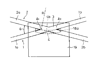
Fig. 4 is a plan view showing an example of a
switch according to the present invention.
The general construction of this switch differs
from that of the total internal reflection-type
optical waveguide switch of the conventional
construction shown in Fig. 1 only in the configuration
of the boundary surface between the refractive index
changing region 4 and the remaining portions of the
optical waveguides at the crossing section.
More specifically, the boundary surface of the
refractive index changing region 4 is shaped so that
the portion thereof extending from an intersection A1
between incidence-side optical waveguides la and 2a to
an intersection A2 between emission-side optical
waveguides lb and 2b has a concave which is recessed
with respect to that lateral portion of the crossing
section 3 on the side of the incidence-side optical
waveguide 2a (and emission-side optical waveguide lb),
as shown in Fig. 4.
In this case, the concave may, for example, be a
curved surface defined by a circular arc having a
fixed curvature radius R or a curved surface defined
2080563
_ 7 _
by a curve with a gradually varying curvature radius,
such as the circumference of an ellipse.
The following is a definite description of an
example of a method for manufacturing this optical
switch.
As shown in Figs. 2 and 3, for example, the
buffer layer 13 of e.g. n'GaAs, lower cladding layer
14 of e.g. n'AlGaAs, core layer 15 of e.g. n-GaAs,
upper cladding layer 16 of e.g. n-AlGaAs, and cap
layer 17 of e.g. n-GaAs are successively built up on
the substrate 12 of n'GaAs by the MOCVD process.
Then, the other portion of the surface except the
insulating layer aperture 18a of Fig. 4 is covered
with a masking material, and Zn is diffused through
the aperture 18a to form the Zn-diffused region 4a
which reaches the upper surface of the core layer 15.
The configuration of the diffused region 4a includes
the curved surface which is curved between the
intersections A1 and A2 of Fig. 4 and defined by the
circular arc having the curvature radius R.
Thereafter, the masking material is removed, the
cap layer 17 and the upper cladding layer 16 are
etched so that the light to be guided is in a single
mode, and the incidence-side optical waveguides la and
2a, the emission-side optical waveguides lb and 2b,
and the crossing section 3 are formed each in the
shape of a ridge so that the intersection angle is 8 .
Subsequently, the insulating film 18 of e.g. Si02
is formed on the whole surface of the resulting
structure, the portion corresponding to the insulating
film aperture 18a shown in Fig. 1 is removed by
etching, and the upper electrode 19 of, e.g. Ti/Pt/Au,
Zo8o5s3
_8_
is mounted there. Finally, the lower surface of the
GaAs substrate 12 is polished, and the lower electrode
11 of, e.g. AuGeNi/Au, is mounted thereon.
Although the semiconductors have been described
as the materials of the switch, the present invention
is not limited to this, and the switch may
alternatively be formed of a dielectric material, such
as LiNb03. If the material composition of the
refractive index changing region is changed, moreover,
switching operation can be performed by applying
voltage from the upper electrode.
Embodiment 1
The buffer layer 13 of n'GaAs 0.5 a m in
thickness, lower cladding layer 14 of n~Alo.2Gao.8As
3.0 a m in thickness, core layer 15 of n-GaAs 0.8 a m
in thickness, upper cladding layer 16 of n-
Alo.ZGao.BAs 0.8 a m in thickness, and cap layer 17 of
n-GaAs 0.2 a m in thickness were successively built up
on the n'GaAs substrate 12 by the MOCVD process. By
doing this, an optical switch, such as the one shown
in Fig. 4, was manufactured having the curvature
radius R of 5 mm and the intersection angle B of 4° .
Fig. 5 shows the switching characteristics of
this optical waveguide switch for the light of 1.55
a m wavelength.
In Fig. 5, a circle represents the emission power
from the emission-side optical waveguide 2b obtained
when the light is applied from the incidence-side
optical waveguide 2a, and a black spot represents the
emission power from the emission-side optical
waveguide lb.
When no electric current is injected from the
208 05 6 3
- 9 -
upper electrode 19, as seen from Fig. 5, the incident
light advances straight through the crossing section
3, and propagates toward the emission-side optical
waveguide 2b. As the injected current increases, the
emission power from the emission-side optical
waveguide lb increases, thus enabling switching
operation at about 200 mA.
As seen from Fig. 5, moreover, the initial
crosstalk level of this optical switch is about 18.5
dB. As compared with about 9.2 dB for the initial
crosstalk level of the optical switch with the
construction of Fig. 1 in which the reflective surface
of the refractive index changing region is flat, this
value indicates that the optical loss of the resulting
optical switch is very small.
Embodiment 2
An optical waveguide switch was manufactured in
the same manner as Embodiment 1 except that the
semiconductor compositions for the lower and upper
cladding layers 14 and 16 were n'Alo.~Gao_9As and n-
Alo.~Gao_9As, respectively, core layer 15 of n-GaAs
was 1.0 a m in thickness, and that the intersection
angle 8 was 5° .
Fig. 6 shows the switching characteristics of
this optical waveguide switch for the light of 1.55
a m wavelength.
In Fig. 6, a circle represents the emission power
from the emission-side optical waveguide 2b obtained
when the light is applied from the incidence-side
optical waveguide 2a, and a black spot represents the
emission power from the emission-side optical
waveguide lb.
2080563
- 10 -
As seen from Fig. 6, this optical switch starts
the switching operation at about 100 mA, and its
initial crosstalk level is 16.0 dB.
Further, the operating crosstalk level of this
optical switch is 17.8 dB. Thus, both the initial and
operating crosstalk characteristics are highly
improved.
In the case of an optical switch with the
intersection angle B at 5° and its refractive index
changing region shaped as shown in Fig. 1, its initial
and operating crosstalk levels were 12.4 dB and 18.0
dB, respectively.
Embodiment 3
An optical waveguide switch was manufactured in
the same manner as Embodiment 2 except that the
intersection angle B was 6° .
Fig. 7 shows the switching characteristics of
this optical waveguide switch for the light of 1.55
,u m wave 1 ength .
In Fig. 7, a circle represents the emission power
from the emission-side optical waveguide 2b obtained
when the light is applied from the incidence-side
optical waveguide 2a, and a black spot represents the
emission power from the emission-side optical
waveguide lb.
As seen from Fig. 7, this optical switch starts
the switching operation at about 130 mA, and its
initial crosstalk level is 18.7 dB.
Further, the operating crosstalk level of this
optical switch is 9.9 dB.
In the case of an optical switch with the
intersection angle 8 at 6° and its refractive index
2080563
- 11 -
changing region shaped as shown in Fig. 1, its initial
and operating crosstalk levels were 17.6 dB and 9.6
dB, respectively.
Embodiment 4
An optical waveguide switch was manufactured in
the same manner as Embodiment 2 except that the
crossing section 3 has a wide plane configuration
having parallel lateral portions, as shown in Fig. 8.
Fig. 9 shows the switching characteristics of
this optical waveguide switch for the light of 1.55
a m wavelength.
In Fig. 9, a circle represents the emission power
from the emission-side optical waveguide 2b obtained
when the light is applied from the incidence-side
optical waveguide 2a, and a black spot represents the
emission power from the emission-side optical
waveguide lb.
As seen from Fig. 9, this optical switch starts
the switching operation at about 80 mA, and its
initial crosstalk level is 15.5 dB.
Further, the operating crosstalk level of this
optical switch is 18.5 dB. Thus, both the initial and
operating crosstalk characteristics are highly
improved.
In the case of an optical switch with the plane
configuration of its crossing section 3 as wide as
that of Embodiment 4, the intersection angle 8 at
5° , and its refractive index changing region shaped
as shown in Fig. 1, its initial and operating
crosstalk levels were 13.2 dB and 15.3 dB,
respectively.
r. ... ~. .. ,a ~ .., ~.., +
2080563
- 12 -
An optical waveguide switch was manufactured in
the same manner as Embodiment 4 except that the
intersection angle 8 was 6° .
Fig. 10 shows the switching characteristics of
this optical waveguide switch for the light of 1.55
a m wavelength.
In Fig. 10, a circle represents the emission
power from the emission-side optical waveguide 2b
obtained when the light is applied from the
incidence-side optical waveguide 2a, and a black spot
represents the emission power from the emission-side
optical waveguide lb.
As seen from Fig. 10, this optical switch starts
the switching operation at about 110 mA, and its
initial crosstalk level is 17.6 dB.
Further, the operating crosstalk level of this
optical switch is 10.6 dB.
In the case of an optical switch with the
construction of Embodiment 5, the intersection angle
B at 6° , and its refractive index changing region
shaped as shown in Fig. 1, its initial and operating
crosstalk levels were 17.3 dB and 8.1 dB,
respectively.
Embodiment 6
An optical waveguide switch was manufactured in
the same manner as Embodiment 2 except that each
lateral portion the plane configuration of the
crossing section 3 was defined by the circumference of
a circular arc with the curvature radius of 5 mm, and
that the intersection angle B was 4° . The initial
crosstalk level of this optical switch was 17.2 dB.