Note : Les descriptions sont présentées dans la langue officielle dans laquelle elles ont été soumises.
2 ~
ELECTRONIC DEVICES
This invention relates to electronic devices.
In the telecommunications industry, it is conven-
tional practice to incorporate printed circuit boards in
s telecommunications systems the printed circuit boards
individually mounted as edge cards in a frame structure and
the edge cards being connectable by connectors, at their
rear edges, into terminals in a backplane. For instance,
edge cards may be used in switching or transmission
0 systems, in the latter of which they may be used as
receiver transmission modules.
There are various problems with the above conven-
tional arrangement. One problem concerns the removal of
heat generated in use by electronic components which extend
outwardly from sur~aces of the edge cards. The heat genera-
ted, if not removed, is sufficient in many cases to cause
premature failure of components thereby resulting in a hlgh
percentage of transmission or switching failures or mal-
functions. Such a high failure rate would be extremely
costly in use of equipment and would be highly labor inten-
sive for maintenance purposes.
To combat the above problem, edge cards are
mounted in side-by-side vertical planes and cooling air is
driven upwardly between the cards by fans situated below
2s groups of edge cards. While hot spots may develop in
surface areas of cards which may detract from the life
expectancy of certain electronic components, on the whole,
cooling efforts have been successful. However, the com-
ponents are in contact with ambient atmosphere and are
subject to humidity problems. In addition, dust and other
foreign particles are driven upwardly by the fans and are
deposited upon edge card and electronic components mounted
thereon so to detract from the electronic performance.
This deposition also provides thermally insulating layers
which lessen the rate of heat removal thus causing an
undesirable increase in temperature of the components.
2 ~ 7
secause of the deleterious effects of dust and
other foreign particles, electronic chips, which are par-
ticularly susceptible to effects created by presence of
dust, are conventionally packaged so as to seal them.
Packaging is expensive and may provide an undesirable heat
insulating function for a chlp which, unless adequately
cooled, tends to increase in temperature at a rapid rate
with possible drastic effects on its performance.
The present invention seeks to provide an elec-
lo tronic device which will alleviate or lessen the aboveproblems.
According to one aspect of the present invention
there is provided an electronic device comprising heat sink
means and an electronic unit having a heat radiating side,
the heat sink means having a surface part which provides
heat release projection means exposed for contact by a flow
of cooling fluid across the projection means, the elec-
tronic unit disposed with its heat radiating side towards
another surface part of the heat sink means, said other
surface part being close to the heat radiating side such
that heat transfer will occur from the heat radiating side
and into the heat sink means, the device also including
means for sealing the heat radiating side of the unit and
the other surface part from ambient atmosphere.
The electronic unit may for instance comprise a
packaged or unpackaged chip resistor or capacitor or other
individual electronic components manufactured for assembly
onto a printed circuit board or for use as part of a
ceramic resistor or hybrid. Alternatively, an electronic
unit in an electronic device according to the invention may
comprise a printed circuit board or a ceramic hybrid incor-
porating electronic components. In the case of a printed
circuit board or ceramic hybrid, this may be mounted upon a
backplane in substantially parallel planar arrangement to
the backplane while being connected to terminals of the
backplane.
2 ~
The other surface part for convenience of manu-
facture and for reasons of economy, preferably has a pro-
filed surface which closely conforms to at least part of
the shape of each electronic component while providing a
spaciny between the profiled surface and the electronics
components with the spacing being such that heat transfer
will occur.
Alternatively, the other surface part comprises a
plurality of protrusions of any desired size and shape and
lo which extend to positions close to the electronic com-
ponents. Such protrusions may for instance comprise ribs,
needle shaped projections or convex extensions to a surface
of the heat sink means.
In use of the invention defined above, each of the
electronic components forming part of an electronic unit
acts as a concentrated heat source which in a stationary
ambient atmosphere produces a radiated plume of heat from
each exposed surface. It has been discovered that almost
90% of the resistance in air to heat radiation is concen-
trated inside this plume. A thermally conductive body,such as the hea~ sink means and of conventional heat sink
material, introduced into the plume and spaced from the
electronic component will extract heat more efficiently by
conduction while reducing the air resistance to heat radia-
tion. The reduction of the air resistance to heat radia-
tion is proportional to the size of the heat sink surface
area which is introduced into the plume and is also
dependent upon the position of the surface area within the
plume. In the case of the present invention, the size of
the heat sink surface area which lies within the plume may
be maximized where the heat sink means closely conforms to
the shape of each electronic component. Hence, the
reduction to air resistance to heat radiation is maximized
and the heat sink means enables rapid transfer of heat from
the electronic component and out from the heat release
projection means when a cooling fluid is passed between the
projection means. It follows that the method for cooling
2~ 6~7
'I
the electronic components is particularly efficient. In a
situation such as in the invention where the components are
sealed from ambient atmosphere, then unpackaged chips may
be readily used thereby omitting their packaging together
with the inherent heat insulating function of such
packaging. In essence, therefore, each unpackaged chip is
spaced closely from the other surface part of the heat sink
means for direct removal of heat generated by the chip.
It follows that both with unpackaged chips and
o other electronic components, the needs of the components
are addressed, these needs including maintenance of cleanli-
ness of components and efficient heat removal. In addi-
tion, because of the containment of the components, EMI
suppression is provided.
In the use of an electronic device according to
the invention, the sealing means prevents flow of air over
the electronic components of the units and thus no dust or
other foreign particles are allowed to contact the com-
ponents whereby the components have desirably high stan-
dards of electrical performance for maximized periods of
usage.
It is considered that the spacing between the
electronics components and the profiled surface of the heat
exchange means is preferably from 0.5 to 2.0 mm to enable
the heat exchange profiled surface to extend as desired
into the heat plume for maximum heat transfer and being as
close as possible to the components while providing for
practical constructions.
The invention also includes an electronic device
comprising two electronic units and a heat sink means
comprising a heat release projection means exposed for
contact by flow of cooling fluid across the projection
means, and two side surfaces, the two electronic units each
having a heat radiating side, and the two electronic units
disposed one on each side of the heat sink means with the
heat radiating side of each electronic unit facing towards
a corresponding side surface of the heat sink means, each
.
2 ~ 7
of the side surfaces being profiled to closely conform to
at least part of the corresponding heat radiating side
while providing a spacing between the side surface and the
heat radlating side, the spacing being such that heat
transfer will occur from the heat radiating side and into
the heat sink means, the device also including means for
the sealing of the heat radiating side oE each electronic
unit and the corresponding profiled side surface from
ambient atmosphere.
lo It is envisaged that with the above electronic
devices according to the invention arranged so that the
heat release projection means define upwardly extending
passages, then in certain constructions an upward flow of
cooling fluid, e.g. air, results and this flow may be
created by natural convection as the air within the
passages becomes heated. As a result, it may be possible
to rely solely upon convection of cooling fluid, preferably
air, within the passages, but it is also envisaged that in
certain applications, fans may still be required for assist-
ing in driving the cooling air through the passages.
However, as may be seen, with or without the use of fans,
the cooling air passes between the projection means and it
is impossible for air to contact the electronic components
directly.
In a preferred arrangement of an electronic device
ha~-ing two side surfaces, the heat sink means comprises two
walls which are spaced apart with the projection means
extending between them to define the passages with the side
surfaces facing in opposite directions on the outsides of
the walls. In this type of construction, the projection
means preferably comprises spaced apart ribs with the
passages disposed between the ribs. These ribs extend from
each wall and are preferably rectilinear so as to extend
upwardly in a certain position of use of the electronic
device and with the ribs lying mutually in substantial
parallel relationship. The arrangement may be such that
free ends of the ribs of one wall oppose the free ends of
6 2Q~ 7
corresponding ribs of the other wall and these free ends
may even contact each other. Alternatively, the heat sink
means may be formed as an integral structure with the ribs
extending completely from one wall to the other to define
the passages.
The invention further includes a support frame and
electronic device combination comprising a plurality of
electronic devices each of which comprises a heat sink
means and an electronic unit having a heat radiating side,
o the heat sink means having a surface part which provides
heat release projection means exposed for contact by a flow
of cooling fluid across the projection means, the elec-
tronic unit disposed with its heat radiating side facing
towards another surface part of the heat sink means, said
other surface part being close to the heat radiating side
such that heat transfer will occur from the heat radiating
side and into the heat sink means, the device also in-
cluding means for sealing the heat radiating side of the
unit and the other surface part from ambient atmosphere;
and a support frame comprising a plurality of adjacent
receiving stations for the individual reception and removal
of the electronic devices, the heat release projection
means defining upwardly extending passages with the elec-
tronic devices received within the receiving stations, the
support frame also having means to permit a flow of cooling
fluid to pass into, upwardly through, and out from the
passages.
The invention also includes a support frame and
electronic device combination comprising a plurality of
electronic devices each of which comprises two electronic
units and a heat sink means comprising a heat projection
means exposed for contact by flow of cooling fluid across
the projection means, and two side surfaces, the two elec-
tronlc units each having a heat radiating side and the two
electronic units disposed one on each side of the heat sink
means with the heat radiating side of each electronic unit
facing towards a corresponding side surface of the heat
7 2 ~ 30 i
sink means, each of said side surfaces being profiled to
closely conform to at least part of the corresponding heat
radiating side while providing a spacing between the side
surface and the heat radiating side, the spacing being such
that heat transfer will occur from the heat radiating side
and into the heat sink means, each device also including
means for sealing the heat radiating side of each elec~
tronic unit and the corresponding profiled side surface
from ambient atmosphere; and the support frame comprising a
lo plurality of adjacent receiving stations for individual
reception and removal of electronic devices, the heat
release projection means defining upwardly extending pass-
ages with the electronic devices received within the re-
ceiving stations, the support frame also having means to
permit a flow of cooling fluid to pass into, upwardly
through, and out through the passages.
With the latter support frame and electronic
device combination according to the invention, the re-
ceiving stations may be disposed horizontally, side by
side, or in addition, or alternatively, the receiving
stations are relatively vertically disposed. With the
receiving stations positioned vertically, the electronic
devices when in position in the receiving stations should
have their passages interconnecting for upward flow of
cooling fluid. In addition, in each electronic device,
each electronic unit preferably has a connector elec-
trically connected to circuitry of the unit, the cormector
being mounted at one end of the device, and each electronic
device is receivable into its receiving station by moving
the device rearwardly into the station from a front towards
a rear of the frame. When in the receiving station, the
connectors of the units face forwardly from the frame for
frontal access to connectorize the units. This arrange-
ment, therefore,dispenses with the need for a backplane.
Embodiments of the invention will now be
described, by way of example, with reference to the accom-
panying drawings, in which:-
8 2~~07
Figure 1 is an isometric view of an electronic
device accordlng to a first embodiment;
Figure 2 is a cross sectional view of the device
of the first embodiment taken along line II-II in Figure l;
Figure 3 is an exploded isometric diagrammatic
view of part of a theoretical device having main features
included in the device of the first embodiment;
Figure 4 is a cross sectional view taken along
line IV-IV in Figure 3 and showing part of the device in
o Figure 3 in assembled condition;
Figure 5 is a front view of an assembly of a
plurali~y of electronic devices of the first embodiment
mounted into a support frame;
Figure 6 is a side elevational view of part of the
assembly of Figure 5 taken in the direction of arrow VI in
Figure 5 and to a larger scale;
Figure 7 is a cross sectional view similar to
Figure 2 of an electronic device according to a second
embodiment; and
Figure 8 is a horizontal cross-sectional view
through a combination comprising a backplane and an elec-
tronic device according to a third embodiment.
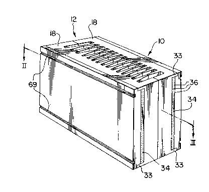
In the first embodiment as shown in Figure 1, an
electronic device 10, to be used as a single module in
conjunction with other modules in a support frame and
device combination, comprises a heat sink means 12 and two
electronic units comprising two printed circuit boards 14
(Figure 2) disposed one on each side of the heat sink
means. The embodiment also includes means for sealing the
printed circuit boards and electronic components carried
thereon from ambient atmosphere, the sealing means compris-
ing two planar covers 16, associated one with each of the
boards 14.
As is shown in Figures 1 and 2, the heat sink
means comprises two parallel spaced apart side walls 18
with two outwardly facing side surfaces 20 directed in
opposite directions from the walls 18. The heat sink means
2 ~ 7
12 is formed of two separate hea~ sink structures 22
(Figures 1 and 2), each of the structures 22 comprising one
of the walls 18 and end walls 24 and 26, the end walls
extending towards each other from one heat sink structure
to the other and into abutting relationship.
Each heat sink structure 22 is also provided with
integral heat release projection means in the form of
rectilinear and parallel ribs 28 which extend inwardly of
the heat sink means from the side walls 18 and lie between
lo the end walls 24 and 26. As may be seen from Figure 2, the
ribs 28 extend from the two heat sink structures 22 so as
to form rib pairs, from one heat sink structure to the
other, and free ends of the ribs oppose each other and lie
substantially in contact from one structure to the other.
The free ends of the ribs and the free ends of the end
walls 24 and 26 lie substantially on a common plane as
shown by the Figures. The arrangement of the ribs provides
a passage means for the flow of a cooling fluid, namely
air, between the ribs, the passage means being defined by
separate passages 30 defined by substantially contacting
pairs of ribs. In an alternative construction (not shown)
the heat sink means is formed as an integral structure with
the ribs 28 extending from one wall 18 completely across to
the other.
Each printed circuit board 14 has a plurality of
electronic components 31 o~ the respective electronic unit
extending outwardly from an electronic component bearing
surface of the printed circuit board to provide a heat
radiating side to the electronic unit. The sides 20 of the
heat sink structures 22 are basically planar and have
profiled surfaces as shown in Figure 2 which closely con-
form to the shapes of the electrical components while
providing a space between the profiled surfaces and the
components. This spacing is such that heat transfer will
occur from the electrical components and into the heat sink
structures 22. The profiled shape of each of the sides 20
is such that blind cavities 32 extending into each heat
10 2~ 07
sink structure have sides closely surrounding each of the
electronic components and the remainder of the original
planar surface of each side 20, into which the cavities are
formed contacts the prlnted circuit board and supports it.
This is as shown in Figure 2 in which, as can be seen from
that Figure, each of the cavities 32 is shaped individually
to suit its particular electronic component. It has been
found that the sides of the cavities 32 should be spaced
from their respective components from 0.5 to 2.0 mm to
lo obtain the most efficient transfer of heat energy into the
heat sink structures while insuring on a practical basis
that each of the components remains spaced from the sides
of its respective cavity.
The electronic components 31 mounted upon the
printed circuit board may be various shapes and sizes and
include any of the components which normally extend from
printed circuit board structures. In particular, it is
envisaged that chip capacitors or resistors may be included
in the embodiment and such capacitors or resistors may be
packaged or unpackaged. Any problems arising in use from
collecting dust upon such unpackaged resistors or any other
components 31 is avoided, because the two covers 16 seal
the printed circuit boards 14 and the components 31 com-
pletely from ambient atmosphere. For this purpose, each of
the heat sink structures 22 is provided with a flange 33
which extends outwardly along the top and bottom edges of
the structure (Figure 1) and down one side of the structure
(Figure 2) and these flanges extend outwardly from the heat
sink structure while being spaced from the edges of the
printed circuit board. Each cover 16 is mounted upon and
is sealed against the free ends of its flanges 33 so as to
prevent dust or other foreign particles from entering into
the electronic device and into contact the printed circuit
board and its components. Extending downwardly along one
edge of each of the printed circuit boards 14 is a con-
nector 34 which is connected to circuitry in the respective
printed circuit board 14. Terminals 36 of each of the
2~g ,t,.~07
ll
connectors are exposed at the end wall 26 of the respective
heat sink structure 22 with the connector side,s sealed
between its heat sink structure and its cover 16.
Further to illustrate the structure of the embodi-
5 ment, reference is made to Figure 3. This figure relatesto a theoretical struct:ure in which the design of the
printed circuit board and its electronic components is
simplified from that shown in the first embodiment, but
shows all of the essential features of that embodiment.
lo With regard to Figure 3, the same reference numerals are
used as in the first embodiment. In Figure 3, in which
only one printed circuit board is shown, each printed
circuit board 14 has components 31 which, for convenience,
are shown equally spaced apart and of the same size. A
15 connector 34 is mounted along one edge of the printed
circuit board as in the embodiment. The side 20 of the
wall 18 is formed with a plurality of cavities 32 of suf-
ficient size to provide the small clearance required
between the components 31 and the sides of the cavities
20 upon assembly. In Figure 3 and accompanying Figure 4, the
components 31 may readily be considered to represent un-
packaged chip capacitors or resistors which are assembled
directly onto the board 14. In Figure 3, the cover 16 is
shown disposed outwardly from the printed circuit board 14
25 in the exploded view. In the enlargement of Figure 4, each
of the components 31, e.g., unpackaged chips, has a space
40 between itself and the sides of its respective cavity
32. With the distance between each component 31 and the
sides of its cavity 32, i.e. across the space 40 being
30 suitable e.g. from 0.5 tG 2.0 mm, a high degree of heat
transfer from each component 31 into the heat sink
structures; results. In the case of unpackaged chips, heat
transfer is maximized because the chip structures are
undeterred by packaging. Leads 35 are shown dia-
35 grammatically from each component to the board 14.
With this structure, heat is extracted at a highlyefficient rate from each component, particularly so in the
2~ o~
12
case of the unpackaged chips which are exceedingly suscept-
ible to deleterious effects from high temperature condi-
tions.
In addition to protection against dust settling
upon the electronic components 31 together with its attend-
ant advantages, a further advantage is that, because the
printed circuit boards are surrounded by the closure and
the heat sink structures, an extremely effective EMI sup-
pression results.
o In Figure 4A which shows a modification of Figures
3 & 4, the cavities 32 are avoided and the side 20 of the
wall 18 projects outwards specifically towards each com-
ponent 31 so as to provide a protrusion which lies suffi-
ciently close to the component to provide for a high degree
of heat transfer across the space 40 between protrusion and
component.
The electronic device 10 described in the first
embodiment, together with a plurality of similarly con-
structed devices, is suitable for assembly into a support
frame 60 such as is described with reference to Figures 5
and 6. The frame 60 comprises two vertical main support
members 62 between which are disposed a plurality of
vertically spaced horizontal support platforms 64, having a
plurality of parallel rectilinear guiding supports 66
projecting upwardly and downwardly therefrom. The supports
66 are directed from the front 68 (Figure 6) to a rear 70
of the frame structure. The guiding supports 66 are of T
shape as shown by Figure 5 with the lower row of supports
being of inverted T shape and directly disposed beneath the
upper supports 66. Adjacent supports 66 are for sliding
reception within grooves 69 provided towards the top and
bottom edges of each of the closures 16, for instance as
shown in Figure 1, to enable each of the devices 10 to be
assembled into an indivldual receiving station in the frame
structure 60. As may be seen from the upper end of Figure
5, five units are disposed in this embodiment in horizontal
side by side relationship in respective receiving stations
13 2 ~ 3 0 7
in each of two vertically disposed rows of stations. In
the upper stations, the guiding supports 66 are located in
lower grooves 69 of the covers 16 while in the lower
stations the electronic devices 10 hang downwardly from the
s lower guiding supports 66 which are received in the upper
grooves 69 of the covers 16. Each support plate 64 is
formed with apertures (not shown) which coincide with the
passages 30 for upward flow of air upon assembly of the
electronic devices into the frame. As may be seen from
lo Figure 5, each of the devices 10 is mounted into the frame
by moving it into the front and towards the rear 70 of the
frame with the connectors 34 and their terminals 36 facing
forwardly. This is to allow for frontal access of each of
the printed circuit boards for connectorization purposes
and hence eliminates the need for the use of a backplane
which is conventional in printed circuit board technology
where boards are mounted side by side in frames as edge
cards.
With the electronic devices disposed in their
receiving stations as shown at the top part of Figure 5 and
also in Figure 6, the passages 30 for flow of air extend
upwardly between the ribs 28 and during use, the heat
generated by the electronic components 31 in each of the
devices 10 is transferred across the spaces 40 between the
electronic co~ponents and the surfaces of the cavities 32
so that it is readily transferred from the ribs 28 into the
cooling air flowing upwardly through the passages. The
design requirements are such that air is moved upwardly
naturally by convection as it is warmed in the passages 30
by the heat transfer so that cooling fans are not required.
Of course, with two or more of the electronic devices 10
arranged in vertical alignment in their respective
receiving stations as shown in Figures 5 and 6, then the
convection effect is increased so as to provide better
upward flow of air. The air is drawn into the frame struc-
ture through entrances 72 provided by box structures 74
having a lower sloping panel 76 and an upper horizontal
14 2 ~ 7
panel 78, the air moving upwardly through apertures in the
upper horizontal panel 78 disposed beneath the lower hori--
zontal row of electronic devices. The air exits from an
exit passageway 80 having an upper boundary provided by an
upper sloping panel 82 (Figure 6) and passes through an
interconnecting aperture 84 in a wall 86 upon which the
frame structure 60 ls mounted. The distance between the
inlet 72 and the exit 80 for the air is partly dependent
upon the amount of heat transfer which is required and may
lo be designed to accommodate air flow through one, two or
more horizontal rows of receiving stations. In Figure 6,
there are two horizontal rows of receiving stations, each
containing five electronic devices 10 between the inlet 72
and exit 80.
The electronic devices 10 have flat sides provided
by planar outer surfaces of the covers 16 to provide a
compact storage arrangement in the support frame structure
with the covers 16 of adjacent devices lying side by side
and in close proximity with each other. As may be seen,
because of the use of the covers, particularly in a sealing
capacity as described in the embodiment, it is impossible
for ambient air to contact the electronic components 31
carried by the printed circuit boards and, as indicated,
the performance of these components does not deteriorate
due to an accumulation of dust or foreign particles upon
them. In this embodiment, each device 10 which forms a
separate module, has approximate overall dimensions of 3.4
inches in width, a height of 7.4 inches, and a length of
8.8 inches between the ends of the device. Each device is
thus easily managed manually for insertion and removal
purposes and for general handling.
While the electronic components of the first
embodlment and according to the invention should preferably
be used with convected air, cooling fans may of course be
employed if deemed necessary. The covers 16 of each of the
devices 10 will, of course, still protect the electronic
15 2~ 7
components of the printed circuit boards from the effects
of dust or other foreign particles with use.
In the second embodiment illustrated by Figure 7,
an electronic device 90 has heat sink means comprising a
single heat slnk structure 22 instead of two mating struc-
tures as descrlbed in the first embodiment. In this second
embodiment, in which parts of the device are otherwise
similar to that described in the first embodiment, parts
similar to those described in the first embodiment will
lo bear the same reference numerals.
In the second embodiment the single heat sink
structure 22 supports a single printed circuit board 14
with its electronic components 31 mounted thereon and
extending into cavities 32. The printed circuit board 14
has a connector 34 with terminals facing outwardly from the
device and a closure 16 extends across the device outwardly
from the printed circuit board so as to seal together the
side 20 of the heat sink structure 22 from ambient atmos-
phere.
In use, the device 90 is suitable for mounting
upon a wall 92 in which the wall vertically defines con-
vection air passages 94 in association with the ribs 28 of
the heat sink structure 22.
In a third embodiment (Figure 8), an electronic
device 100 comprises a backplane 102 mounted upon the rear
wall of a closed box 104 having forwardly facing sides 106
and top and bottom (both not shown). Cables 107 extend
vertically behind the box.
Mounted upon the backplane 102 is an electronic
unit comprising a printed circuit board 108 lying parallel
to the backplane 102 and having connectors (not shown)
connected into terminals of the backplane. A heat radia-
ting surface of the printed circuit board is provided by
electronic components 110 facing forwardly from the board.
~ heat sink means for extracting heat radiated
from the electronic components comprises a door 112 which
is sealed around its edges, by a seal 114 to a continuous
16 ?.~ 7
planar flange 116 extending alony free edges of the sides
106 and top and bottom of ~he box 104. The door has heat
exchange projections 118 projecting forwardly from it and
the rear of the door has surface means close to the com-
ponents 110. The surface means comprises a plurality ofneedle-like horizontal projections 120 projecting rearwards
of the door. These projections terminate at their free
ends at posltions close to surfaces of the electronic
components which they approach so as to provlde a high heat
o transfer rate from the components, through the door and out
through the projections 118.
The door may be forwardly covered by a panel 122
which provides a vertical passage 124 for flow of cooling
air, by convection, upwardly of the passage and between a
lower inlet and upper outlet.