Note : Les descriptions sont présentées dans la langue officielle dans laquelle elles ont été soumises.
WO91/18279 2 0 8 3 5 ~ 9 PCT/US91/03598
GAS ANALYZERS
TECHNICAL FIELD OF THE INVENTION
In one aspect the present invention relates
to novel, improved, transducers for non-dispersive
infrared radiation (NDIR) gas analyzation.
In second aspect, the present invention
relates to transducers of the character just described
which are usable in conjunction with an airway adapter
to measure the concentration of a specified gas
flowing through the adapter.
In a third respect, the present invention
relates to novel, improved devices for emitting energy
in the infrared part of the electromagnetic spectrum.
In yet another aspect, the present invention
relates to power supplies and, more particularly, to
novel, improved power supplies of the bipolar type.
In a related aspect, the present invention
relates to non-dispersive infrared radiation (NDIR)
transducers which have infrared radiation emitters
driven by bipolar power supplies embodying the princi-
ples of the present invention.
The present invention also relates to
detectors and, more specifically, to novel, improved,
infrared radiation detector units.
BACKGROUND OF THE INVENTION
30~ V.S. patents Nos. 4,859,858 and 4,859,859,
-- both entitled GAS ANALYZERS, were issued to Knodle et
al. on 22 August 1989. Both patents disclose state-
of-the art apparatus for outputting a signal indica-
2 ~3509
tive of the concentration of a designated gas in a sample beingmonitored by the apparatus.
The gas analyzers disclosed in the '858 and '859 patents
are of the non-dispersive type. They operate on the premise that
the concentration of a designated gas can be measured by: (1)
passing a beam of infrared radiation through the gas and (2) then
ascertaining the attenuated level of the energy in a narrow band
absorbable by the designated gas. This is done with a detector
capable of generating a concentration proportional electrical
output signal.
One important application of the invention at the
present time is in capnometers for monitoring the level of carbon
dioxide in the breath of a medical patient. This is typically
done during a surgical procedure as an indication to the
anesthesiologist of the patient's condition, for example. As the
patient's well being and even his life, is at stake, it is of
paramount importance that the carbon dioxide concentration be
measured with great accuracy.
In a typical instrument or system employing
non-dispersive infrared radiation to measure gas
concentration, including those disclosed in the '858
and '859 patents, the infrared radiation is emitted
from a source and focused by a mirror on the gases
being analyzed. After passing through the body of gases, the
beam~of infrared radiation passes through a filter. That filter
absorbs all of the radiation except for that in a narrow band
centered on a frequency which is absorbed by the gas of concern.
This narrow band of radiation is transmitted to a detector
. . ,
WO 91 /1 8279 PCr/l lS91 /03598
~31~ ~ 9
which is capable of producing an electrical output
signal proportional in magnitude to the magnitude of
the infrared radiation impinging upon it. Thus, the
radiation in the band passed by the filter is attenu-
ated to an extent which is proportional to the concen-
tration of the designated gas. The strength of the
signal generated by the detector is consequently
inversely proportional to the concentration of the
designated gas and can be inverted to provide a signal
lo indicative of that concentration.
While a non-dispersive analyzer must be
tailored to the specific gas of interest, it is
typically small, relatively cheap, and rugged enough
to be used in medical and other demanding environ-
15 ments.
Of considerable, if not critical, importancein apparatus and systems of the character just de-
scribed is the source or emitter which produces the
beam of infrared radiation.
Infrared radiation sources that are specifi-
cally designed for non-dispersive gas analyzers or
that would appear to be useful in such equipment are
disclosed in the following U.S. patents:
Patent Issue
Number Patentee(s) Date
3, 694, 624 Buchta 26 Sep. 1972
3,875,413 Bridgham 01 Apr. 1975
4,378,489 Chabinsky et al. 29 Mar. 1983
4,620,104 Nordal et al. 28 Oct. 1986
4,914,i20 Knodle et al. 03 Apr. 1990
Infrared radiation sources as disclosed in the
foregoing patents, as well as those disclosed herein,
can also be used for a variety of other purposes.
W O 91/18279 P ~ /US91/03598
2~5~
Irrespective of the end use, heretofore available
infrared sources of the character disclosed in the
above-cited patents have a number of drawbacks.
One is that the temperature to which such
sources can be heated is often relatively low.
Because the output of an infrared source is directly
related to the temperature to which it is heated, the
output of such sources is low; and this may make such
sources impractical for many applications.
Also, in those non-dispersive gas analyzers
disclosed in the '858 and '859 patents, the emitter
has a substrate of a material with low thermal conduc-
tivity such as steatite. Two T-shaped conductors or
termi~als are bonded to the upper surface of the
substrate in spaced relationship; and a film of an
emissive, electrically resistive material is superim-
posed on the conductors and bonded to the upper
surface of the substrate with its ends overlapping and
electrically connected to the conductors. This
emitter is attached to posts at its opposite ends and
supported by those posts from a metallic emitter mount
with the emissive film facing the mount. That com-
ponent has a polished, parabolic, mirror surface
formed in the surface which the emitter faces. This
mirror collimates the emitted infrared radiation and
focuses the collimated radiation into a beam directed
along the optical path of the device or system in
which the infrared radiation source is employed.
In the previously disclosed infrared radiation
sources, the substrate bearing the emissive film was
fixed at both of its ends to the supporting posts. As
the substrate was heated by the emissive film, it yrew
or increased in length due to thermal expansion. This
WO 91/18279 PCI tUS9 1/03598
208~509
has led to failure of the patented type of infrared
radiation source because of the stresses that were
consequently imposed on the substrate and substrate-
supported components.
Furthermore, assembly of the patented infrared
radiation sources is somewhat com~licated and exact-
ing. For these and other reasons, the patented
sources may prove to be somewhat less than optimal in
applications where a high quality, yet inexpensive,
infrared radiation source is required.
For a gas analyzer of the NDIR type to operate
efficiently, the infrared radiation passed through the
gas undergoing analysis must be of a modulated or
pulsed character. That is, it must be made available
as a stream of pulses rather than in the form of a
continuous beam. Otherwise, the signal-to-noise ratio
of the electrical signal available from the analyzer
will typically not be high enough for the signal to be
useful.
Two methods for supplying modulated infrared
radiation to the environment in which sampling occurs
have heretofore been proposed. One employs a mechani-
cal chopper to create the wanted stream of pulses from
a continuous beam of energy outputted by the infrared
radiation source. A chopper has a spinning wheel
between the infrared radiation source and the detec-
tor. The wheel has a series of apertures spaced
equally around its periphery. Consequently, as the
wheel rotates, the transmission of the attenuated beam
of infrared radiation to the detector of the gas
analyzer is alternately enabled and interrupted,
typically at a frequency of less than one hundred
cycles per second.
WO9l/18279 PCT/US9l/03598
2083~09
-
Gas analyzers of the character just described
are disclosed in U.S. Patents Nos.: 3,793,525 issued
February 19, 1974, to Burch et al. for DUAL-CELL NON-
DISPERSIVE GAS ANALYZER; 4,811,776 issued May 21,
1974, to Blau, Jr. for GAS ANALYZER; 3,987,303 issued
october 19, 1976, to Stoft et al. for MEDICAL ANALYTI-
CAL GAS DETECTOR; 4,011,859 issued March 15, 1977, to
Frankenberger for METHOD FOR CONTINUOUSLY MEASURING
THE C02 CONTENT IN BREATHING GAS; 4,204,768 issued May
27, 1980, to N'Guyen for GAS ANALYZERS OF THE SELEC-
TIVE RADIATION ADSORPTION TYPE WITH A CALIBRATION
CELL; 4,268,751 issued May 19, 1981, to Fritzlen et
al. for INFRARED BREATH ANALYZER; AND 4,371,785 issued
February 1, 1983, to Pedersen for METHOD AND APPARATUS
FOR DETECTION OF FLUIDS and in A Reliable, Accurate
C~2 Analyzer for Medical Use, Solomon, HEWLETT-PACKARD
JOURNAL, September 1981, pages 3-21.
Gas analyzers with mechanical choppers have a
number of drawbacks. They are bulky, heavy, and
expensive; have moving parts, which is undesirable;
and also have complex optical designs. They also tend
to be less accurate than is desirable and to lack long
term stability.
Also, gas analyzers employing mechanical
choppers are relatively fragile. For example, they
will typically not work properly, if at all, after
they are dropped.
A second, and believed superior, method of
generatlng the necessary modulated infrared radiation
is to drive the infrared radiation emitter with a
- power supply which applies pulses of electrical energy
to the emitter. In an NDIR analyzer with the type of
infrared radiation emitter described above, an emis-
WO91/18279 PCT/US91/03598
20835~9
sive layer of the emitter heats up and emits a pulseof infrared radiation when a pulse of electrical
energy is applied to that layer by the power source.
Thereafter, the emissive layer rapidly cools down.
s Therefore, in the remainder of the emitter duty cycle,
radiation in the infrared portion of the spectrum is
not outputted from the emitter to any appreciable
extent.
This modulation ~Pchnique has the advantage of
eliminating mechanical systems and components along
with the attendant bulk, weight, complexity, and
fragility of those devices. Also, the pulsed power
supply approach tends to be significantly more ac-
curate than the m~r~nical chopper technique.
Heretofore, the power supplies used for the
purposes just discussed and in similar applications
supplied unipolar p~ ~c of controlled magnitude,
duration, and frequency to the driven emitter -- that
is, a stream of pulses all having either a positive
(or negative) value. As a result, pulsed emitters
tend to have an important disadvantage common to
schemes employing mechanical choppers, a lack of long-
term stability. This is a result of the operating
current always flowing in the same direction through
the emitter and producing strong electrical fields.
These, because they are all oriented in the same
direction, cause migration of the emitter materials
over time. The consequence of that migration is
degraded performance and, ultimately, failure of the
emitter.
In a typical instrument or system employing
non-dispersive infrared radiation to measure gas
concentration, including those disclosed in the '858
WO 91/18279 PCI /I 'S91 /03598
2083509
and '859 patents, the infrared ra~iation is emitted
from a source and focused by a mirror on the gases
being analyzed. After passing through the body of
gases, the beam of infrared radiation passes through
a filter. That filter absorbs all of the radiation
except for that in a narrow band centered on a fre-
quency which is-absorbed by the gas of concern. This
narrow band of radiation is transmitted to a data
detector which is capable of ~ducing an electrical
output signal proportional in magnitude to the magni-
tude of the infrared radiation impinging upon it.
Thus, the radiation in the band passed by the filter
is attenuated to an extent which is proportional to
the concentration of the designated gas. The strength
of the signal generated by the data detector is
consequently inversely proportional to the concentra-
tion of ~he designated gas and can be inverted to
provide a signal indicative of that concentration.
While a non-dispersive analyzer must be tai-
lored to the specific gas of interest, it is typicallysmall, relatively cheap, and rugged enough to be used
in medical and other demanding environments.
Most non-dispersive infrared gas analyzers use
a ratioing scheme to eliminate errors attributable to
drifts in the infrared source and other parts of the
system and transmission losses. Two methods are
common.
1. An optical chopper is used with a single
detector. The chopper contains a reference cell or
filter, and the detector signal alternates between
that reference cell and the gas to be measured. A
ratio is taken of these two signals.
W O 91/18279 2 0 8 3 S 0 9 P ~ /US91/0359X
2. Two detectors are located next to each
other, and each is illuminated by one-half of the
infrared beam. A ratio is taken of the two detector
outputs. The reference channel is presumed to be
responsive to any changes in the detected energy that
are not due to the absorption of the designated gas,
and the changes are presume~ to be the same in both
the reference and data channels.
A major drawback of the optical chopper tech-
nique is that it requires a device with moving partsto implement it. Such devices tend to be expensive,
bulky, and fragile and to require frequent calibra-
tion.
Another difficulty, common to both schemes, is
that the ratioed signals are different in time in the
first case and different in space in the second.
These differences can produce a false signal from the
detector if there are time variations in the first
case or spatial variations in the second case.
Also, any motion in the system can cause time
and spatial variations in the infrared radiation beam.
At best, this can require frequent recalibration.
Recalibration is time consuming and expensive and
takes the unit or system out of operation which may be
unacceptable -- for example, a major surgical proce-
dure cannot be interrupted simply to recalibrate an
instrument.
Dispersive infrared analysis is also utilized
to measure the concentration of a designated gas in a
stream or other sample being analyzed. In this
approach, a broad band of energy is transmitted
through the gas, then through a dispersive element,
typically a prism or a diffraction grating. The
WOgl/18279 PCT/US91/03598
20835~9
dispersive element spreads out the energy according to
wavelength. The intensity of the energy will vary
across that space depenAing on the absorption charac-
teristics of the gas under analysis.
A detector scans through a large range of
wavelengths, thereby recording intensity (i.e.,
absorption of the gas) as a function of wavelength.
A manual or electronic examination of this recording
will identify the gas or gases that may be present.
The detector can also be fixed in space, thus record-
ing the intensity of a particular wavelength (and gas)
of interest.
The dispersive type of gas analyzer is espe-
cially useful where an unknown gas may be present
~ecause a very larqe range of wavelengths can be
covered. It is also useful where there are several
gases present.
The dispersive analyzer is flexible and can be
very accurate, but it is expensive and bulky. It i8
most often found in a laboratory, and it i8 not at all
suitable for applications ~uch as those medical
applications in which the entire emitter/detector
system may have to be suspended in the plumbing
between a patient and a mech~nical ventilator, for
example.
A number of U.S. patents disclose optical
systems which: (1) have detectors and beam splitters,
and (2) are intended for purposes at least generally
comparable to those disclosed herein. They are:
Patent
Number Patentee(s) Issue Date
2,737,591 Wright et al. 06 March 1956
3,004,664 Dreyfus 17 October 1961
WO91/18279 PCT/US91/03598
20835D9
3,287,556 Good 22 November 1966
3,811,776 Blau, Jr. 21 May 1974
3,821,553 French 28 June 1974
3,916,195 Burch et al. 28 October 1975
4,410,273 Mantz et al. 18 October 1983
4,468,561 Speeter 28 August 1984
4,536,090 Schmidt et al. 20 August 1985
None of the foregoing patents are concerned
with a detector unit or system which the highly
desirable attribute of interchangeability.
Nor, with the possible exception of Good's, do
the patented systems make use of a beam splitter which
is capable of resolving a beam over its entire compass
into energy which is respectively above and below a
selected wavelength. And, even Good only discloses
that this can be done with his beam splitter if the
inputted energy is coherent. This requirement for
laser generated energy would make the Good system too
complicated, bulky, and expensive for at least many of
the applications for which the novel detector units
and systems disclosed herein are ~o well suited.
Furthermore, Good has not disclosed how this patented
system could be constructed to meet the FDA (Food and
Drug Administration) requirements for Class III
lasers. Absent FDA approval, the system would of
course have the disadvantage of being of no signifi-
cant practical value.
SUMMARY OF THE INVENTION
Now invented, and disclosed herein, are certain
new and novel infrared radiation emitters, power
supplies, and detector components which are free of
Wo9l/l8279 2 0 8 3 5 ~ 9 PCT/~lS91/03598
the drawbacks of those components of the same charac-
ter discussed above. These novel components are
particularly well suited for NDIR gas analysis but can
also be used to advantage in other applications.
The infrared radiation sources disclosed herein
have all of the capabilities of those described in the
'858 and '859 patents. However, they also have a
number of important advantages which the patented
infrared radiation sources do not have.
Briefly, the novel infrared radiation sources
of the present invention are like those disclosed in
the '858 and '859 patents in that they have a low
thermal conductivity substrate supporting a film-type
emissive element. However, they differ in one impor-
tant respect in that the ends of the substrate are not
fixed at an invariable distance relative to each
other. Instead, one end is fixed to a commutator,
which serves as a support for the substrate-based
emitter component; and the opposite end of the sub-
strate is left free to move relative to the com-
mutator. Consequently, the substrate is free to grow
in length as its temperature increases; and the
imposition of mechanical stresses on the emitter unit
is thereby avoided.
The commutator-based approach also facilitates
assembly. For example, electrical connections are
easier to make (and also less apt to break); and the
need for insulated leads is eliminated. Also, the
film-type emissive element is automatically centered
on the axis of the energy collimating and focusing
mirror. This simplifies, and reduces the cost of, the
assembly process by eliminating the steps heretofore
W O 91/18279 P ~ /US91/03598
2U83509
employed to insure that the emissive element was
accurately aligned with the collimating mirror.
Furthermore, the components of the herein
disclosed infrared radiation sources are primarily
molded from plastics rather than being machined from
metal as in the patented sources. This allows an
acceptable degree of accuracy to be maintained while
significantly reducing the cost of the parts.
In addition, the novel design of the herein
lo disclosed infrared radiation sources allows the
collimating mirror to be assembled last. This mini-
mizes the possibility that the mirrored surface might
be scratched or otherwise damaged. That is important
because the mirror is the most expensive part of the
infrared radiation source.
Yet another, very important advantage of the
infrared radiation sources disclosed herein is that
the thermal, physical, electrical, and other paramete-
rs of the emissive element, the electrical conductors
through which current flows to the emissive element,
the substrate supporting the emissive element, and
even the substrate-mounting components are so balanced
and correlated that the flow of heat away from~ the
operating emissive element is closely controlled and
correlated with the emitted infrared energy. This
results in an infrared radiation source which can be
made to emit infrared radiation of accurately predic-
table intensity. This is important. For example, it
is the difference in intensity between emitted and
detected energy in appropriate band widths that is
employed by non-dispersive gas analyzers as a measure
of the concentration in a sample of the gas being
WO9l/18279 PCT~US91/03598
20835~9
monitored; and this differential i~ not accurate if
the intensity of the emitted radiation i~ not.
The above-described and unwanted migration of
materials in those infrared radiation emitters having
an emissive layer on a compatible ~ubstrate can be
avoided in accord with the principles of the present
invention by-employing a bipolar power source, instead
of a unipolar one, to drive the emitter of an infrared
radiation source. By doing so, the electrical fields
created in the vicinity of the emitter are reversed
each time operating voltage i8 applied to the emitter;
and the tendency of the emitter materials to migrate
is eliminated.
Yet another advantage of employing a bipolar
power supply to operate an infrared radiation emitter
of the character described above is that more power
can be applied to the emiseive component of the
emitter; i.e., higher current densities can be employ-
ed. This is important because the result is increased
emitter output.
Also, higher frequencies can be employed. And,
because migration ceases to be a significant problem,
emitter materials heretofore ruled out because of
susceptibility to migration but otherwise desirable
can be employed.
For the exemplary NDIR application discussed
above, the bipolar power supply is designed to output
pulses at a frequency in the range of 40 to 250 Hz and
at a voltage in the range of 12 to 24V with the pulse
taking up from 5 to 20 percent of the duty cycle.
Major components of the power supply are: a
driver which supplies the positive and negative
pulses; timing circuits that control the frequency
W O 91/18279 P(~r/US91/03598
20835~9
with which the pulses are outputted by the driver;
watchdog circuits for shutting down the driver lf a
fault occurs; and a reset circuit which delay~ Fubse-
quent restarting of the driver once the fault i6
cleared. The reset circuit allows the timing and
other circuits of the power supply to stabilize before
the outputting of emitter operating pulses is resumed.
The novel power supplies disclosed herein also
have the advantage that they can be used in many
applications other than the one just described. For
example, the infrared emitters of thermal printers
have the same material migration problem as the
emitters of gas analyzers. This problem can similarly
be solved by substituting a bipolar power supply of
the character described herein for the unipolar power
supplies heretofore employed to drive a thermal print
head.
Still other applications of these novel power
supplies, many not involving the operation of infrared
radiation emitters, will be readily apparent to those
to whom this specification is directed.
The new and novel infrared radiation detector
units disclosed herein, when employed in the non-
dispersive measurement of a designated gas, make it
possible to do this more accurately than is believed
to have heretofore been possible by way of that
approach. This is a significant advantage, especially
in medical and other applications where a ~igh degree
of accuracy is of the utmost importance. At the same
time, and unlike dispersive-type analyzers, these
novel detector units and systems are compact and
rugged enough for the most demanding applications and
are relatively inexpensive to produce.
WO91/1X279 PCT/US91/03598
~083509
Increased accuracy i~ achieved, in accord with
the principles of the present invention, by a novel
beam splitter which divides the energy over the entire
compass of a beam passed through gases being analyzed
into moieties in which the energy is of wavelengths
that are respectively shorter and longer than a
designated wavelength. The energy in these moieti-es
is transmitted through appropriate bandpass filters to
data and reference detectors of like dimensions which
are positioned in mirror image relationship to the
beam splitter. Consequently, both detectors receive
energy of appropriate wavelengths from all parts of
the beam. This eliminates the inaccuracies which
occur in side-by-side and other detector systems in
which: (l) the image of the beam falling on the
detectors is different in space because the data and
reference detectors are not spatially coincident,
and/or (2) different in time because the beam reaches
the data and reference detectors through first one and
then the other of the bandpass filters in front of
those detectors.
A novel, monolithic, isothermal mount supports
the beam splitter and the reference and data detectors
with the precision required for optimal accuracy.
Light traps associated with the mount keep extraneous
energy from reaching the detectors, providing a
further increase in accuracy.
Associated with the detectors is an onboard
power supply. The power supply output voltage is used
to bias the detectors; and, because the output is
precisely regulated, this is done essentially without
the inaccuracies in the outputs from the data and
WO9l/18279 PCT/US9t/03598
2083509
reference detectors that would occur if the biasing
voltage fluctuated.
Lead selenide-type detectors are preferred
because of their sensitivity and consequent capability
for accurately reflecting the magnitude of the infra-
red radiation falling ~n them. However, this means
that they are equally sensitive to variations in-
temperature. Therefore, even minor fluctuations in
the detector temperature and minor differences between
the temperatures of the data and reference detectors
can markedly affect accuracy.
A sensor/heater system promotes accuracy by
heating the isothermal support in a manner that keeps
the two detectors precisely at a selected temperature,
typically with a variation <O.Ol C. The support is
fabricated from a heat conductive material and so
configured as to reduce to this very small value the
temperature difference between the data and reference
detectors. At the same time, the novel, monolithic
detector supports and other hereinafter discussed
features of the devices make them rugged, but still
compact.
Also incorporated in the detector unit are a
pair of electronic amplifiers. These increase the
outputs from the data and reference detectors to
levels at which they can be transmitted without
excessive noise to a signal processor. The signal
processor converts the detector outputs to a signal
reflecting the concentration of the selected gas in
the stream or other sample being analyzed.
Typically, detector units of the character
disclosed herein are employed in environments in which
electrical noise is prevalent. A novel electrostatic
W O 91/18279 PC~r/~'S91/03598
208350~
shield effectively isolates the data and reference
detectors and associated circuitry from the adverse
effects of EMI and other radiations in the ambient
surroundings.
A novel casing houses the electrostatic shield
and the detectors and other electrical and optical
components of the detector unit and keeps foreign
matter from reaching those components. Guide systems
in the casing and in the electrostatic shield facili-
tate the assembly of the unit and the electrical
connection of the electrostatic shield to the compo-
nents shielded by that device.
The casing in which the detector unit is housed
may be one component of a transducer which also
includes a source as described above with components
for: emitting infrared radiation focusing that energy
into a beam, and propagating the beam through the
gases being analyzed. In applications of the inven-
tion which are of particular interest at the present
time, these transducers are used with an airway
adapter to measure the concentration of a gas such as
carbon dioxide flowing through the adapter.
These airway adapters are typically disposable,
and optical characteristics may vary from one adapter
to the next. This, however, is inconsequential, and
interchangeability is provided, when a detector unit
of the character disclosed herein is employed in the
transducer. Because both the data and reference
detectors of such units react to the energy over the
same compass of the attenuated beam, optical varia-
tions -- and others including drift, foreign substanc-
es in the optical path, etc. -- affect both detectors
in the same manner and to the same extent. Therefore,
WOgl/18279 PCT/US9l/0359X
208350~
anomalies are canceled out when the data and reference
detector outputs are ratioed. This also means that
the frequent recalibration required in other non-
dispersive, dual detector systems is unnecessary or,
at worst, minimized.
Preferably, a second system independent of that
utilized to control detector temperatures is employed
to keep the casing of the airway adapter at an elevat-
ed temperature (preferably in the 42-45-C range).
lo This is high enough to keep moisture from condensing
on those windows incorporated in the adapter to pass
the radiant energy into that device and, after it has
passed through the gas being analyzed, to the detector
system. This approach to eliminating the problems
that condensation might cause has the important
advantage that heating the airway adapter has no
effect on the power supplied to the data and reference
detector heaters. Consequently, the fluctuations in
the detector heater power supply that would occur as
the casing heats up if the casing heater and detector
heater circuits were tied together are eliminated. So
are the unwanted changes in detector temperature that
would be caused by such fluctuations.
OBJECTS OF THE Ih~;NlloN
~ rom the foregoing, it will be apparent to the
reader that one important and primary object of the
present invention resides in the provision of novel,
improved gas analyzsis transducers of the NDIR type.
A related and also important object of the
invention is to provide transducers having components
of the character specified in the objects which follow
-
WO 91/18279 PCI /1,'S9 1/03598
2083509
, .
and with the attributes and advantages elucidated in
those objects.
Another important and primary object of the
invention resides in the provision of novel, improved,
infrared radiation sources.
Related and also important but more specific
objects of the present~invention reside in the provi-
sion of infrared radiation sources:
which are unlikely to fail because of the
thermally induced growth of a substrate supporting the
emissive element of the device;
which have a construction such that the emis-
sive element of the device is automatically aligned in
the course of assembling the device with a mirror
employed in the device to collimate and focus the
emitted radiation;
which facilitate the making of electrical
connections and eliminate the requirement that insu-
lated wire be employed for this purpose;
20which are made up of parts that can be inexpen-
sively yet accurately fabricated and easily assembled;
which can be assembled in a manner that protec-
ts the most expensive part of the device -- a col-
limating and focusing mirror -- from damage by allow-
ing it to be assembled last;
which are capable of emitting infrared radia-
tion of accurately predictable intensity.
Still another important and primary object of
the invention resides in the provision of novel
methods for assembling an infrared radiation source or
unit of the character identified in the preceding
objects.
WO 91/18279 PCltUS91/03598
2083509
A further important and primary object of the
invention resides in the provision of novel, improved,
electronic power supplies.
A related and also important object of the
invention resides in the provision of power supplies
which have a bipolar mode of operation in that they
are capable of outputting pulses which alternate in
polarity.
An object which is also important and related
to the previous one resides in the provision of
bipolar power supplies which can be used to advantage
in a variety of applications.
Still another related and important object of
the invention is the provision of electronic power
1~ supplies which can be employed to particular advantage
to drive infrared radiation emitters, especially those
with a substrate supporting a layer of an emissive,
electrically resistive material.
Yet another important object of the invention
is the provision of novel methods of operating the
infrared radiation emitters of gas analyzers and other
devices and systems, those methods involving the
application of pulses which alternate in polarity to
the emissive element of the emitter.
A still further important and primary object of
the present invention resides in the provision of
novel units or systems for detecting energy in the
infrared portion of the electromagnetic spectrum.
Other, related and also important but more
specific objects of the invention reside in the
provisions of systems as characterized in the preced-
ing object:
-
WO 91J18279 PCI/US91/03598
2083509
which are particularly useful in non-dispersive
gas analysis to generate a reference signal and a
signal indicative of the concentration of a selected
gas in a sample being analyzed;
S which are compact and rugged and therefore
particularly well suited for field use in medical and
other demanding applications;
which do not require the frequent recalibration
heretofore needed in non-dispersive systems to compen-
sate for accumulations of energy absorbing foreign
substances on optical components of the system;
which are extremely accurate due to a novel
arrangement for precisely aligning the optical compo-
nents of the system;
in which accuracy is promoted by a novel
arrangement for keeping the detectors of the system --
a reference detector and a data detector -- at the
same, selected temperature;
which have a beam splitter that directs incom-
ing infrared radiation to the reference and data
detectors and differs from conventional beam splitters
in that all of the incoming energy in a band absorbed
by a selected gas of interest is directed to the data
detector and in that the remainder of the incoming
energy over the same compass of the beam is directed
to the reference detector so that both detectors
respond to the same compass of the incoming beam,
thereby increasing the accuracy of the system;
in which accuracy is promoted by a novel system
for electrostatically shielding the operating compo-
nents of the system;
which have in~egral circuitry for amplifying
the signals outputted from the reference and data
WO 91/18279 ~Cl /US91/03598
20B3~ 09
detectors and thereby reducing the effect of noise on
those signals;
which have integral circuitry for amplifying
the signals outputted from the reference and data
detectors and thereby reducing the effect of noise on
those signals;
which have traps that keep extraneous electro-
magnetic energy from reaching the reference and data
detectors;
which are easily assembled in a transducer that
also has an infrared radiation source and in a manner
that facilitates the making of subsequent electrical
connections among the assembled components;
which have a novel housing construction that
isolates optical components from the surrounding
environs to prevent contamination, yet allows infrared
radiation to reach those components without interfer-
ence;
which can be sued in a variety of applications
and to measure the concentrations of many different
gases; and
which, in conjunction with the foregoing
object, can advantageously be employed in conjunction
with an airway adapter to accurately measure the
concentration of a designated gas flowing through the
adapter.
Objects related to those just expressed include
the provision of detector units and systems:
which remain accurate as another airway adapter
is substituted for the preceding one even though the
optical characteristics of those adapters -- including
dimensions -- may vary;
Wogl/18279 PCT/US91/03598
2083509
24
which have associated therewith a system for
heating the airway adapter casing to a temperature
high enough to keep moisture from forming on the
casing and interfering with the accuracy afforded by
the detector system;
in which, in conjunction with the preceding
object, independently controlled systems are employed
~o heat: (a) the airway adapter casing, and (b) the
data and reference detectors so that the heating of
the airway adapter casing does not introduce inaccura-
cies into the signals outputted by the detectors.
Other important objects and features and
additional advantages of the invention will be appar-
ent to the reader from the foregoing and the appended
claims and as the ensuing description and discussion
proceeds in conjunction with the accompanying draw-
ings.
BRIEF DESCRIPTION OF THE DRAWINGS
In the drawings:
FIG. 1 is an exploded view of: (a) an airway
adapter which provides a particularized flow path for
a gas being analyzed, and (b) a transducer which
outputs a signal indicative of the concentration of
the designated gas in the mixture and a reference
signal; that transducer includes an infrared radiation
source or emitter unit constructed in accord with the
principles of the present invention;
FIG. 2 is a section through, and depicts, a
detector-incorporating optical system of the airway
adapter/transducer assembly;
W O 91/18279 P ~ /US91/03598
2083509
FIG. 3 i5 an exploded view of the infrared
radiation source;
FIG. 4 is a second exploded view presented to
show the relationship between: ~a) a commutator
employed in the infrared radiation source to ~ort
an infrared radiation emitter and to make electrical
connections~to that emitter unit, and (b) a molded
ring which supports the commutator and is the base of
the infrared radiation source;
FIG. 5 is a plan view, prior to its being
installed in the base, of an assembly made up of the
infrared radiation emitter and the supporting commuta-
tor;
FIG. 6 is a fragmentary, pictorial view of the
emitter/commutator assembly; this figure shows a novel
floating relationship between the emitter and the
commutator which allows the emitter to freely grow in
length as the emitter temperature increases, thereby
eliminating the imposition of ctresses which might
damage the emitter or electrical connections to that
unit;
FIG. 7 is a vertical ~ection through a parabol-
ic mirror component employed in the infrared radiation
source to collimate, focus into a beam, and direct
along a specific optical path infrared radiation
outputted by the emitter;
FIG. 8 is a plan view of the assembled source
or device;
FIGS. 9 and 10 are sections through the device
taken essentially along lines 9-9 and 10-10 of FIG. 8;
FIG. lOA is a cross-section through the emitter
of the infrared radiation source, showing the heat
path through that component;
WO91/18279 PCT/US9l/03598
20~3~-09
26
FIG. 11 is an elevation of a second infrared
radiation source also embodying the principles of the
present invention;
FIG. 12 is a second elevation of the source
shown in FIG. 11, in this ca~e looking in the direc-
tion indicated by arrows 13-13 in FIG. 12;
FIG. 13 is a section through the infrared
radiation source shown in FIG. 11, taken substantially
along lines 14-14 of FIG. 12;
FIG. 14 is a section through the source of
FIG. 11, taken substantially along line 15-15 of
FIG. 15;
FIG. 15 is a section through the source, taken
substantially along line 16-16 of FIG. 11;
1~ FIG. 16 is a fragmentary plan view of a com-
mutator component employed in the device of FIG. 11;
FIG. 17 is a vertical ~ection through a parabo-
lic mirror component employed in the infrared radia-
tion source of FIG. 11 to collimate, focus into a
beam, and direct along a specific optical path infra-
red radiation outputted by the emitter;
FIG. 18 is a block diagram of a bipolar power
supply employed in the transducer of FIG. lj
FIG. 19 shows the relationship among FIGS. l9A,
25 l9B, and l9C which together constitute a schematic
diagram of the bipolar power supply;
FIGS. 20-23 are timing diagrams which facili-
tate an understanding of the manner in which the power
supply operates;
FIG. 24 shows the relationship between FIGS.
24A and 24B which, together, constitute an exploded
view of the transducer of FIG. 1;
27
20 8 3~5 0 9 ~
FIG. 25 is a fragmentary view of the transducer,
partially assembled and showing the manner in which a printed
circuit board in a detector unit incorporated in the transducer is
connected up to an electrostatic shield in the transducer;
FIG. 26 is a fragmentary view of the detector unit,
taken along line 26 - 26 of FIG. 2 to facilitate an understanding
of the manner in which certain light traps incorporated in the
detector unit function;
FIG. 27 (appearing with FIGS. 10 and lOA) is a
fragmentary view of the front surface of the beam splitter taken
along line 27 - 27 of FIG. 2;
FIG. 28 is a fragment of FIG. 2, drawn to a larger scale
to better show a detector mounting system which electrically
isolates data and reference detectors of the detector unit from
their support;
FIG. 29 is a plan view of the reference detector,
looking in the direction of arrows 29 - 29 in FIG. 28;
FIG. 30 is a longitudinal section through the detector
unit;
FIG. 30A is a schematic of systems employed in the
detector unit to keep the data and reference detectors at the
same, selected, unvarying temperature and to keep the casing of
the airway adapter at an elevated temperature;
FIG. 31 is a block diagram of a system employed in the
transducer to supply power at appropriate voltages to the
electrical components of the transducer and to amplify the signals
outputted by the reference and data detectors;
FIG. 32 is an electrical schematic of a reference
detector amplifier employed in the system shown in FIG. 31;
A
WO91/18279 PCT/~'S91/03598
2~183509
28
FIG. 33 is an electrical schematic of a data
detector amplifier employed in the system shown in
FIG. 3l;
FIG. 34 is an electrical schematic of a power
supply incorporated in the system of FIG. 3l to
provide the requisite operating voltages;
FIG. 35 is a schematic view of the detector
unit optical system with the beam splitter employed to
direct energy of different wavelengths to the data
detector and the reference detector properly aligned
relative to the detectors;
FIG. 36 is a similar schematic but with the
beam splitter and detectors misaligned;
FIGS. 37 and 38 are graphs of data obtained
from knife edge scans of detector units with mis-
aligned and properly aligned optical components; a
comparison of these two figures makes evident the
degradation in performance attributable to optical
misalignment;
FIGS. 39 and 40 are plots of the raw data
obtained from the knife edge scans;
FIG. 41 is a graph showing the effect of
temperature on the dark resistance output of the data
and reference detectors; and
FIG. 42 is a section through a second type of
detector unit embodying the principles of the present
invention.
29 a 0 8 ~ 5 0 Q
DETAILED DESCRIPTION OF THE INVENTION
The principles of the present invention can be employedto particular advantage in transducers for outputting: (a) a
signal proportional in magnitude to the concentration of carbon
dioxide flowing through an airway adapter in a patient-to-
mechanical ventilator circuit and (b) a reference signal. These
signals can be ratioed in the manner disclosed in abovenoted U.S.
patents 4,859,858 and 4,859,859 to provide a third signal
accurately and dynamically representing the concentration of the
carbon dioxide flowing through the airway adapter. A
representative and preferred airway adapter and a complementary
transducer constructed in accord with and embodying, the
principles of the present invention are shown in FIGS. 1 and 2 and
respectively identified by reference characters 22 and 24.
FIG. 1 shows primarily the polymeric housing 26 of
transducer 24. This transducer also includes: (a) an infrared
radiation emitter unit or source 28 (FIGS. 1 - 10); (b) a detector
unit 30 (FIG. 2); (c) a detector unit power supply 32 (FIGS. 2,
24B and 25 - 30) and (d) a bipolar power supply 33 for driving the
emitter of unit 28 (FIGS. 18 and 19).
The illustrated airway adapter 22 iS designed for
connection between an endotracheal tube inserted in a patient's
trachea and the plumbing of a mechanical ventilator and transducer
24 is in this instance employed to measure the expired carbon
dioxide level of a medical patient.
The particular airway adapter 22 illustrated in FIG. 1
is not, by itself, part of the present inven-
~ .
W O 91/18279 PC~rtUS91/03598
2083509
tion. Consequently, it will be described herein onlyto the extent necessary for an understanding of the
present invention.
Referring then to FIGS. 1 and 2, airway adap-
ter 22 is a one-piece unit typically molded from Valox
polyester or a comparable polymer. Airway adapter 22
has a generally parallelepipedal center section 34 and
two cylindrical end sections 36 and 38 with a sampling
passage 40 extending from end-to-end through the
adapter. End sections 36 and 38 are axially aligned
with center section 34.
The central section 34 of airway adapter 22
provides a seat for transducer 24. An integral,
U-shaped casing element 42 positively locates transdu-
cer 24 endwise of the adapter and, also, in that
transverse direction indicated by arrow 44 in FIG. 1.
That arrow also shows the direction in which airway
adapter 22 is displaced to assemble it to transducer
24.
Apertures 46 and 48 are formed in the center
section 34 of airway adapter 22. With transducer 24
assembled to the airway adapter, these apertures are
aligned along an optical path identified by reference
character 50 in FIG. 2. That optical path extends
from the infrared radiation emitter unit 28 in transd-
ucer 24 transversely across airway adapter 22 and the
gas(es) flowing therethrough to the infrared radiation
detector unit 30 of transducer 24.
To: (a) keep the gases flowing through airway
adapter 22 from escaping through apertures 46 and 48
without attenuating the infrared radiation traversing
optical path 50, and (b) keep foreign material from
the interior of the airway adapter, the apertures are
WO91/t8279 PCT/US9l/03~9X
2083509
sealed by sapphire window~ 52 and 54. Sapphire
windows are employed because ot~er materials such as
glass or plastic would absorb the infrared radiation
to an extent that would significantly degrade the
quality of the signals generated in detector unit 30.
That casing 26 of transducer 24 in which the
source unit 28 and detector unit 30 are housed has
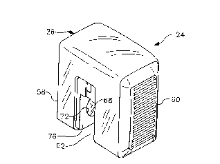
first and second end ~ections 58 and 60 with a rectan-
gularly configured gap 62 therebetween. With the
transducer assembled to airway adapter 22, the two
sections 58 and 60 of transducer casing 26 embrace
those two inner side walls 64 and 66 of airway adapter
central section 34 in which energy transmitting
windows 52 and 54 are installed.
optically transparent windows 68 and 70 are
installed along optical path 50 in apertures 72 and 74
provided in the inner end walls 76 and 78 of transduc-
er housing 26. These windows allow the beam of
infrared radiation generated in unit 28 in the left-
hand end section 58 of transducer housing 26 to pass
to airway adapter 22 and from the airway adapter to
the detector unit 30 in the right-hand section 60 of
the transducer housing. At the same time, windows 68
and 70 keep foreign material from penetrating to the
interior of the transducer casing.
Referring now to FIGS. 3-10, the unit 28
employed to emit infrared radiation, to form that
energy into a beam, and to propagate the beam along
optical path 50 includes: an infrared radiation
emitter 80, a commutator 82, a tube or cap 84, and a
mirror component 86, all supported from a base 88.
Infrared emitter or energy source 80, best
shown in FIGS. 5 and 6, is of a unique thick film
W O 91/18279 PCT/~'S91/03598
2083509
construction. It includes a substrate 90 which, in
one actual embodiment of the invention, is 0.250 inch
long, 0.040 inch wide, and 0.005 inch thick. This
substrate can however range in thickness from 0.003 to
0.005 in., and it is formed from a material having low
thermal conductivity. Steatite (a polycrystalline
material containing magnesium oxide and silicon
dioxide) is preferred because it has a thermal conduc-
tivity which is on the order of one magnitude less
than conventional low thermal conductivity materials
such as alumina. This i~ important because it sig-
nificantly reduces the power required to heat the
emitter to its operating temperature.
However, alumina can be employed instead of
steatite. It if is, the substrate is preferably
coated with a film of a dielectric material having low
thermal conductivity such as a dielectric glass.
Another substrate material that can be employed
is fused silica.
Bonded to the upper surface 92 of substrate 90
are two T-shaped electrical conductors or terminals 94
and 96. In the exemplary infrared radiation emit-
ter 80 illustrated in FIGS. 5 and 6, the head 98 of
each conductor is .035 inch long; and the gap 100
between the conductors is 0.030 inch.
Terminals 94 and 96 are preferably formed of a
platinum and gold containing cermet obtained by
printing an ink such as DuPont's 4956 on the sur-
face 92 of substrate 90 and then firing the substrate.
Superimposed on terminals 94 and 96 and bonded
to the upper surface 92 of substrate 90 with its ends
overlapping conductors 94 and 96 is a thick film or
layer 102 of an emissive, electrically resistive
WO91/18279 PCT/US91/03598
2083509
33
material. The preferred material i~ obtained by
firing Electro-Science Labs ES~3812 Ink. This ink
contains a major proportion of platinum and has an
operating temperature in the range of 250-300 degrees
centigrade.
The illustrated, exemplary, emissive layer 102
is 0.070 inch long; and the two ends 104 and 106 of
the emitter overlap 0.020 inch onto the conductor 94
and the conductor 96 of emitter 80. Thus, the total
overlap constitutes 57 percent of the total area of
emissive layer 102. This is within the preferred and
operable range of 50 to 60 percent.
Overlaps in the range just described tend to
keep the current density at the interfaces between
emissive layer 102 and conductors 94 and 96 from
becoming too high and causing emitter 80 to fail by
burnthrough or fatigue cracking of the emissive layer.
That we can thus prevent failures of emitter 80
is surprising. Heretofore, it has been believed that
successful performan~e of a thick film device with an
active layer-to-conductor overlap could not be ob-
tained with an overlap P~ee~ing about 15 percent.
Also contributing to the resistance to failure
from exposure to excessive current densities is the
T-shaped configuration of conductors 94 and 96. This
is at least potentially superior to the more conven-
tional rectangular or straight sided conductors as far
as resistance to emissive layer burnthrough is con-
cerned.
It is one of the important features of the
present invention that the emissive layer 102 and
substrate 9o of emitter 80 are so constructed and
related as to optimize the performance of the emitter
WO91/18279 PCT/US91/03598
20835 D 9
34
as the emissive layer is periodically heated to
produce the wanted emission of radiant energy. This
important result is obtained by ~o correlating the
dimensions and thermal conductivities of the emissive
S layer and substrate with the duty cycle of power
supply as to satisfy the equation:
PP{ R~I [d~ d)(l -e ttr~ R~ [d+(l -d)(l -e t/rl~)]~
T(t)= ~ T"~[d+(l d)(l~e%n~)] 3+ro foro5t<td~
Pp{RTI [d~(l -d)(l -e t i/T13e~td/~]+RT~ [d~(l -d)(l -e ti/~c)e-td~/~+
RTm [d~(l -d)(1 -e t ;/TI )e td/~I]}+ TO. for td<ts tp
For td < t ~ tp wh ere t j = t-td
where:
I, II, and III are, respectively: the omissive
layer of the emitter, II is that part of the substrate
layer covered by the emissive layer, and III is the
sum of the remaining, end sections of the substrate
layer.
A = cross sectional area perpendicular to the
major heat flow;
L = thickness of a layer parallel to the
direction of major heat flow;
p = (rho) density of the layer material;
c = specific heat of the layer material;
WO 91/18279 PCl/lJS91/03598
2083~09
k = thermal conductivity of the layer materi-
al;
RT = 'Thermal Resi~tance' of the layer, where
RTI' RTII and RTIII for lay-
ers I, II and III respectively;
CT = 'Thermal Capacitance' of the layer;
IT = 'Thermal Current' or heat flow;
VT = ~Thermal Voltage~ or temperature;
r = 'Thermal Time Constant' of the layer,
where ~ = RTCT for each layer I, II and
III.
Heat flow equation: VT(t) - RTIT(t) exp(-t/~);
To = ambient temperature of the back surface
of the layer;
15 T(x) = temperature as a function of location in
the layer, (O S X S L);
pp = peak electrical power applied to the
thick film resistor;
Pave average electrical power applied to the
thick film resistor;
g(t) = general on-off pulsing function;
td = time the pulse voltage is ON;
tp = period of the pulsing wave form;
t; = T-T~ when t~ ~t<tp;
25 d = duty cycle of the pulsing waveform, where
d = td/tp.
In the.model VT(t) = RTIT(t) exp(-t/r) is replaced by
~(x,t~ = RT[Pave+(Pp~Pave)~(t)¦= PpRT~d + (1-d)g(t)~,
x=0
As will be apparent to the reader from the
foregoing model, the following are the critical
WO91/18279 PCT/~'S91/03598
2083~09
parameters of an emitter of the character disclosed
herein:
Emissive Element Density p
Specific Heat C
Thermal Conductivity k
Thickness L
Substrate Density p
Specific Heat C
Thermal Conductivity k
Thickness L
The thermal model also makes it clear that the
various parameters of the emi~sive element, as well as
those of the substrate, have to be balanced to obtain
an emitter that will emit infrared energy of predic-
table varying intensity. This variation is controlled
by the voltage across the source.
The majority of the energy generated by the
dissipation of the power through t~e resistor is
conducted away from the resistor through that com-
ponent and the substrate of the emitter in the form of
thermal energy or heat. The rate at which this heat
is conducted away from the emissive element or resis-
tor is controlled by the physical parameters of the
resistor, conductor, substrate and mounting as-
semblies.
Also important to the performance of the
emitter is the emissivity of the resistor surface. It
does no good to modulate the heat of the resistor
surface if that resistor surface is inefficient in
radiating the concomitant infrared energy.
The emissivity and resulting emission of
infrared energy (heat) from the resistor is negligible
WO91/18279 PCT/US91/03~98
2083509
in terms of the total heat flow of the system, but it
is quite important in the functioning of the resistor
assembly as an efficient infrared radiation emitter.
Thus, the total assembly of emitter components
must be considered when modeling the heat flow since
the resistor and conductor , as well as the substrate
material, are all within one order of magnitude for
all parameters. Consequently, changes in the thick-
nesses, when all other parameters are held constant,
will significantly affect the temperature excursions.
These effects are seen both analytically and ex-
perimentally.
Nevertheless, changing the substrate thickness
from .003" to .005" with correlated changes in other
emitter components did not unacceptably affect the
thermal performance of the emitter. This is sig-
nificant in that the thicker substrate makes a more
rugged emitter which is less susceptible to breakage.
It has of course been found, as predicted by
the thermal model, that the emissive element thickness
for a given resistance must be tightly controlled to
obtain satisfactory performance. This is because the
thermal conductivity of the emissive layer is much
higher than that of the substrate. S nce the emissive
layer thickness is only about one-fourth to one-fifth
that of the substrate, small variations in the emis-
sive element thickness have large effects on the
thermal performance.
One important item that can be determined from
the model is the wave shape of the emitted infrared
radiation for a defined set of physical parameters.
This is important because of the time and other
savings that can be realized by not having to build
WO91/18279 PCT/US91/03598
2~83509
38
and evaluate large numbers of prototypes. That is,
the performance of an emitter is tied directly to the
wave shape of the emitted energy. Consequently, one
can use the thermal model to evaluate different sets
5 of selected parameters without actually building and
testing emitters with those parameters.
Other important items of information can also
be readily derived from the thermal model. As an
example, one gas analyzer system with an infrared
radiation emitter of the character defined by the
thermal model requires at least a 16 volt drive at 48
Hz with a 10% duty cycle to provide sufficient emitter
output for the system to function to specification.
If the substrate material of the emitter were to be
changed from steatite to alumina, the voltage would
have to be increased to over 21 volts to obtain
comparable performànce. However, at this higher
voltage, the resistor material breaks down due to
overheating. Thermal effects such as these can be
modeled and materials chosen that will allow for as
high a peak temperature with as much modulation of the
temperature and as low a dissipated power as possible
Other criteria that are important in designing
an infrared emitter of the character disclosed herein
are the frequency and duty cycle of the electrical
power source employed to drive the emitter. By using
the thermal model to compare the differences between
two different emitter outputs from similar resistors
driven with different pulse streams, one can more
easily determine optimum driving conditions.
Previously proposed mathematical models for
infrared radiation sources which fail to take the
electrically resistive, emissive layer into account,
Wogl/18279 PCT/US9l/03598
2083509
such as that disclosed in U.S. patent No. 4,620,104
issued 28 October 1986 to Nordal, are woefully inade-
quate. The emissive layer will typically comprise 25
percent of the thickness of the infrared radiation
emitter. The effect of that component can therefore
not be neglected, as heretofore been done, with any
expectation that a mathematical model will accurately
reflect the actual operation of the infrared radiation
source.
Referring now more specifically to FIGS. 3-6,
commutator 82 is stamped from a sheet of conductive
metal such as tin plated copper. The emitter has two,
generally similar, arcuate segments 108 and 110
connected by integral tabs 112 and 114, a conductor or
terminal 116 integral with and extending radially from
segment 108, and a second conductor or terminal 118
which is integral with and extends radially from
commutator segment 110 in the opposite direction at a
location halfway around the circumference of the
commutator from terminal 116.
As just indicated, each of the two commutator
segments 108 and 110 has a generally arcuate con-
figuration. U-shaped alignment ~lots 120 and 122 open
onto the periphery of segment 108, and a third,
U-shaped alignment slot 124 opens onto the periphery
of segment 110. Also opening onto the peripheries of
commutator segments 108 and 110, respectively, are
conductor receiving slots 126 and 128.
Additionally found in commutator 82 are emitter
supports 130 and 132. Support 130 is integral with,
and extends radially inward from, commutator seg-
ment 108. Emitter support 132 is axially aligned with
support 130. It is integral with, and extends radial-
.
WO 91/18279 PCI/l'S91/03598
20835~9
ly inward from, commutator 5egment 108. Emittersupport 130 has an emitter receiving recess 134 on
what will hereinafter be referred to as the bottom
side 136 of commutator 82; and a second emitter
S receiving recess 138 is formed in emitter support 132,
also on the bottom side 136 of commutator 82.
One end 140 of emitter 80 is seated in emitter
support recess 134 and bonded in place as by the
illustrated epoxy adhesive 142, and the opposite end
143 of the emitter is left free to float. By way of
surface tension, the epoxy adhesive draws emitter 80
into the position illustrated in FIG. 5. This locates
the midpoint 144 of emitter 102 on the centerline 145
of emitter unit 28. This is important in that it op-
timizes the ability of mirror assembly 86 to collateand focus the energy emitted from the thick film or
layer 102; and this results in an optical beam of
optimum quality being projected from emitter unit 28.
In particular, and as shown in FIG. 5,
there is an elongated, transversely oriented slot 146
in commutator segment 108 at the left-hand end of
emitter receiving groove or recess 138. Because of
slot 146, the epoxy adhesive 142 will not flow past
the boundary identified by reference character 147 in
FIG. 5. Consequently, the left-hand, fixed end 140 of
emitter 82 is drawn even with, but not beyond, bound-
ary 147. With end 140 of the emitter so located, the
emitter is precisely centered on the longitudinal
centerline 145 of unit 28.
The opposite end 143 of the emitter is seated
in the slot 138 in emitter support 132. However, that
end of emitter 80 is not bonded to that support but
is, instead, free to move back and forth in the slot
. --
W O 91/18279 PC~r/US91/03598
2~83509
as indicated by arrow 148 in FIGS. 5 and 6. As a
consequence, when current is supplied across the
emissive layer 102 of emitter 80, heating up the
emissive layer and substrate 90, the substrate grows
or increases in length due to thermal expansion; but
-this growth is accommodated rather than being con-
~ strained. As a consequence, the ~tresses which would
be imposed upon emitter 80 if both ends were fixed are
avoided, eliminating the damage to emitter 80 or
complete failure of that component which might result
if mechanical stresses were imposed upon it.
After emitter 80 has been assembled to com-
mutator 82, the two termin~l~ 94 and 96 are respec-
tively connected to conductive segments 108 and 110 of
the commutator 82. Electrical conductors or leads
soldered at opposite ends to the emitter unit ter-
minals 94 and 96 and commutator segments 108 and 110
are employed for this purpose. They are illustrated
in ~IG. 5 and identified by reference characters 149
and 150.
Once the steps just discussed have been com-
pleted, commutator terminals 116 and 118 are bent at
right angles to the conductor segments 108 and 110 of
the commutator, and the emitter or commutator assembly
is then installed in the base 88 of radiant energy
emitting unit 28. This component, best shown in
FIGS. 3 and 4, is a monolithic member. The environ-
ment in which this component operates can reach an
elevated temperature due to heating by the emissive
layer 102 of emitter 80. The base is therefore
fabricated of a polysulfone or comparable polymer
which will remain structurally stable at the tempera-
tures it reaches during the operation of emitter
Wogl/18279 PCT/US9l/03598
2083509
unit 28 and as leads 149 and 150 are soldered to base-
supported commutator segments 108 and 110.
Base 88 has a cylindrical configuration; a
platform 151; and integral, annular wall seg-
5 ments 152158 which extend upwardly from plat-
form 151 with base 88 in the orientation shown in
FIG. 4. Extending inwardly from each of wall seg-
ments 152, 154, and 158 is a boss 160, 162, or 164
configured to complement a corresponding one of the
three U-shaped slots 120, 122, and 124 in the seg-
ments 108 and 110 of commutator 82. Diametrically
opposed slots 166 and 168 are formed in, and extend
from the top to the bottom of, base 88. These slots
open onto the exterior of the base, are slightly wider
than the terminals 116 and 118 of commutator 82, and
are slightly deeper than the commutator terminals.
Consequently, the terminals 116 and 118 may be fitted
within slots 166 and 168 when emitter unit 28 is
assembled.
The assembly of emitter 80 and commutator 82 is
installed in base 88 by aligning it relative to the
base as shown in FIG. 4 and then displacing the
emitter/commutator assembly downwardly in the direc-
tion indicated by arrow 170 until the segments 108
and 110 of the commutator are seated on the upper
surface 172 of base platform 151.
The radial bosses 160...164 of base 88 guide
commutator 82 relative to base 88 as the com-
mutator/emitter assembly is installed, then and
thereafter maintaining the wanted relationship between
the assembly and base. Once commutator segments 108
and 110 are seated on the platform 151 of base 88, the
emitter/commutator assembly is retained in place by an
W O 91/18279 P ~ /US91/03598
2083509
appropriate adhesive (not ~hown) between the com-
mutator segments and the upper surface 172 of the
platform.
As is apparent from FIGS. 3 and 4, there is an
asymmetrical relationship of the radially oriented
lugs or bosses 160...164 on base 88 and the complemen-
tary notches 120...124 of commutator 82. This is an
important feature of the present invention, as far as
the just-dis~lc~-~ installation of the emit-
ter/commutator assembly is concerned, because it keeps
the commutator from being installed upside down in
base 88.
After the emitter/commutator assembly is
installed and bonded to base 88, the two commutator
tabs 112 and 114 are removed, leaving gaps 174 and 176
between the commutator segments 108 and 110. This
electrically isolates commutator segment 108 from
segment 110. Therefore, current supplied to one of
the commutator terminal~ 116 and 118 flows from the
associated commutator segment 108 or 110 through
emitter 80 and the second commutator segment to the
second of the two commutator terminals. For example,
current applied to terminal 116 flows seriatim
through: commutator segment 108, lead 149, emitter
terminal 94, emissive layer 102, emitter terminal 96,
lead lS0, and commutator segment 110 to commutator
terminal 96. This results in emissive layer 102 being
heated and emitting the wanted energy in the infrared
portion of the electromagnetic spectrum.
The provision of the breakaway tabs 112 and 114
just discussed is an important feature of the present
invention from the viewpoint of assembling emitter
unit 28. The assembly of emitter 80 and commutator 82
WO 91/18279 PCr/~'S91/03598
2083S09
i~ quite fragile as are the connections from leads 149and 150 to emitter terminals 94 and 96 and commutator
segments 108 and 110. The assembly would be difficult
to handle, install, and align if commutator seg-
ments 108 and 110 were separate components. Withcommutator segments 108 and 110 integrated, however,
this ceases to be a problem because the commutator
acts as a supporting frame as well as an assembly jig.
Handling and installation are very much simplified,
especially as the removal of tabs 112 and 114 subse-
quent to the installation of the emitter/commutator
assembly is easily accomplished.
From another viewpoint, an emitter/commutator
assembly with separate commutator segments would
require a special and relatively difficult to use
fixture to install; and, even then, handling of this
fragile assembly would pose a problem. In contrast,
by employing the unitary commutator with its breakaway
tabs, the commutator can be made to serve as an
integral, assembly fixture for the emitter and com-
mutator.
Once the emitter/commutator assembly has been
installed in and bonded to base 88 and tabs 112
and 114 removed, emitter unit tube or cap 84 is
installed. This component, shown in FIGS. 3 and 8-10,
is an annular member fabricated from a polymer with a
high degree of structural stability such as acrylo-
nitrile-butadiene-styrene (ABS).
Cap 84 is of the same diameter as base 88. It
has a flat platform 178 from which a circular array of
annular bosses 180...188 separated by gaps 190...197
depend.
W O 91/18279 PC~r/US91/03598
2û83509
Cap 84 is installed by displacing it relative
to base 88 in the direction indicated by arrow 198 in
FIG. 3, once the cap has been oriented relative to the
base as shown in that f igure. As this movement
continues, the annular wall segments 152...158 of
base 88 ride up through the slots or gaps 190...197 in
cap 84 until the platform 178 of the cap is seated on
the upper ends of the annular walls segments.
An appropriate, but unillustrated, adhesive is
employed to secure cap 84 to base 88.
With cap 84 installed, the gaps 190 and 194
between depending, annular segments 152, 154, and 158,
160 are aligned with the external slots or reces-
ses 126 and 128 in base 88. This accommodates the two
terminals 116 and 118 of commutator 82 in cap 84.
The remaining step in putting together emitter
unit 28 is to install mirror component or assembly 86
in base 88.
The mirror assembly, best shown in FIGS. 3, 7,
9, and 10, is a monolithic member with a circular
cross section. The mirror assembly, also typically
fabricated from ABS, is dimensioned to fit within the
circular central bore 200 of emitter base 88. A
circular recess 202 is formed in mirror assembly 86,
and that recess opens onto the bottom side 204 of the
mirror assembly. A second, parabolic surface 206 is
formed in the opposite, upper side 208 of the assemb-
ly. Parabolic surface 206 is first plated with a
typically 2 mil thick coating of copper and then over-
plated with gold, the thickness of the gold layertypically being in the range of 2 ~in. This provides
a parabolic mirror for collating and focusing the
infrared radiation from emitter 80.
Wo 9l/18279 PCr/US9l/03~98
2083S~3
46
As is best shown in FIG. 3, the upper part 210
of mirror assembly 86 is stepped inwardly, leaving a
pair of longitudinally extending, diametrically
opposed lugs 212 and 214. The upper part 210 of the
5 mirror assembly is cut away, leaving diametrically
opposed, longitudinally extenAirg grooves 216 and 218
with locations 90~ removed from those of lugs 212 and
214.
Mirror assembly 86 is installed in base 88 with
10 its axis of symmetry coinciding with emitter unit
longitudinal centerline 145. This is accomplished by
moving the mirror assembly relative to the base as
indicated by arrow 220 in FIG. 3. As this displace-
ment continues, the just-described lugs and
grooves 212... 218 interact with corresponding, in-
tegral, longitudinally extending lugs 222 (only one of
which is shown) and grooves 224 in base 88 to guide
the mirror assembly relative to the base. As in the
case of cap 84, an appropriate but not illustrated
20 adhesive can be employed to hold the mirror assembly
in place.
As shown in FIG. 10, there is a notch 226 in
the upper end of mirror component 86. This separates
upper side 208 of emitter 80 from the mirror com-
25 ponent 86, eliminating the possibility of damage tothe emitter or to the mirror-providing plating on the
parabolic surface 206 of the mirror component.
Referring again to the drawing, FIGS. 11-17
depict a second infrared radiation source or emitter
30 unit 338 also constructed in accord with, and embody-
ing, the principles of the present invention.
The major components of emitter unit 338 are:
(1) a base 340, (2) a commutator 342, (3) an infrared
-
W091/18279 PCT/US9l/03598
2083509
radiation emitter or source 344, (4) conductive
leads 346 and 348 for connecting emitter 344 across an
appropriate power source, and (5) a mirror assemb-
ly 350 for collating and projecting from unit 338 in
the form of a beam infrared radiation outputted by
emitter 344.
Emitter 344 may be a duplicate of the emit-
ter 80 discussed above.
The base 340 of emitter unit 338 is a generally
cylindrical component with a central aperture 352
through which the beam of infrared radiation formed
and projected by mirror assembly 350 can escape to the
exterior of unit 338. Like its complement in emitter
unit 28, base 340 is preferably fabricated from a
polysulfone or other polymer resistant to high temper-
atures.
With emitter unit 338 in the orientation shown
in FIGS. 11, 12, and 15, base 340 has a vertically
oriented, circular side wall 354; an internal,
horizontal ledge 356 surrounded by side wall 354; and
diametrically opposed locator lugs 358 and 360.
As is best shown in FIGS. 15 and 16, the
commutator 342 employed in unit 338 is made up of two
identical, arcuate segments 362 and 364. Like their
counterparts in unit 28, they may be fabricated from
tin plated copper. From the practical viewpoint, this
employment of identical commutator segments is impor-
tant in that it reduces the number of parts that must
be stocked. Commutator segments 362 and 364 are also
simpler and therefore considerably cheaper to fabri-
cate than the more complicated, integrated com-
mutator 82 employed in emitter unit 28.
-
WO9l/18279 PCT/US9l/03598
20~33509
48
Each of the commutator segments 362 and 364 has
an integral, inwardly extending, emitter support 366
with an emitter receiving groove 368. The groove
opens onto the bottom sides 370 of the commutator
segments 362 and 364 and extends to the free ends 372
of emitter supports 366.
Formed in each of the emitter supports 366
adjacent its emitter receiving rer~ or groove 368 is
an elongated, radially exten~i~q slot 374. With the
commutator segments 362 and 364 installed in base 340
and seated on the ledge 356 of that base as shown in
FIG. 14, the locator lugs 358 and 360 of base 340
extend through the slots 374 in emitter supports 366.
That locates commutator segment5 362 and 364 relative
to base 340.
Also employed to locate commutator segments 362
and 364 in the base 340 of emitter unit 338 are
cooperating pairs of dep~Aing, integral lugs 376
and 378. These are found at the ends of each com-
mutator segment's emitter ~u~rt 366. With thecommutator segments assembled to emitter base 340 as
shown in FIGS. 13-15, lugs 376 and 378 fit into
complementary notches 380 and 382. These notches are
located on opposite sides, and at the free ends 372,
of the emitter supports. The sides of the notches
thereby embrace the opposite sides of the supports 366
to hold in place the commutator segments 362 and 36
in which those supports are incorporated.
once installed, commutator segments 362 and 364
are bonded in place and to emitter base 340 by an
appropriate adhesive applied at the locations indi-
cated by reference character 384 in FIG. 15. With the
two commutator segments 362 and 364 installed in
WO 91/18279 PCI/VS91/03598
2083509
49
emitter 344 in the manner just described, they are
electrically isolated by the gaps 386 and 388 between
the segments.
After commutator segment~ 362 and 364 have been
installed in base 338, emitter 344 is added to the
assembly. It is seated in those emitter-receiving
grooves 368 located in the commutator segment-provided
emitter supports 366 with the emissive layer 389 of
the emitter centered on the longit~l~inAl center-
lo line 390 of unit 338 and spanning the gap 392 betweenthe ends of emitter supports 366.
End 394 of emitter 344 is bonded to its sup-
port 366. But, as in emitter unit 28, the opposite
end 396 of the emitter is not. This leaves emit-
ter 344 free to grow or eY~An~ longitudinally as itheats up during operation; and this keeps from there
being imposed on the emitter stresses which might
damage or destroy it.
Emitter 344 is electrically connected to
commutator segments 362 and 364 after it is installed
by electrical leads 398 and 400. At one end, lead 398
is soldered to commutator segment 362. The other end
of the lead is soldered to the terminal 94 at the
fixed end 394 of the emitter. Lead 400 is similarly
soldered at opposite ends to commutator segment 364
and the terminal 96 at the opposite, floating end 396
of emitter 80.
External leads 346 and 348 extend upwardly
along the inside of base side wall 354 and into
diametrically opposed, semicircular recess 402 and 404
in the rims of commutator segments 362 and 364. Here,
they are soldered to the commutator segments.
WOgl/18279 PCT/US9~/03598
208~09
so
With the electrical connections just described
completed, current supplied from the external source
flows from external lead 346 through commutator
segment 362, lead 398, emitter terminal 94, the
electrically resistive, emissive layer 389 of the
emitter, emitter terminal 96, lead 400, and commutator
segment 364 to external lead 348 or through the same
set of components but in the opposite direction. In
both cases, the current flowing through emissive
layer 389 causes the latter to heat up and output the
wanted infrared radiation.
The final, and typically last to be installed,
major component of emitter unit 338 is mirror com-
ponent 350.
This component, shown in FIGS. 11, 12, 15,
and 17, has a circular cross-section of the same
diameter as base 340. It is typically fabricated from
ABS polymer or a polymer with comparable characteris-
tics.
Grooves extending from end-to-end of mirror
component 350 accommodate the external leads 346
and 348 of emitter unit 338. One of these grooves is
shown in FIG. 15 and identified by reference charac-
ter 406.
The upper surface 408 of mirror component 350
has a parabolic configuration. Surface 408 is plated
first with copper and then with gold to provide a
mirror for collating the energy from emitter 344 and
then focusing that infrared radiation into a beam
projected from the emitter unit.
A groove 410 extends around the periphery of
mirror component 350. With the mirror component
assembled to the base 340 of emitter unit 338, the
WO 91/18279 PCI/US91/03598
2083509
51
side wall 354 of the base surrounds the upper part 412
of mirror component 350. ThiE; protects mirrored
surface 408 from damage.
The lower end 414 of groove 410 also provides
a seat for base 340. This keeps emitter 344 from
engaging and perhaps being damaged by base 340.
Generation of a detector output signal of a
high enough signal-to-noise ratio to be useful re-
quires that the beam of attenuated infrared radiation
falling on the detector of a NDIR transducer as
disclosed herein and identified by reference character
24 be modulated. It was pointed out above that this
can be done by applying bipolar electrical pulses to
the electrically resistive, emissive component of a
thick film infrared radiation ~ource such as those
disclosed above and identified by reference characters
28 and 338.
The power supply 33 employed to drive the
emitter 80 of infrared source unit 28, shown in block
diagram form in FIG. 18, outputs pulses of this
character. It includes an H-bridge driver cir-
cuit 302, timing circuits collectively identified by
reference character 304, pulse width and frequency
watchdog circuits 306 and 308, a power on reset
circuit 310, and a power supply watchdog circuit 312.
The load, emitter 80 of infrared source unit
28, is connected across the outputs of H-bridge driver
circuit 302. These outputs are identified as SOURCE+
and SOURCE- in FIG. 18.
Circuits 304 supply timing signals to driver
302. The timing signals are derived from a crystal
oscillator (not shown) and then counted down to
provide the desired pulse rate and duty cycle. A
WO 91/18279 PCI/US91/03598
Z083509
52
current implementation uses a 7 megahertz oscillator
to provide an 85 . 45 Hz pulse rate at a 7.1% duty cycle
(this value is the part of the duty cycle in which
both one positive signal and one negative signal are
outputted). The timing circuits are not, by themsel-
ves, part of the present invention. Accordingly, they
will be described herein only to the extent necessary
for an unders~An~ing of the present invention.
Timing circuits 304 provide three signals to
driver circuit 302: (1) PHASE 1 (0~), a series of
pulses basically corresponding to the time during
which the driver circuit generates the positive output
signal SOURCE+; (2) PHASE 2 (02), a series of pulses
basically corresponding to the time period during
which the driver circuit generates the negative output
signal SOURCE-; and (3) ENABLE (E), a signal that must
be present for the driver circuit to generate the
positive and negative source voltages SOURCE+ and
SOURCE-.
Positive input voltage +Vp and negative input
voltage-Vp signals are also supplied to driver cir-
cuit 302. Based on the PHASE 1 (0l) PHASE 2 (02) and
ENABLE (E) signals provided by the timing circuits,
the driver circuit 302 generates bipolar outputs
SOURCE+ and SOURCE-, which are derived from the input
voltage signals +Vp and -Vp.
The signals PHASE 1 (0l) and PHASE 2 (02) are
also supplied to pulse width watchdog circuit 306 and
frequency watchdog circuit 308. The pulse width
watchdog circuit 306 measures the width of each pulse
of both the PHASE 1 (0l) and the PHASE 2 (02) signals.
If the width of any pulse of either the PHASE 1 (0l) or
the PHASE 2 (02) signals exceeds a predetermined value,
WO91/18279 PCr/US91/0359X
2083509
the pulse width watchdog circuit 306 forces the
ENABLE (E) signal LOW, thereby preventing the driver
circuit 302 from generating an output voltage.
The frequency watchdog circuit 308 determines
s whether the frequency of either the PHASE 1 (0l) or the
PHASE 2 (02) signals ex~eedc a predetermined value or
whether extra pulses are generated. If either of
these conditions exist, the frequency watchdog cir-
cuit 308 shuts off the ~N~Rr~ (E) signal, thereby
preventing the driver circuit from generating an
output voltage.
Power supply watchdog circuit 312 monitors the
input voltages +Vp and -Vp of the signals supplied to
driver circuit 302. The power supply watchdog cir-
cuit 312 shuts off the ENABLE (E) signal, preventing
the driver circuit 302 from generating an output
voltage, if the positive input voltage ~Vp falls below
a positive threshold value ~V~ or the negative input
voltage -Vp exceeds a negative threshold value -V~.
When any of the watchdog circuits determines
that a fault condition requiring the shutdown of the
driver circuit 302 exists, the appropriate watchdog
circuit forces the ENABLE (E) signal LOW, thereby
shutting off the driver circuit 302 for as long as the
fault exists. When the fault condition clears, the
appropriate watchdog circuit no longer suppresses the
ENABLE (E) signal. However, the power-on reset
circuit 310 delays reinstatement of the ENABLE (E)
signal to a HIGH condition to allow the timing cir-
cuits and other circuitry to become stable before the
driver circuit 302 begins generating source voltages.
As shown in FIGS. l9B and l9C, driver cir-
cuit 302 contains power MOSFETs 314, 316, 318, and 320
WO 91/18279 PCr/US91/03598
2083509
arranged in an H-bridge configuration. MOSFET drive
circuits 322, 324, 326, and 328 control MOSFETs 314,
316, 318, and 320, respectively.
MOSFET drive circuit 322 consists of AND gate
330, turn-on delay circuit 332, inverter 334, and a
MOSFET 336. Turn-on delay circuit 332 comprises
parallel RC circuit 338 and NAND gate 340.
MOSFET drive circuit 324 consists of AND
gate 342, turn-on delay circuit 344, inverter 346, and
MOSFET 348. Turn-on delay circuit 344 includes
parallel RC circuit 350 and NAND gate 352.
MOSFETS 336 and 348 are for translating the
outputs of inverters 334 and 346 into signals ap-
propriate for controlling MOSFETS 314 and 316, respec-
1~ tively.
MOSFET drive circuit 326 includes turn-on delay
circuit 3s6 and inverter 358. Turn-on delay cir-
cuit 356 includes a parallel RC circuit 360 and NAND
gate 362.
MOSFET drive circuit 328 includes a turn-on
delay circuit 364 and inverter 366. Turn-on delay
circuit 364 consists of parallel RC circuit 368 and
NAND gate 370.
Signals ENABLE, PHASE 1 (0l)~ and PHASE 2 (02)
and all voltages for powering drive circuit 302 are
externally provided. The ENABLE signal enters the
circuit through transistor 372, while the PHASE 1 (0~)
signal enters through transistor 374.
Signals ENABLE (E) and the inverse of the
PHASE 1 (0~) signal, which is generated by inverter 376
and identified as ~HA~ 1 (0~J are applied to the
inputs of AND gate 330. The ENABLE signal and the
PHASE 1 (0~) signal are applied to the inputs of AND
WO 91/18279 PCI/US91/0359X
2083509
gate 342. Thus, pulses cannot be outputted by driver
circuit 302 unless the ENABLE (E) signal i5 HIGH. The
PHASE 1 (0l) signal and its inverse ~A~ J are
also applied to turn-on delay circuits 356 and 364,
respectively.
As discussed above, turn-on delay circuit 332
includes~RC circuit 338 and NAND gate 340. The output
of AND gate 330 is sent directly to one input terminal
of NAND gate 340 and to the other input terminal via
RC circuit 338. Since RC circuit 338 delays the rise
of the output of AND gate 330, NAND gate 340 goes HIGH
a short period T~ after AND gate 330.
Turn-on delay circuit 332 thus delays slightly
the changing of the output of AND gate 330 from an OFF
state to an ON state. The change of the output of
AND gate 330 from an ON state to an OFF state is
basically unaffected by L~l, on delay circuit 332.
Inverter 334 renders the polarity of the output
from NAND gate 340 appropriate for driving MOSFET 336
to turn on MOSFET 314.
MOSFET drive circuit 324 operates in the same
manner as MOSFET drive circuit 322 and will not be
discussed in detail. It is sufficient in this respect
to point out that, as the PHASE 1 (0~) signal is
directly applied to the input of its AND gate 342,
MOSFET drive circuit 324 turns on MOSFET 316 only when
MOSFET 314 is turned off.
MOSFET drive circuits 326 and 328 operate in
basically the same manner as MOSFET drive circuits 322
and 324, differing only in the following respects.
First, because the sources of MOSFETs 320 and 318 are
connected to a negative potential, inverters 358
and 366 of circuits 326 and 328 directly drive MOS-
W O 91/18279 PC~r/~'S91tO3598
2083509
FET6 318 and 320, respectively, without a translatingdevice such as the MOSFET~ 336 and 348 used in MOSFET
drive circuits 322 and 324. Second, AND gates corre-
sponding to AND gates 330 and 342 in MOSFET drive
circuits 322 and 324 are not used in MOSFET drive
circuit~ 326 and 328. These AND gates are omitted
because turning off MOSFETS 314 and 316 with the
ENABLE (E) signal is sufficient to turn off the entire
drive circuit 302.
As will be apparent to the reader from the
foregoing, MOSFET drive circuits 322, 324, 326,
and 328: (a) turn on MOSFETs 316 and 318 and turn off
MOSFETs 314 and 320, thus supplying the SOURCE- signal
during a PHASE 2 (02) pulse; (b) turn on MOSFETs 314
and 320 and turn off MOSFETs 316 and 318, consequently
supplying the SOURCE~ ~ignal during a PHASE 1 (0~)
pulse; and (c) turn off MOSFETs 314 and 316 whenever
the ENABLE (E) signal goes LOW.
MOSFETs 314 and 316 are connected to a positive
potential of +12V. The posi~ive potential is provided
by regulating circuit 378, which is composed of
voltage regulator 380 and a variable resistor 382 for
adjusting the voltage output of voltage regulator 380.
A device such as an LM317 IC chip and its associated
circuitry may be used as voltage regulator 380.
Positive input voltage +Vp is applied to the input
terminal of voltage regulator 380, and the regulated
output of voltage regulator 380 is supplied to MOS-
FETs 314 and 316.
Similarly, MOSFETs 318 and 320 are connected to
a negative potential of -12V in this embodiment, as
shown in FIG. l9C. The negative potential is provided
by regulating circuit 384. Regulating circuit 384
WO 91/18279 PCI/US91/03598
2083509
consists of voltage regulator 386. A device such as an
79M12 IC chip and its associated circuitry may be used
as the voltage regulator 386. Negative input vol-
tage -Vp is applied to an input terminal of voltage
regulator 386, and the output of voltage regulator 386
is connected to the 80U~ of MOSFETe 318 and 320.
The voltage applied to~MOSFETe 318 and 320 is thereby
kept stable.
Driver circuit 302 also includes a differential
amplifying circuit 388, a resistor 392, and a peak
hold circuit 394. Differential amplifying circuit 388
comprises a differential amplifier 390. An OPO7 IC
chip and its associated circuitry may be used as
differential amplifier 390. Resistor 392 is a 1 ohm
resistor in series with the load (emitter 80) of the
SOURCE- output voltage.
The differential amplifier 390 measures the
current through resistor 392 and outputs a voltage
signal corresponding to the current through resis-
tor 392. Peak hold circuit 394, which may be based onan LF398 IC chip or similar circuitry, measures and
holds the maximum voltage output of differential
amplifier 390. The peak value of the output of
differential amplifier 390 reflects the peak current
generated by drive circuit 302 and may accordingly be
monitored to determine whether the drive circuit 302
is functioning properly.
The pulse width watchdog circuit 306 (FIG. l9A)
includes comparators 400, 402, 404, and 406. RC cir-
cuits 408 and 410 are connected to the outputs of com-
parators 400 and 404, respectively. Comparator 400
and its associated circuitry are so designed that the
output of comparator 400 is HIGH when the PHASE 1 (0l)
WO91J18279 ~CT/US9l/03598
2083~09
58
signal i5 HIGH and LOW when the PHASE 1 (0~) signal i6
LOW. RC circuit 408 delays the rise of the output
voltage of comparator 400 for a time interval T~
predetermined by the values of the resistor and
capacitor in RC circuit 408. Comparator 402 compares
the delayed output of comparator 400 with a reference
voltage. If the delayed ou~ of comparator 400
exceeds the reference level at the input of com-
parator 402, the output of comparator 402 goes LOW.
Accordingly, the ouL~uL of comparator 402 is HIGH
unless a pulse of the PHASE 1 (0l) ~ignal exceeds the
time interval T~ determined by RC circuit 408.
Comparator 404, RC circuit 410, and com-
parator 406 operate in essentially the same manner for
the PHASE 2 (02) signal and will not be discussed in
detail. It is sufficient to state that the output of
comparator 406 is HIGH as long as the pulse of the
PHASE 2 (02) signal does not exceed the time interval
T~ determined by RC circuit 410.
Frequency watchdog circuit 308 (FIG. l9A)
includes one-shots 412 and 416 and their associated
circuitry and D-flip flops 414 and 418. One-shot 412
generates an output pulse of a predetermined length T~
for each pulse of the PHASE 1 (0~) signal. The dura-
tion of the one-shot 412 output pulse is based on the
maximum allowable frequency of the PHASE 1 (0,) and
PHASE 2 (02) signals.
The output of one-shot 412 is sent to the
D-input of D-flip flop 414, and the PHASE 1 (0~) signal
is transmitted to the clock input of D-flip flop 414.
If a subsequent pulse of the PHASE 1 (0~) signal occurs
before the end of that output pulse from one-shot 412
triggered by a previous pulse of the PHASE 1 (0,)
- - - -
WOgl/18279 PCT/US91/03S98
2083~3
59
signal, the output of D-flip flop 414 is set HIGH,
thereby turning on a transistor 428 also incorporated
in the frequency watchdog circuit (see FIG. l9B).
When transistor 428 is turned on, the ENABLE (E)
signal is forced LOW; and the drive circuit 302 is
turned off.
One-shot 416 and D-flip flop 418 serve the same
function for the PHASE 2 (02) signal. Accordinqly, if
the frequency of either the PHASE 1 (0l) signal or the
PHASE 2 (0z) signal exceeds the frequency determined by
the length of the one-shot output pulses, the output
of either D-flip flop 414 or D-flip flop 418 turns on
transistor 428, thereby turning off drive circuit 302.
The power supply watchdog circuit 312 has a
voltage level monitoring device 422 and associated
circuitry of a conventional character. If the posi-
tive power supply voltage +Vp goes below a positive
threshold level +V~ or the negative power supply
voltage -Vp goes above a negative threshold level -V~,
the output of the power 6upply monitoring device 422
is turned off. When the output of the power supply
monitoring device 422 is turned off, the ENABLE (E)
signal is forced LOW; and the drive circuit 302 is
turned off.
The power-on reset circuit 310 (FIG. l9B)
consists of a timing device 420. Timing device 420
may be a 555 timer chip and its associated circuitry.
If the output of comparator 402, comparator 406,
transistor 428, or power supply monitoring device 422
changes from LOW to HIGH, the timing device 420 delays
the change from LOW to HIGH for a time period T, (which
is typically 0.5 seconds) determined by the timing
device circuitry. Accordingly, all timing and drive
WO 91/18279 PClIUS91/03598
2083509
circuits have sufficient time to become stable before
the drive circuit 302 is turned back on.
A reference voltage generating circuit 430
generates a reference voltage for the comparators 400,
402, 404, and 406 of the pulse width watchdog circuit
306 and for the power ~upply monitoring device 422 of
the power supply watchdog circuit 312.
The operation of bipolar power supply 33 will
now be described with reference to F~GS. 5-10. Under
normal operating conditions, the ENABLE (E) signal
enables AND gates 330 and 342, allowing MOSFET driver
circuits 322, 324, 326, and 328 to turn on
MOSFETs 314, 316, 318, and 320, respectively, by way
of the PHASE 1 (0~) and PHASE 2 (02) signals. More
specifically, MOSFET~ 316 and 318 are turned on by the
PHASE 1 (0~) signal, and MOSFET~ 314 and 320 are turned
on by the inverse of the PHASE 1 (0~) signal,
~nA~ ). The latter corresponds to the
PHASE 2 (02) signal combined with the ENABLE (E) signal
using a logical AND operation. Therefore, as shown in
FIGS. 20 and 21, in the time interval between to and
t~, the positive source voltage signal SOURCE+ is
generated while the PHASE 1 (0~) pulses exist; and the
negative source voltage SOURCE- is generated during
the existence of the PHASE 2 (02) pulses.
MOSFET drive circuits 322, 324, 326, and 328
turn on MOSFETs 314, 316, 318, and 320, respectively,
as follows. The PHASE 1 ~0~) and PHASE 2 (02) signals
are each a series of positive pulses. In the pre-
ferred embodiment, the ENABLE (E) signal, which isalso a series of positive pulses, is the PHASE 1 (0~)
and PHASE 2 (02) signals combined by a logical OR
operation. The ENABLE (E) and PHASE 1 (0~) signals are
- - - - - ~
W O 91/18279 P ~ /US91/03598
2083SG9
61
directly applied to the input of AND gate 342. The
ENABLE (E) signal and the ~nA~ signal are
applied to the input of AND gate 330. The HIGH output
of AND gate 330 turns on MOSFET 314 via turn-on delay
circuit 332, inverter 334, and MOSFET 336. The
outputs of AND gate 330 and 342 are HIGH only when
the ENABLE (E) signal pulse i~ HIGH. If the EN-
ABLE (E) signal is ever LOW, the outputs of AND gates
330 and 342 are held LOW. Because MOSFETs 314 and 316
can never be switched ON when the ENABLE (E) signal is
LOW, forcing the ENABLE (E) ~ignal LOW turns off drive
circuit 302.
Further, because the PHASE 1 (0l) signal is
directly connected to an input of AND gate 342 and the
~A~ 1 (0l) signal is connected to an input of AND
gate 330, the output of AND gate 330 is HIGH only when
the output of AND gate 342 is LOW, and vice versa.
Thus, MOSFET drive circuits 322 and 324 never turn on
MOSFETs 314 and 316 at the same time. Similarly,
because MOSFET drive circuits 326 and 328 are respec-
tively controlled by the PHASE 1 (0l) signal and the
~HA~: 1 (0,) signal, MOSFETs 318 and 320 are theoreti-
cally never on at the same time.
In practice, however, a condition known as
"shoot-through" sometimes occurs. For example,
MOSFETs 314 and 318 may both momentarily be on while
MOSFET 318 is turning off and MOSFET 314 is turning
on. That shoot-through effectively short circuits
positive voltage source +Vp to negative voltage source
-Vp and thus must be prevented which is done by turn-on
delay circuit 332 (see FIG. 22). Circuit 332 allows
MOSFET 314 to turn on only after a short delay period,
WO 91/18279 PCI/US91/03598
20835G3
in this embodiment 10 ~ec, once the output of AND
gate 330 goes HIGH.
However, turn-on delay circuit 332 does not
affect the change of output of AND gate 330 from HIGH
to LOW. Therefore, MOSFET 314 is turned off at the
same time that the output of AND gate 330 goes from
HIGH to LOW. Turn on delay circuits 344, 356, and 364
similarly delay the turning on of MOSFETs 316, 318,
and 320, respectively, while allowing their cor-
responding MOSFETs to be turned off immediately.Accordingly, shoot-through is prevented by the turn-on
delay circuits.
Referring now to FIG. 20, the interval between
tl and t2 is a typical one in which the pulse width
watchdog circuit 306 determines that the width of a
pulse of the PHASE 2 (02) ~ignal occurring at time t
exceeds time period T~ and is therefore too wide.
Accordingly, RC circuit 410 allows the output of
comparator 404 to rise to a level that exceeds the
reference voltage applied to comparator 406. The
output of comparator 406 is therefore turned off. The
ENABLE (E) signal is forced LOW by this absence of an
output from comparator 406. The drive circuit 302 is
switched off while the comparator 406 holds the
ENABLE (E) signal LOW and until the output of com-
parator 406 subsequently goes HIGH.
At time t2 the pulse width watchdog circuit 306
determines that the pulse width of the pulse in signal
PHASE 2 (02) occurring immediately prior to time t2 is
within time period T~. The power-on reset circuit
310, however, keeps the ENABLE (E) signal LOW for a
predetermined time period between t2 and t3 (0.5 ~sec
in this embodiment) before allowing the ENABLE (E)
W O 91/18279 PC~r/US91/03598
~208350g
63
signal to go HIGH. Normal operation of the bipolar
power supply 33 is thu~ resumed at time t3.
FIG. 21 illustrates the ~ituation in which the
frequency watchdog circuit 308 determines that the
frequency of the PHASE 1 (0l) signal is outside a
predetermined range of frequencies. Specifically,
FIG. 21 represents a situation in which the frequency
of the pulses of the PHASE 1 (0l) signal ex~A~ a
value determined by the length of the ou~uL pulse of
one-shot 412. Accordingly, at time t~ the ou~uL of
D-flip flop 414 goes HIGH, turning on transistor 428,
which forces the ENABLE (E) signal to go LOW. This
turns off drive circuit 302. At time t2 the frequency
of the pulses of the PHASE 1 (0l) signal again reaches
an acceptable value. At this point, the power-on
reset circuit holds the ENABLE (E) signal LOW for the
0.5 ~sec delay period. When the delay signal expires
at time t3, the ENABLE (E) signal goes HIGH; and normal
operation of bipolar supply 33 resumes.
FIG. 23 shows how power supply watchdog cir-
cuit 312 works. Between time to and time tl, bipolar
power supply 33 operated normally. However, at time t~
the positive power supply voltage +Vp began to decrease
toward zero. At time t2, the positive power supply
voltage +Vp went lower than the positive threshold
voltage +V~. Accordingly, at time t2 the output of the
power supply monitoring device 422 went LOW, thereby
forcing the ENABLE (E) signal to go LOW. The drive
circuit 302 was therefore shut off at time t2. Should
the positive voltage source +Vp at some later point in
time exceed the positive threshold voltage +V~, the
power-on reset circuit 310 would allow normal or pulse
outputting operation of bipolar power supply 33 to
W O 91/18279 PCT/~'S91J03598
2083S09
64
resume after the predetermined 0.5 ~sec or other
delay.
To drive the emissive component 102 of an
infrared radiation emitter such as that identified by
reference character 80 in FIGS. 3 and 4 of the draw-
ing, bipolar power supply 33 will, as discussed above,
be so operated as to output pulses with a voltage in
the range of plus and minus 12 to 24 volts at a
frequency in the range of 40 to 250 Hz. The width of
the positive and negative pulses is preferably equal;
a pair of positive and negative pulses will occupy
from 5 to 20 percent of each duty cycle.
In applications of the present invention such
as that described herein, it is important that the
voltages of the pulses applied to the emissive element
of the infrared radiation emitter, the current through
the emissive layer, the width of the pulses, and the
pulse frequency remain constant. Otherwise, the
intensity of the infrared radiation outputted from the
emitter will not remain constant; and the accuracy of
the system or device in which the emitter is employed
will suffer. Thus, the just-described power supply 33
with its watchdog and other monitoring circuits makes
an important contribution to the accuracy of the
foregoing and other devices and systems.
Referring again to FIG. 2, it will be remem-
bered that the detector side of transducer 24 includes
a detector unit 30 and a power supply 32 for supplying
biasing voltage to the detector unit.
As is perhaps best shown in FIG. 2 ànd 24B,
detector unit 30 includes a boxlike housing 512
mounted on a printed circuit board 513. A monolithic,
heat conductive, isothermal support 514 is installed
-
W O 91/18279 PCT/US91/03598
2083509
in housing 512. This component i5 preferably extruded
from aluminum because of the high heat conductivity
which that element possesses.
Isothermal support 514 has a generally L-shaped
configuration with two normally related, integral legs
516 and 518 separated by a transition section 520.
The isothermal support is installed in detector unit
housing 512 with locating and retaining lugs 522, 524,
and 526 in housing component 528 engaged in cooperat-
lo ing recesses 532, 534, and 536. These are located inthe leg 516, transition section 520, and leg 518 of
isothermal support 512.
Supported from and mounted in support 512 are:
(a) data and reference detector 538 and 540, (b) a
beam splitter 542, and (c) the detector heaters 544
and 546 and thermistor-type current flow-limiting
device 548 of a detector heater system 550 (FIG. 30A).
That system is employed to keep the two detectors at
exactly the same, selected temperature, typically with
a tolerance of not more than O.Ol-C.
Detectors 538 and 540 are preferably fabricated
with lead selenide detector elements because of the
sensitivity which that material possesses to electro-
magnetic energy having wavelengths which are apt to be
of interest.
The two detectors 538 and 540 will typically be
identical. Data detector 538 (see FIG. 29) is repre-
sentative. It has a single crystal, quartz substrate
552 with an exposed surface 554 on which titanium,
gold electrodes 556 and 558 and are plated. A thin,
lead selenide detector element 560 of the same rectan-
gular shape as, but smaller than, substrate 552 is
also placed on the surface 554 of the substrate. The
WO9l/18279 PCr/US9l/03598
2083509
ends of this element lap onto, and are in electrical
contact with, electrodes 556 and 558.
The electrodes of each detector are connected
to +lOV and -lOV ouL~uLs from power supply 32 to
impress a necessary biasing voltage across the detec-
tor element 560 of the detector.
Each of the two det~ctors 538 and 540 is
mounted in the innermost step 562 of a stepped recess
564 opening onto the front side of heat conductive
support 514. As is best shown in FIG. 28, step 562 is
so dimensioned with respect to the detector 538 or 540
mounted in that recess as to leave a gap 565 around
the periphery of the detector and between the detector
and isothermal support 514. This electrically iso-
lates the conductive electrodes 556 and 558 on thedetector substrate 552 from the also conductive,
isothermal support 514.
Referring again to FIG. 2, beam splitter 542
has a generally parallelepipedal configuration. This
component is fabricated from a material such as
silicon or sapphire which is essentially transparent
to electromagnetic energy with wavelengths of inter-
est. The exposed front surface 568 of the beam
splitter (FIG. 27) is completely covered with a
coating (not shown) capable of reflecting that elec-
tromagnetic energy impinging on the beam splitter
which has a wavelength longer than a selected value.
Preferred is a proprietary coating supplied by Optical
Coating Laboratories, Inc., Santa Rosa, California.
In the illustrated exemplary embodiment of the inven-
tion, the coating 570 will reflect to data detector
538 as indicated by arrow 572 in FIG. 2 energy having
a wavelength longer than about 4 microns. The energy
W091/18279 PCT/US91/03598
20B3509
67
of shorter wavelengths is, instead, transmitted
through the beam ~plitter to reference detector 540 as
is suggested by arrow 574 in the same figure.
Bandpass filters 576 and 578 also supplied by
Optical Coating Laboratories, Inc. limit the electro-
magnetic energy respectively reflected from and
transmitted by beam splitter 542 and impinging upon
detectors 538 and 540 to energy in selected band-
widths. In the exemplary emho~ment and use of the
invention under discussion and depicted in the draw-
ing, the reference detector filter 578 in detector
unit 30 is centered on a wavelength of 3.68l ~m and
has a half power bandwidth of O.l90 ~m. That filter
transmits maximum energy near the band absorbed by
data detector 538; but there are no interfering gases
that would absorb in the transmitted bandwidth.
Nitrous oxide and water, the gases most apt to inter-
fere, absorb on opposite ~ides of that bandwidth so
the selected region is almost certain to be one where
there is no absorption. This absorption of maximum
energy in an adjacent bandwidth is selected so that
the output from reference detector 540 will be at
least as large as the output from data detector 538.
This contributes markedly to the accuracy of the gas
concentration indicative signal subsequently obtained
by ratioing the data and reference signals.
The data detector bandpass filter 576 is
centered on a wavelength of 4.260 ~m and has a band-
width of-O.lO ~m. This is two times narrower than the
band passed by filter 576. The carbon dioxide absorp-
tion curve is fairly narrow and strong, and bandpass
filter 576 centers the transmission band within that
absorption curve. Therefore, if there is a change in
WO91/18279 PCT/US91/03598
2083S09
68
carbon dioxide level in the ga6(es) being analyzed,
the maximum modulation for a given change in carbon
dioxide level is obtained. If the electromagnetic
energy otherwise reached the data detector through the
bandpass filter whether or not carbon dioxide was
present in the gases being analyzed, the modulation of
the carbon dioxide related output of data detector 538
would decrease, and accuracy would suffer.
Referring now to both FIG. 2 and FIG. 28, each
of the bandpass filters 576 and 578 is mounted in the
outer step 579 of that r~c~ss 564 in monolithic,
isothermal support 514 in which the associated detec-
tor 538 or 540 is mounted.
As shown in FIG. 4, the upper edge 580 of beam
splitter 542 is fitted into a recess 582 in monolith-
ic, isothermal support transition section 520 exactly
midway between the bandpass filter 576 in front of
data detector 538 and the bandpass filter 578 in front
of reference detector 540. The opposite, lower part
584 of the beam splitter is fixed, as by epoxy adhe-
sive 586, to an inclined, integral lip 588 which
extends inwardly from detector unit casing component
590. This positively, and accurately, locates beam
splitter 542 relative to data detector 538 and refer-
ence detector 540.
The exposed surfaces 554 of the data andreference detectors 538 and 540 are identically
configured and dimensioned. The two detectors are
oriented: (a) at the same angle ~ relative to, and at
equal distances from, beam splitter 542 (FIG. 35); (b)
with the longitudinal planes of symmetry 592 and 594
of the data detector 538 and reference detector 540
intersecting in the plane of symmetry 196 of beam
WO91/18279 PCT/US91/03598
2~%3~09
splitter 542 between its front and back ~urfaces 597F
and 597B; (c) with the distances from the opposite
edges 598 and 600 of the data detector (and the
reference detector) the same (see dimensions a in FIG.
35) so that neither data detector 538 nor reference
detector 540 are skewed with respect to beam splitter
542; and (d) with the respective edges 598 and 600 of
the two detectors 53B and 540 precisely aligned (FIG.
26). In the particular arrangement shown in FIGS. 4
and 35, the longitudinal axis of symmetry 592 of data
detector 538 is at an angle of 2~ relative to the
longitudinal axis of symmetry 601 of beam 601A. The
longitudinal axis of symmetry 594 of reference detec-
tor 540 coincides with beam axis 601.
As will be apparent from the foregoing discus-
sion and the several illustrations of the optical
components in detector unit 30, all of that energy
over the entire and same span of the beam 601A reach-
ing detector unit 30 with a wavelength longer than the
~elected cutoff is reflected to data detector 538.
Similarly, over the entire span of the beam, that
energy with a shorter wavelength is transmitted
through beam splitter 542 to reference detector 540.
Because of this, the relationship of detectors 538 and
540 discussed above, and the identical dimensioning
and configuration of the energy intercepting surfaces
554 of those detectors, both detectors "see" the same
image of the beam 601A of electromagnetic energy. As
indicated above, this contributes markedly to the
accuracy afforded by detector unit 30.
In other words, and optically, with the data
and reference detectors 538 and 540 accurately posi-
tioned relative to each other and beam splitter 542 in
WO 91/18279 PCI/US91/03598
2083509
the novel manner just described, these components
function as if the two detectors were precisely
stacked one on top of the other. Therefore, electro-
magnetic energy from the entire compass of the beam
reaches both detectors in spatially identical fashion.
~ urthermore, the two signals to the data and
reference detectors are identical in time inasmuch as
the detector-to-beam splitter distances are equal and
the time required for the reflected and transmitted
components of beam 601A to travel from beam splitter
542 to each of the two detectors 538 and 540 is,
therefore, the same. Consequently, the novel, optical
arrangement disclosed herein has the advantage of a
coaxial detector arrangement in that the effect of
spatial variations are eliminated. However, the
disclosed detector arrangement has the advantage that
time variations are also eliminated. This is not the
case in a coaxial detector because one detector is
located in front of the other. Incoming electromaq-
netic energy therefore reaches that detector before itreaches the second detector.
By making the two detectors 538 and 540 spa-
tially coincident from the optical viewpoint, and
coincident in time, the adverse effects on accuracy
attributable to foreign material collecting on any of
the optical windows 52, 54, 68, or 70 and a subse-
quently described window of detector unit 30 are also
eliminated by the subsequent ratioing of the data and
reference detector output signals.
The electromagnetic energy in beam 601A reaches
beam splitter 542 through an aperture 602 in the front
side 604 of detector unit casing component 590. A
typically sapphire window 606 spans aperture 602 and
WO91/18279 PCI/US91/03598
2083509
keeps foreign material from penetrating to the interi-
or 608 of detector unit housing 512 before the detec-
tor unit is installed in transducer housing 26 and if
that housing is subsequently un~ealed.
To exclude extraneous energy, and thereby
ensure that only the energy in beam 601A reaches beam
splitter 542, light traps 610 and 612 are provided
(see FIGS. 2 and 30). The first of these is a trian-
gularly sectioned, inwardly extDnA~ng projection of
monolithic isothermal ~U~OL~ 514. The second,
cooperating light trap 612 is aligned with, fixed in
any convenient fashion to, and extends inwardly from
the casing-associated ledge of lip 588 from which the
lower side 584 of beam splitter 542 is ~olLed.
lS The operation of trAn~ cer 24 as thus far
described is believed to be apparent from the drawing
and the foregoing, detailed description of the trans-
ducer. Briefly, however, electromagnetic energy in
the infrared portion of the spectrum is generated by
heating the source or emitter 80 of emitter unit 28,
preferably by applying bipolar pulses of electrical
energy to the emitter unit as discussed above. The
energy thus emitted is propagated toward the concave,
emitter unit mirror 86 as shown by arrow 614 in FIG.
2. Mirror 86 collates and focuses this energy and
propagates it in the form of beam 601 (FIG. 35) along
optical path 50 across the gas(es) flowing through
airway adapter 22.
Energy in a species specific band is absorbed
by the gas of interest flowing through the airway
adapter (typically carbon dioxide) to an extent
proportional to the concentration of that gas.
Thereafter, the attenuated beam passes through the
W O 91/18279 PC~r/US91/03598
2083509
aperture 602 in the front wall 604 of the detector
unit casing component 590, intercepted by beam split-
ter 542, and either reflected toward data detector 538
or transmitted to reference detector 540. The band-
pass filters 576 and 578 in front of those detectorslimit the energy reaching them to specified (and
different) hAnAC. Each of the detector~ 538 and 540
thereupon ouL~uLs an electrical ~ignal proportional ~n
magnitude to the intensity of the energy striking that
detector. These signals are amplified by data detec-
tor amplifier 615D and reference detector amplifier
615R and then typically ratioed to generate a third
signal accurately reflecting the concentration of the
gas being monitored. The signal processor used for
this purpose is inde~n~ent of airway adapter 22 and
transducer 24, not part of the present invention, and
will accordingly not be disclosed herein.
The preferred, lead selenide detectors 538 and
540 are extremely temperature sensitive. It is
therefore critical that these two detectors be main-
tained at the same temperature, preferably with the
above-mentioned tolerance of not more than O.Ol C.
Also, it was pointed out above that this desired
degree of control is readily available from the
detector heating system 550 made up of data detector
heater 544, reference detector heater 546, and therm-
istor-type, temperature-limiting control 548.
Heaters 544 and 546 in that detector unit 30
illustrated in the drawings are precision, 25 ohm
resistors with a tolerance of + 0.5 percent. Thermis-
tor 548 is conventional and will accordingly not be
described in detail herein.
W O 91/18279 PC~r/US91/03598
2~3sas
Referring now specifically to FIG. 2, the
circularly sectioned resi~tance heaters 544 and 546
are installed in complementary, circularly sectioned
recesses 616 and 618 exte~Aing from side-to-side in
the legs 516 and 518 of monolithic, isothermal support
514, producing efficient, conductive heat transfer
between the heaters and the support.~ Thermistor 548
is installed in a similar, transversely extending,
complementary aperture 620 in isothermal
transition section 520. The spatial relationship
between heater 544 and data detector 538 and between
heater 546 and reference detector 540 are identical,
and the spatial relationship between thermistor 548
and each of the heaters 544 and 546 i~ al~o identical.
Furthermore, the two heater~ 544 and 546 are so
located with respect to the associated detectors 538
and 540 that the thermal energy emitted from the
heaters travels first across the detectors and then
across the current flow-limiting thermistor 548 to
heat dumps provided by gaps 622 and 623. These are
respectively located between: (a) the leg 516 of
isothermal support 514 and the top wall 524 of detec-
tor unit housing component 528, and (b) the rear wall
626 of the housing component and the leg 518 of the
isothermal support. The heat flow paths are identi-
fied by arrows 628 and 630 in FIG. 2. As a conse-
quence of the foregoing and the high thermal conduc-
tivity of isothermal support 514, the data and refer-
ence detectors 538 and 540 can readily be maintained
at the same temperature.
Plus 5V power is made available to the two
detector heaters 544 and 546 under the control of
thermistor 548 through leads 632 in an external power
W091/18279 PCT/US91/03S98
20B35 0 9
74
cable 634 and lead~ 632 on detector unit printed
circuit board 513. Power cable 634 extends through an
opening (not shown) in transducer casing 26 (see FIG.
24A). Its transducer-associated end is attached to
casing 26 by a strain relief fitting 640.
A wiring diagram for detector heating system
550 is shown in~FIG. 30A. Turning then to it, the
data detector heater 544 and reference detector heater
546 are supplied with +5V power from a voltage refer-
ence or regulator 642 incorporated in power supply 32.This voltage is modulated by the thermistor 548 of
heating system 550 to control the output from the
detector heaters and maintain isothermal support 514,
-- and therefore data and reference detectors 538 and
540 -- at a constant, uniform temperature.
Detector thermistor 548 i5 located between and
connected to two sections of a lead 644 in external
power cable 634. That lead extends from voltage
regulator 642 to calibrator/connector 646 which may be
located at some distance from transducer 24.
Unit 646 is, like others illustrated in the
drawings, not by itself a part of the present inven-
tion. It will, for that reason, not be described in
detail herein.
A further lead 648 in external power cable 634
supplies the modulated, +5V power to heaters 544 and
546 from calibrator/connector 646; and a return lead
650 completes the circuit to that unit.
Various other ones of the conductors in cable
30 634 are electrically are connected to: (a) bipolar
power supply 33, (b) the power supply 32 in the
detector unit, and (c) the output side of the amplifi-
ers 615D and 615R employed to increase the levels of
W091/18279 PCT/US9l/03598
20~3~03
the signals outputted from detectors 638 and 540 and
make those ~ignals less susceptible to interference by
60 Hz or other electrical energy radiated into the
surrounding environs.
As discussed above, it i~ one function of power-
supply 32 (see FIGS. 3OA, 31, and 34) to make a
precisely controlled voltage available to data detec-
tor heater 544 and to reference detector heater 546 so
that those two detectors can be maintained at exactly
the design operating temperature. Typically, +15V and
-15V signals are inputted to power supply 32 through
external cable 634.
A power line bypass capacitor C652 is connected
between the +15V input to power supply 32 and ground,
and a matc~in~ capacitor C658 is connected between the
-15V input and ground. Those capacitors filter out
high frequency noise present in the incoming signal,
making it possible to create clean, noise-free signals
for biasing the data detector 538 and reference
detector 540. Capacitors C652 and C658 also suppress
oscillations that may appear in the signal inputted to
power supply 32.
Continuing with FIG. 34, the +15V signal is
made available to data and reference detector amplifi-
ers 615D and 615R. The +15V signal is also inputtedto pin 2 of the above-mentioned, solid state voltage
regulator 642, which has a second terminal 4 connected
to ground.
Voltage regulator 642 outputs a +5V reference
or biasing voltage for data and reference detector
amplifiers 615D and 615R and the same voltage for data
and reference detector heaters 544 and 546. The +5V
W O 91/18279 PC~r/US91/03598
~0~35~9
76
signal i~ outputted from voltage regulator 642 at
terminal 6.
Voltage regulator 642 has two additional
terminals 3 and 5. Terminal 3 i~ used in providing
temperature compensation. Terminal 5 is intended to
be connected to a trimming resi~tance to optimize the
accuracy with which the voltage regulator ou~u~s the
+5V reference voltage.
The +5V reference voltage is also applied to a
noise filter consisting of resistor R662 and bypass
capacitor C664. This eliminates excessive noise from
the signals outputted from data and reference detec-
tors 538 and 540. The filtered signal is transmitted
to the non-inverting terminal 5 of an operational
amplifier (op amp) 666. The inverting terminal 6 of
the op amp is connected to y~ d through impedance
matching resistor R668.
Connected in parallel across op amp 666 are a
feedback resistor R670 and a capacitor C672. Capaci-
tor 672 provides low pass filtering and also assists
in stabilizing the operation of op amp 666. Feedback
resistor R670 has twice the resistance of biasing
resistor R662 and therefore provides a positive gain
of two, making a filtered +lOV signal available at the
output terminal 7 of op amp 666.
The +lOV signal is also routed to an inverter
674 consisting of an op amp 676, resistors R678 and
R680, and capacitor C682.
The latter components function in the same
manner as their counterparts R662, R670, and C672 in
the amplifier circuit h;~:e~ on op amp 666. In the
case of inverter 674, however. (a) the incoming
signal is supplied to the inverting terminal 2 of op
- - -
WO91/18279 PCTIUS91/03598
2083509
77
amp 676; (b) the non-inverting terminal 3 i5 connected
to ground; (c) resistors R678 and R680 are equal in
resistance; and (d) a filtered -lOV signal accordingly
appears at the output terminal 1 of op amp 676.
The +lOV and -lOV signal~ are applied to
opposite sides of data detector 538 and to the oppo-
site sides of reference detector 540 (see PIG. 31).
This biases detector6 538 and 540 to the maximum
extent. That is important because the Rensitivity of
those detectors to energy in the infrared portion of
the electromagnetic spectrum is bias dependent.
Therefore, as the bias is increased, the magnitude of
the signal that can be oh~puLLed for a given quantum
of impinging energy is increased. However, the
signals outputted from the detectors are small; and
signal-to-noise ratio is accordingly a significant
consideration. Twenty voltR adequately biases the
detectors and can be Rupplied without the high ~oltage
transformer that would be needed if a higher bias
voltage were selected.
Referring still to FIG. 31, data detector
amplifier 615D and reference detector amplifier 615R
(shown in more detail in FIGS. 32 and 33), both have
a gain of 76V/V. The two detector output amplifiers
615D and 615R are essentially identical~ Conseguent-
ly, the corresponding components of both amplifier~
will be identified by the same reference characters
followed by the letter "DH for data detector output
amplifier 615D and by the letter "R" for reference
detector output amplifier 615R; and only data detector
output amplifier 615D will be described in detail.
Referring then specifically to FIG. 33, ampli-
fier 615D includes a bias resistor R686D in series
W O 91/18279 PCT/US91/03598
20~3503
with data detector 538 and the filtered +lOV output
from power supply 32. The biasing resistor limits the
flow of current through detector 538 to a level which
serves to optimize the signal-to-noise ratio of the
signal outputted from detector 538 as electromagnetic
energy falls on that detector. That is, if t~e
magnit~de of the current through the detector is
either below a lower limit or above an upper limit,
the signal-to-noise ratio of the o~ LLed signal will
increase materially. Bia~ resistor R686D ensures that
the current flow will lie between these lower and
upper limits.
Typically, biasing resistor R686 will have a
resistance on the order of 750Kohm. The dark resis-
tance of the lead selen~ detectors employed in theexemplary, illustrated embodiment of the invention
typically varies from 400Kohm to 2Mohm. A 750Kohm
resistor is capable of satisfactorily controlling the
current flow of detectors with a dark resistance in
that range. Optimum accuracy of the signal outputted
from the detector~ can of course be obtained by
matching the resistance of resistor R286D to the
resistance of each particular detector if the consid-
erable cost of doing so warrants.
The biased data detector ouL~uL signal is AC
coupled through a capacitor C688D to the non-inverting
terminal 3 of an op amp 690D. A resistor R692D
connected to ground between capacitor C688D and op amp
690 provides high pass filtering and keeps the incom-
ing signal at ground, eliminating input offset errors.
The inverting terminal 2 of op amp 690 is
connected to ground through a resistor R694D. That
WO91/18279 PCT/US9l/03598
2083509
79
resistor provides impedance matching between the input
and output sides of op amp 690D.
Other major components of amplifier 615D are a
capacitor C696D and resistors R698D and R700D.
Capacitor C696D provides signal frequency and low pass
filtering and stabilizes op amp 690. The combination
of that capacitor and re6istor R700D removes high
frequency noise from the amplified ~ignal. Resistor
R700D also provides t~e requisite gain in the f~h~ck
circuit of amplifier 615D and a low impedance on the
output side of op amp 690D. This tends to keep EMI-
type energy emitted from extraneous Rources such as
the various pieces of equipment in an operating room
from degrading the signal G~L~Lted by op amp 690 and
to provide at least some protection against signal
line shorts.
Plus and minus 15V signals are impressed on the
input terminals 8 and 4 of the just-described opera-
tional amplifier 690D (and its counterpart 690R in
reference detector amplifier 615R) and, also, on the
corresponding terminals of the operational amplifiers
666 and 676 in detector unit power supply 32. These
signals ensure that the range of each amplifier
(including inverter 674) is greater than the variation
in magnitude of the amplified signal outputted from it
and, consequently, that the rails are not hit during
the operation of the amplifiers.
Additional, and comprehensive, electrostatic
shielding is provided by the electrostatic shield 701
illustrated in FIG. 24B. The main component 702 of
this shield is a box with a generally rectangular
configuration. The forward end 704 of component 702
WO91/18279 PCr/US9l/03598
2083503
i~ closed; and it has two barndoor-type closure~ 706
and 708 at the opposite, rear end.
Electrostatic shield 701 i~ preferably fabri-
cated from mild steel and nickel plated for ease of
solderability. Thi~ provides sati~factory shielding
at a cost much lower than can be obtained by utilizing
alternatives such a a heretofore employed, ~prayed
nickel coating.
A platelike ~u~o~ and shielding component or
floor 710 is mounted in the boxlike, main component
702 of shield 701 toward the bottom 712 of the latter.
Spaced above that component and fixed to the side
walls 714 and 716 of component 702 opposite each other
and parallel to floor 710 are guides 718 and 720.
As is shown in FIG. 24B and also in FIGS. and
30, and as discussed above, detector unit housing 512
with its internal components is physically attached to
the printed circuit board 513 to complete the assembly
of transducer 24. Integral ~ y~ 722 on the rear
wall 626 of detector unit housing component 528 extend
through apertures 724 in the printed circuit board to
accurately locate housing 512 on printed circuit board
513. Electrical connections between components housed
in casing 528 and appropriate leads 636 on PCB are
made by pins 723 (FIG. 30).
The resulting detector unit 30 is installed in
electrostatic shield 701 between floor 710 and the
upper guides 718 and 720 by displacing the assembly as
suggested by arrow 726 in FIG. 24B.
Once detector unit 30 has been installed in
shield 701: (a) guides 718 and 720 keep the assembly
from moving up and down in electrostatic shield 701,
(b) the two side walls 714 and 716 of the shield keep
-
WO91/18279 PCT/US91/03598
2083~û3
81
the assembly from moving side to side, and (c) the
wall (not shown) at the front end of the shield 701
keeps the assembly from moving forward in the shield.
Assembly is completed by b~nd1~g down the integral
tabs 728 and 730 at the rear end of guides 718 and 720
and then soldering those tabs to the backplane of
printed circuit board 513. _These tabs extend through
holes 731 in printed circuit board 513 and space
detector unit casing 512 away from the sides and
lo bottom of electrostatic shield 701. That electrically
isolates the detector unit housing from the shield.
Next, the shielded detector unit is installed
in the right-hand end section 60 of transducer casing
26.
Specifically, in and extending longitudinally
of transducer casing 26, are a series of guides
732...758 for the shielded detector unit. Guides
732...736 are on the inner surface of the right-hand
wall 760 of housing end section 731A, guides 738...744
on the inner surface of the bottom wall 762 of that
section, guides 746...750 on the inner surface of
left-hand side wall 764, and guides 752...758 on the
inner side of top wall 766.
The shielded detector unit 30 is installed in
the right-hand end section 60 of transducer casing 26,
through the open, rear end 768 of that section as
indicated by arrow 770 in FIG. 24B. As the detector
unit slides into housing 26, sawtooth edges 771 on
opposite sides of slots 772 (only one is shown) and
773 extending from the front toward the rear of
electrostatic shield 701 and formed in the side walls
714 and 716 and floor 710 of that component engage:
(a) corresponding upper surfaces of guides 732, 734
WO 91/18279 PCr/US91/03598
208~509
and 748, 750, and (b) the side surfaces of a guide 775
on the bottom wall 762 of detector casing right-hand
end section 60. This ke~p~ the shielded assembly from
inadvertently falling out of trAn~ rçr casing 26
during the assembly p. G. E -~ .
As shielded detector unit continues in the
direction indicated by arrow 770, stops 776 provided
by the rear ends of the shorter guides 740, 742, 754,
and 756 are engaged by tabs 777 at the four corners of
detector unit printed circuit board 513. That posi-
tions the shielded detector unit 30 in the fore and
aft direction in transducer casing 26. Next, the two
barndoors 706 and 708 at rear of el~_Lro_Latic shield
701 are closed; i.e., swung toward each other as
indicated by arrows 778 and 779. Thi~ completes the
shielding of detector unit 30.
Then, a tab 780 ext~n~in~ rearwardly from the
boxlike, main component 702 of electrostatic shield
701 is bent upwardly (see FIG. 25) and soldered to the
back plane 782 of printed circuit board 513. That
grounds the components of detector unit 30.
After: (a) the steps just discussed; (b) the
installation of the power supply/amplifier unit 784
consisting of power supply 32, data detector amplifier
615D, reference detector amplifier 615R, and the
printed circuit board 513 on which those systems are
mounted in the slots 783 between guides 732/734 and
748/750; and (c) the installation of infrared radia-
tion emitter unit 28 in the left-hand end ~ection 58
of transducer casing 26, closures or end members 784
and 786 are assembled to the front (L-H) and rear (R-
H) end sections 58 and 60 of transducer casing 26.
- - -
WO 91/18279 PCI /US91/03598
- 20835U3
83
This isolates the operating components of that device
from the ambient surroundings (see FIGS. 24A and 24B).
~ -rings 792 and 794 ~eal the gaps between
covers 784 and 786 and the corresponding ends section6
58 and 60 of casing 26. These seals keep air a~ well
as other foreign matter from penetrating to the
interior 798 of transducer casing 26. This i6 impor-
tant because carbon dioxide in that air would adverce-
ly affect the accuracy of the concentration related
signal outputted by data detector 538 and the accuracy
of the reference signal with which the data signal i~
combined.
The efficacy of the sealing arrangement depict-
ed in FIG. 24 was confirmed by immersing a transducer
as shown in that figure in water. No leaks were found
to have been caused by this immersion.
End members 784 and 786 are fastened to trans-
ducer casing 26 by a headed fastener 796.
Fastener 796 extends from head 797 seriatim
through a recessed aperture 800 in right-hand end
cover 790; an opening 802 through the printed circuit
board 513 of detector unit 30; a circular or~ning
provided by mirror image-related, half moon slots 804
and 806 in electrostatic shield barndoors 706 and 708;
25 and an aperture 808 through infrared source unit 28.
The opposite, shank end 809 of fastener 796 is thread-
ed into an internally threaded aperture 810. That
aperture is formed in an integral boss 812 ext~n~ing
inwardly from the left-hand casing cover 784.
Fastener 796 clamps the assembly of covers, O-
rings, and transducer housing together with the head
797 of the fastener seated in a recess 816. That
recess is coaxial with the aperture 800 through right-
WO 91/18279 PCl/I,IS91/03598
2083SOg
84
hand cover 786. Then, a plate 818 i8 fastened to the
right-hand cover over fa~tener head 797 to complete
the assembly proce~s. This plate is ~eated in a
recess 820 in the right-hand cover 786. It is re-
tained in place by an epoxy adhegive on po~ts (notshown) which extend inwardly from plate 818. These
posts fit into apertures 821 in right-hand end member
786.
As has been disc~ d more than once above, it
0 i5 critical with respect to the accuracy of a device
or system employing data and reference detectors and
a beam splitter for the purposes described above that
these components be accurately aligned so that the
same "image" will be viewed by the data detector and
the reference detector. It is, therefore, equally
important that one be able to identify data detector,
reference detector, beam splitter misalignments.
Detector unit 30 admirably lends itself to guality
control determinations of this character. The novel
procedure employed can be best be understood by
reference to: (a~ FIGS. 35, 37, and 39, which respec-
tively depict a detector unit with correctly aligned
optical components, a graph of data obtained by the
procedure confirming that those components are cor-
rectly aligned, and a plot of the raw data; and fromFIGS. 36, 38, and 40, which are counterparts for a
unit with a misaligned beam splitter.
Alignment of the data and reference detectors
538 and 540 in both the back-to-front and side-to-~ide
directions can be, and preferably is, verified in the
inspection process and misalignments in both direc-
tions identified. The procedure in both cases is the
same. Consequently, in the interest of brevity, only
W O 91/18279 PC~r/US91/03598
2083509
the steps involved in verifying front-to-back align-
ment and identifying misalignment~ in that direction
will be described below.
Inspection is conducted by first positioning a
knife-edge blocker 826 oriented at a right angle to
electromagnetic energy beam 601A across that ape~Lu~e
602 in the front side 604 of the detector casing
component 528 through which radiant energy reaches
beam splitter 542. This blocking position is shown in
dotted lines in FIG. 37. In the dotted line position,
blocker 726 keeps radiant energy from reaching beam
splitter 542 and data and reference detectors 538 or
540. Then, one rectilinearly and incrementally
withdraws blocker 426 from the beam 601A in the
direction indicated by arrow 828 until it completely
clears the path traversed by electromagnetic energy
beam 534. The voltage of the amplified ~ignal output-
ted from each of the detectors 538 and 540 is recorded
and plotted at each increment of withdrawal, and a
curve connected to the thus obtained data points can
be plotted.
~ f the optical components (the beam ~plitter
and the data and reference detectors) are accurately
aligned, both detector~ will begin to ouL~L a signal
at the same point of withdrawal of blocker 826 (see
FIGS. 3715 and 39). The maximum signal will also be
outputted from the two detectors at the same point of
withdrawal. The result is that the half heights --
one half of the difference between the minimum and
maximum voltages outputted by each detector -- will be
vertically aligned in a conventional, X-Y, output
voltage vs. increment of withdrawal graph or data plot
as shown in FIGS. 37 and 39.
WO91/18279 PCT/US91/03S98
20335~
If the optical component~ of the detector unit
or system are instead misaligned as Rhown in FIG. 36,
the radiant energy in the beam 60lA shown in that
figure will start to impinge upon one detector before
it does the other. That detector will, consequently,
both begin to provide an ouL~L and provide a maximum
output sooner than t~e other detector does. As a
consequence, and i8 shown in FIGS. 38 and 40, the half
heights of the two detectors will be misaligned --
i.e., horizontally separated -- along the X axis of
the voltage vs. increment of withdrawal plot or graph
rather than being vertically aligned (FIGS. 38 and
40).
In conjunction with the foregoing, the effects
of optical misalignment can of course be compensated
for by individually ral~hrating each detector system
or unit. This, however, is expensive. The cost of
calibration is instead eliminated, and interchangebil-
ity provided by employing only thoRe optical systems
determined by the novel inspection protocol just
described to have accurately aligned detectors and
beam splitter. The requirements for interchangebil-
ity, at least in a system employing a disposable
airway adapter as shown in FIG. 1, can be satisfied if
the data and reference detectors 538 and 540 and beam
splitter 542 are accurately enough aligned that 90
percent of the image of beam 60lA falling on these two
detectors is overlapped.
It has been repeatedly pointed out above that
the preferred, lead selenide-type detectors are
extremely sensitive to temperature changes and that
accurate gas concentration measurements therefore
depend on: (a) the data and reference detectors 538
WO 91/18279 PCI/US91/0359X
2083509
and 540 of detector unit 30 being maintained at a
precisely constant temperature, and (b) the detector
unit 30 being 80 constructed that any change in the
temperature of one detector 538 or 540 will al60
appear in the other detector. FIG. 41 shows how the
data output (detector signal level) is affected by
temperature and further demG..~L~ates that constant
operating temperatures for data detector 538 and
reference detector 540 can be maintained in the novel
detector unit 30 disclosed herein.
Specifically, FIG. 41 shows that, as the ~5V
operating voltage is applied across the data detector
and reference detectors heaters S44 and 546 of detec-
tor unit 30, the voltage will initially drop, then
increase, and finally stabilize as the isothermal,
data detector support 514 comes up to temperature.
Once this occurs, the isothermal support remains at
precisely the same temperature, all as shown by curve
830 in FIG. 41.
This time vs. temperature, cold start charac-
teristic of the heater supply voltage is paralleled by
the temperature vs. dark resistance output of data
detector 538 and reference detector 540 shown by
curves 832 and 834. As isothermal support 514 comes
up to its operating temperature (typically in the
range of 42-45 C), the dark resistance outputs of the
two detectors fluctuate in response to the changing
temperature of the isothermal support 514. Then, as
the isothermal support stabilizes at the selected
operating temperature, the dark resistance outputs of
data detector 538 (curve 834) and reference detector
540 (curve 832) also stabilize at a precisely constant
level. Consequently, any subsequent change in the
WO91~18279 PCT/US9l/03598
~0835~9
output levels of these two detector6 can be safely
attributed to the impingement thereupon of electromag-
netic energy in the band transmitted by filter 576
(data detector 538) or reference detector 540 (filters
578) and not to a detector temperature change.
Once the detectors have stabilized, they are
calibrated so that both have a dark resistance output
of +4.5V. As disc~ ed above, this leads to accuracy
when the data and reference detector ouL~uLs are
subsequently ratioed to generate a concentration
indicative signal.
Referring now to FIGS. 1, 2, and 30A, it was
pointed out above that the just-described transducer
24 can be employed to advantage to measure the concen-
tration of a desiynated gas flowing through thesampling passage 40 in airway adapter 22. As the
monitoring of the gases ~ ee-l~, and with the airway
adapter 22 at ambient temperature, moisture can
condense out of the ~ olln~in~ environment and
collect on the optical windows 52 and 54 of the airway
adapter and/or the windows 68 and 70 of transducer 24.
The result may be a degradation in performance and
loss of accuracy.
This problem is solved simply and elegantly in
accord with the principles of the present invention by
maintaining the transducer housing 26 and the airway
adapter 22 at an elevated temperature, preferably in
the range of 42-45 C, during the sampling process.
This is accomplished with a resistance-type heater 836
mounted in a recess 838 in the casing 26 of transducer
24 (see FIG. 2). Resistance heater 836 keeps casing
26 and the airway adapter 22 assembled to transducer
24 at the desired temperature.
W O 91/18279 PC~r/US91/03598
20835D9
Operation of casing heater 836 i8 controlled by
a thermistor 840 mounted on the heater (FIG. 30A).
Plus 5V power i6 ~upplied to ca~e heater 836
from voltage regulator 642 in power supply 32 by way
of external calibrator/connector 646 and lead 842.
The opposite side of heater 836 i~ connected by casing
heater return 844 to the ~L~l-. 650 from data and
reference detector heater~ 544 and 546.
Thermistor 840 modulates the +5V power to
control casing heater 836 and thereby keep the temper-
ature of casing 26 and airway adapter 22 constant.
The thermistor is connected in a lead 845 between
voltage regulator 642 and calibrator/connector 646.
Referring still to the drawing, FIG. 42 depict~
a detector unit 846 which differs from above-disc~
detector unit 30 primarily in that the data and
reference detectors 848 and 850 of the unit are not
oriented at right angles to each other (although the
angles ~ between the longi~t~inAl axes of symmetry 852
and 854 of the detectors and the longi~ inAl midplane
856 of beam splitter 858 between front and back sides
859F and 859B are identical as they are in detector
unit 30). Further, only a single, resistance-type
heater 860 is employed. Also, and necessitated by
these differences, is a conductive, monolithic,
isothermal, detector support 862 which has a different
configuration than the corresponding support 514 of
detector unit 30 and a size which is reduced by making
the angles ~ less than 90 . The internal components
of detector unit 846 are housed in a detector unit
case 864 differing slightly in configuration from the
casing 512 of detector unit 30 with midplane 856 and
the longitudinal axes 865H and 865T of detector heater
W O 91/18279 P ~ /US91/03598
21)83~09
844 and thermistor 840 lying in the same plane; viz.,
an extension of midplane 856.
The beam splitter 858, data and reference
detectors 848 and 850, ban~pA~c filters 866 and 868,
thermistor 870, and resistance heater 860 may dupli-
cate their counterpart~ in detector unit 30.
The assembly of isothermal ~ ort 862 and the
optical and heating system components ~u~u~Led from
that component is re~ n~ in detector unit housing
864 in the same manner that the corresponding assembly
is retained in the housing 512 of detector unit 30;
viz., by integral lugs 874...880. These lugs extend
inwardly from the housing and fit into complementary
configured, also transversely exte~ing rereR~es
882...888 in isothermal support 862. This system also
accurately aligns isothermal ~G~ L 862 and the
components supported from ~t in ca~ing 864 with heat
sink providing air gaps 890, 892, and 894. These heat
sinks lie between casing 864 and isothermal support
862.
The data and reference detector 848 and 850 are
supported from monolithic mount 852 in the manner
discussed above in conjunction with detector unit 30;
viz., in stepped recesses 896 and 898. Gaps 900 and
902 electrically isolate the electrodes of the detec-
tors from the highly conductive, isothermal support
862.
Detector unit 846 operates in essentially the
same manner that detector unit 30 does. After tra-
versing a stream of gas(es) or other sample beinganalyzed, the beam of radiant energy identified by
reference character 908 in ~IG. 42 strikes beam
splitter 858. The beam splitter resolves the energy
WO 91/18279 PCI/US91/03598
21~35:~ 9
in that beam into two moieties. One moiety contains
wavelengths above a selected cutoff and the other
remaining, longer wavelength energy.
The shorter wavelength energy is reflected
through h~nAp~Cc filter 866 onto data detector 848.
The longer wavelength energy is transmitted through
beam splitter 858 and hAn~rAr- filter 868 to reference
detector 850. These two signals are then amplified,
further proreC~e~, and combined as discussed above to
produce a third signal. That signal reflects the
concentration of the designated gas in the sample
being analyzed.
As in detector unit 30, an aperture 910 in the
front wall 912 of detector unit casing 864 allows the
electromagnetic energy in beam 908 to reach the
interior 914 of casing 864. An optically transparent,
typically sapphire window 916 srAnn~ng this aperture
keeps foreign material from reaching the interior 914
of casing 864.
Isothermal ~ L 862 is maintained at a
selected temperature by resistance heater 860 unde~
the control of thermistor-type current flow limiter
870. Control is afforded in a manner akin to that
discussed about in conjunction with detector unit 30.
Aside from the components illustrated in FIG.
42, detector unit 846 will also typically include a
detector unit casing heater ~ystem. For the sake of
brevity, that system has not been depicted in FIG. 42
and will not be described in this text.
The invention may be embodied in many specific
forms in addition to those disclosed above without
departing from the spirit or essential characteristics
of the invention. These embodiments are therefore to
WO91t18279 PCT/US91/03598
2~835~9
92
be considered in all respects a~ illustrative and not
restrictive. The scope of the invention is instead
indicated by the appended claims, and all changes
which come within the meaning and range of equivalency
of the claims are therefore intended to be embraced
therein.