Note : Les descriptions sont présentées dans la langue officielle dans laquelle elles ont été soumises.
'- 91/191~ 1 ~ ~ 8 ~ 9 ~ 4 PCT/US9l/03678
Description
Eigenfrequency Phase Shift Control Loop
For Fiber 0ptic Gyros
Technical Field
This invention relates to fiber optic rotation
sensors, and more particularly to such systems having
the ability to compensate for undesirable phase shifts
in the sensed rotation rate signal.
Background Art
A fiber optic gyro (FOG) is an interferometric
rate sensitive device used, e.g., in modern guidance
systems for sensing rotational rate. The basic
underlying principle of the FOG is the Sagnac effect.
When two light beams counterpropagate in a fiber optic
coil rotating about an axis perpendicular to the plane
of the coil, the optical transit time of the light
beams depends on the coil rotation rate and direction.
A Sagnac phase difference between the two beams results
which is proportional to, and thus serves as a measure
of, rotation rate.
When the beams are added interferometrically, the
total light intensity is a cosine function of the
Sagnac phase difference. Because of this, measuring
the Sagnac phase difference is difficult with a
conventional DC detection system, especially at low
rotation rates. To overcome this, an AC optical phase
dither, e.g., a sine wave or square wave modulation, is
applied at one end of the coil. The dither modulation
adds AC dither to the Sagnac phase difference between
the two beams and improves FOG sensitivity to small
rotation rates. The dither modulation acts on each
2083~
o 9l/lg~ 4 PCT/US91/03678
liqht beam at different times due to the optical
transit time delay in the coil. FOG operation is
optimized when the dither frequency equals one half
times the reciprocal of the coil transit time, i.e.,
the coil eigenfrequency.
It is common to use a FOG in a closed loop
configuration in which the total intensity of the beams
is used to add a second phase bias to the
counterpropagating beams to null out the Sagnac phase
difference. In contrast to the open loop output
(intensity) which varies sinusoidally with rate, the
added phase bias, like the Sagnac phase, varies
linearly with rate. The second bias is applied by a
serrodyne phase modulator driven by a repeating linear
ramp signal, the peak ramp amplitude of which is held
constant at 2 * PI radians and the ramp flyback period
is essentially instantaneous. The slope of the ramp
(and thus its frequency) is varied in accordance with
the sensed rotation rate. With the Sagnac phase shift
nulled, the frequency of the ramp is indicative of
rotation rate.
Thus, in a typical FOG operation, the light beams
are modulated and demodulated at the eigenfrequency to
obtain rotation rate information. This information is
fed to the serrodyne modulator to null out the rotation
induced phase shift. Since the demodulator is
phase-sensitive, the requirement for perfect
demodulation of the rate signal and perfect rejection
of unwanted signals in quadrature with the rate signal
is for the demodulator reference signal to be exactly
in phase with the rotation rate signal at the
eigenfrequency.
208396~ ~
~91/191~ PCT/US91/~3678
,
Normally, the dither modulator and optics
contribute little or no phase shift between the
serrodyne modulator excitation signal and the rate
signal. However, the rate signal is small in amplitude
and must be amplified before being demodulated. The
phase shifts added by the pre-demodulation
amplification cause the phase of the rate signal to be
shifted from that of the dither modulator excitation.
The phase shift is due to the limited gain-bandwidth
10 products of operational amplifiers, combined with the
large gains an~ high eigenfrequencies (e.g.,
approximately one MHz for a 100 meter coil) required by
some FOG applications. This phase shift can be
relatively large and it typically varies from part to
15 part and over a wide temperature range.
Disclosure of Invention
Objects of the present invention include the
provision of compensation for the aforementioned
undesirable phase shift in the measured rotation rate
signal.
According to the present invention, a fiber optic
rotation sensor having a pair of light waves
counterpropagating in a loop includes a phase modulator
for modulating the waves at a first frequency, upon
25 exiting the loop the waves are combined into a light
intensity signal indicative of rotation rate which is
sensed, a signal at the first frequency is quadrature
phase shifted by a lower frequency signal and summed
with the sensed rate signal, an amplifier amplifies the
30 summed signals, the amplifier also inherently induces
undesirable phase shifts by an equal amount in both the
sensed rate slgnal and the quadrature slgnal, the quadrature
signal is demodulated and used ln feedback fashion to control
the phase of a varlable phase shlfter whlch provldes a slgnal
at the first frequency whose phase ls shifted by an amount
equal to the undeslrable phase shlft of the sensed rate
signal, the variable phase shifter signal and the sensed rate
slgnal belng provlded to a demodulator to demodulate rotatlon
rate information from the sensed rate slgnal.
In accordance wlth the present lnvention, there ls
provlded a flber optlc rotation sensor, comprising: rate
means, for providlng a slgnal of flrst fre~uency and for
provldlng a rate signal modulated onto said first frequency
signal, said rate signal indicative of a rate of rotation of
the sensor; oscillator means, for provldlng a low frequency
signal; first phase shift means, responsive to said low
frequency slgnal, for shifting the phase of sald flrst
frequency signal and for providing a signal whose phase ls ln
quadrature with sald rate signal; summlng means, for summlng
said rate signal with sald quadrature signal and for providing
a summed slgnal lndlcative thereof; amplifler means, for
amplifying sald summed signal and for providlng an ampllfled
slgnal indlcatlve thereof, sald ampllfler means also
inherently inducing an undesirable phase shift of an equal
amount in both of said rate signal and said quadrature signal;
varlable phase shift means, responslve to sald flrst frequency
signal, for providing a varlably shlfted slgnal; flrst
demodulator means, for demodulatlng said summed signal with
64159-122S
,~
~7 ~ 8 ~ ~ 6 4
4a
said varlably shifted slgnal and for provldlng a demodulated
rate signal lndicative of a rate of rotation of the sensor,
said first demodulator means also provldlng sald quadrature
slgnal at an output of said first demodulator means; and
second demodulator means, for demodulatlng sald quadrature
signal wlth said low frequency slgnal and for providlng a
demodulated shlft slgnal lndlcative thereof, sald varlable
phase shifter means belng responslve to said demodulated shift
slgnal for providing sald varlable phase shlfted slgnal, sald
variably phase shlfted signal being indlcatlve of the amount
of the undeslrable phase shlft ln the rate slgnal.
The present inventlon has utlllty in compensatlng
for undeslrable and lnherent varlable phase shlfts ln the
measured rotation rate signal ln a fiber optlc rotatlon
sensor, the varlable shlfts due ln part to thermal and aglng
factors. The result is a more accurate measure of rotation
rate. Also, the present invention does not undesirably change
the magnitude of the sensed rate signal since the shlfted
elgenfrequency signal is added ln quadrature to the sensed
rate slgnal and also since the frequency of the low frequency
carrler ls beyond the bandwldth of the sensor's slgnal
processlng electronics.
These and other objects, features and advantages of
the present lnventlon wlll become more apparent ln llght of
the followlng detailed descriptlon of a best mode embodlment
thereof as illustrated ln the accompanylng drawlng.
64159-1225
B
4b
Brief DescrlPtlon of Drawlnq
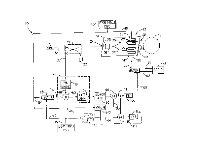
Fig. 1 illustrates a schematlc block diagram of a
hybrld fiber/lntegrated optlc flber optlc gyro contalnlng the
apparatus of the present lnventlon;
6415~-1225
2083~4
NO 91/19166 PC~r/US91/03678
Fig. 2 illustrates a graph of light intensity
versus rotation rate phase difference as may be
measured in the fiber optic gyro of Fig. 1;
Fig. 3 illustrates the graph of Fig. 2 with a
5 square wave modulation signal and the resulting output
of the fiber optic gyro of Fig. 1 with no gyro
rotation;
Fig. 4 illustrates the graph of Fig. 2 with a
square wave modulation signal and the resulting output
of the fiber optic gyro of Fig. 1 with the gyro
undergoing rotation; and
Fig. 5 illustrates signal waveforms as measured at
various locations in the fiber optic gyro of Fig. 1.
Best Mode for Carrying Out the Invention
Illustrated in Fig. 1 is a modern interferometric
fiber optic rotation sensor, specifically a fiber optic
gyro (FOG) 10 of the hybrid fiber/integrated optic (IO)
type. The FOG has a number of system components
fabricated directly onto an IO device 12, with the
remainder of the system components external thereto.
As compared to prior art all-fiber FOG designs, the IO
device 12 improves FOG system closed-loop performance.
The FOG 10 includes a low coherence light source
14, e.g., a galium arsenide (GaAs) laser, which outputs
a beam of low coherence light at a wavelength of, e.g.,
0.8 microns, into a single mode optical fiber 16. The
light propagates through the fiber 16 to a fiber optic
directional coupler 18. The coupler 18 may have a
coupling coefficient off e.g., 50%; thus, half of the
light input to the coup~er from the source 1~ is
coupled by evanescent fi~-ld coupling into a second
fiber 20 and is terminated non-reflectlvely by a light-
absorbing terminator 22. A suitable fiber optic directional
coupler is described in U.S. Patent No. 4,735,506 to Pavlath.
The portion of the light not lost from the coupler
18 propagates through the fiber 16 to a port 24 of the IO
device 12. If desired, the coupler may attach directly to the
IO device, thus eliminating any fuslon splices and reducing
component connections and associated alignments. Means and
me~hod for mounting optical fibers to an IO device are
disclosed in commonly owned U.S. Patent No. 4,871,226 to
Courtney et al.
The IO device may be comprised of, e.g., lithium
n~obate, LiNbO3, or lithium tantalate, with waveguides
26,28,30 being formed therein by known titanium indiffusion or
proton exchange techniques. As illustrated in Fig. 1, the
endfaces 32,34 of the IO device are angled at approximately,
e.g., ten (lOJ degrees to reduce interface reflections between
the IO device and the fibers.
After entering the IO device 12, the light propa-
gates along the waveguide 26 where it undergoes polarizationby a polarizing filter 36. The polarlzer 36 transforms the
arbitrary polarization state of the light into a desired
polarization state, whlch is requlred to lnsure reciproclty ln
FOG performance. As described hereinafter, the light also
passes through the polarizer after propagating through the
fiber coil. Passing the light through the polarizer in both
directions of travel eliminates the birefringence phase
B 64159-1225
2083~6~ ~
lO 91tl9166 P(~r/US91/03678
difference caused by the different velocities of
propagation in the two possible polarization modes.
Upon leaving the polarizer, the light propagates
along the waveguide 26 until split into two equal
beams. Each beam propagates along the corresponding
waveguide 28,30 until it exits the IO device at an
appropriate port 38,40. Coupled to each port 38,40 is
an end of a coil 42 of fiber optic cable, through which
the light beams counterpropagate before reentering the
IO device 12. The coil 42 comprises the rotation rate
sensing loop of the FOG 10.
In accordance with the well-known Sagnac effect,
any rotation of the coil about an axis perpendicular to
the plane of the coil causes the counterpropagating
light beams to travel unequal distances with respect to
one another. Rotation rate is determined by
recombi~ing the beams interferometrically and sensing
the amount of phase difference therebetween with a
photodetector. The light intensity varies since, due
to rotation, the light beams are at different phases
with respect to one another.
The diameter of the coil and length of the fiber
are application-specific. To gain sensitivity, a large
coil diameter, e.g., three inches, is desired. On the
other hand, the fiber length is a tradeoff between
cost, sensitivity and electronic signal processing
considerations. As fiber length decreases, the optimal
eigenfrequency increases, which increases the
complexity of the demodulator circuit. In general,
fiber lengths in the 100 to 300 meter range are common.
After propagating through the coil 42, each light
beam reenters the IO device and propagates in the
corresponding waveguide 28,30 in a reverse direction
2 0 8 ~
WO91/191~ ~ PCT/US91/0-
from which it originally came from the source 14. The
beams then recombine into one beam, pass through the
polarizer 36, and exit the IO de~ice at the port 24.
The beam then propagates along the fiber 16 to the
coupler 18, which couples, e.g., 50% of the beam along
the second fiber 20 to a detector 44.
The detector 44 may typically comprise a known PIN
photodiode or avalanche photodiode (APD). APDs offer
high sensitivity and better signal to noise ratios for
small signals. However, APDs require more complex
support circuitry, including a stable high voltage
supply. On the other hand, PIN diodes require simple
support circuitry and low voltage, and have relatively
good temperature stability and a lower cost.
In Fig. 1, the detector 44 comprises in part a PIN
diode 46. The PIN diode senses light impinging thereon
and converts the light into an electrical signal. The
electrical signal is provided on a line 48 to a summing
junction 50, which typically comprises the inverting
input of an operational amplifier (op-amp). The
summing junction output is fed to a detector
transimpedance amplifier 52, which comprises the
aforementioned op-amp connected in the known inverting
amplifier configuration (not shown), i.e., with a
resistor connected between the output and inverting
input and with the non-inverting input connected to
ground.
In a typical FOG processing sche~e for the
rotation rate signal, it is known to use both open and
closed loop configurations. In an open loop FOG, the
rotation rate signal is determined from the intensity
of the recombined light beam signal. The closed loop
approach uses the rotation rate signal to induce a
20839~ ~
/091/19166 PCT/US91/03678
~............................ 9
phase bias into the light beams counterpropagating in
the fiber coil. This phase bias is equal to the
negative of the rotation-induced Sagnac phase shift,
which nulls out the Sagnac phase shift. Thus, the
induced phase shift is a measure of the rotation rate.
As compared to an open loop system, a closed loop
system has reduced sensitivity to environmental errors,
linear scale factor, and extended dynamic range. The
present invention may be implemented in either an
open-loop or closed-loop FOG. A closed-loop FOG is
illustrated in Fig. l.
To achieve the desired nulling phase shift of the
light beams, a phase modulator 54 is fabricated on the
IO device along on'e waveguide 30. The phase modulator
54 may be driven by a repetitively linear ramped or
staircased electrical signal. If the peak ramp or
staircase amplitude is 2 * PI radians, and the flyback
following each ramp segment is essentially
instantaneous, the resulting serrodyne modulation
acting on the counterpropagating light beams at
different times produces an effectively constant phase
difference between the two beams. The magnitude of the
phase bias is proportional to the ramp slope (and thus
its frequency), which constitutes an easily and
accurately measurable representation of FOG rotation
rate.
The serrodyne modulator 54 is fabricated on the IO
device 12 by depositing metal electrodes 56, utilizing
a known photolithographic process similar to that used
in the microelectronics industry. The signal driving
the serrodyne modulator is typically bipolar in nature
and is supplied on a line 58 from known ramp generation
circuitry 60. The ramp circuitry also includes counter
2083!~6 1
WO91/19166 PCT/US91/0
circuitry which determines the polarity of the bipolar
signal and provides a pair of signals on lines 61,62 to
a suitable display device 66 for display of rotation
rate. A first signal on the line 61 is indicative of
positive rotation rate while a second signal on the
line 62 is indicative of negative rotation rate.
When the FOG l0 is at rest (i.e., no rotation),
the counterpropagating beams in the coil 42 travel
equal path lengths and are of equal phase at the
detector 44, resulting in maximum light intensity.
Fig. 2 illustrates a graph 70 of the cosine
relationship between the intensity (I) of the optical
signal (i.e., the recombined light beam) at the
detector and the Sagnac rotational phase difference (S)
between the counterpropagating light beams. The Sagnac
phase difference in radians is given by:
S = ((2 * PI * L * D)/ WL * C) * RR (equ.
1)
where:
L is the fiber coil length in meters; D is the
diameter of the fiber coil in meters; WL is the
wavelength of light in the coil in meters; C is the
speed of light in meters per second; RR is the rotation
rate in radians per second.
The intensity, I, of the light beam impinging on
the detector is a function of the Sagnac phase
difference between the light beams, as given by:
I = Il + I2 + 2(Il * I2)l/2 * COS(S) (equ-
2)
where:
208396 4 ~
~91/19166 PCT/US91/03678
11
I1 and I2 are the intensities of the individual
light beams counterpropagating in the coil.
Fig. 2 is a graph 70 of equation 2. Thus, the
intensity of the light beam at the detector is maximum
when the Sagnac phase difference is zero. However, due
to the cosine nature of the curve, the signal intensity
is relatively insensitive to small changes in phase
difference between the counterpropagating beams, these
small phase changes being caused by correspondingly
small rotation rates. Such insensitivity makes it
difficult to transform the intensity at the detector
into an accurate signal indicative of rotation rate.
Referring to Fig. 3, it is known to induce an
additional dither phase bias onto the
counterpropagating beams to maximize FOG sensitivity at
low rotation rates. The dither phase bias may be a
square wave modulation imposed on one end of the fiber
coil, as illustrated by the waveform 72. However, it
is to be understood that a sinusoidal modulation may be
used, if desired. Fig. 3 illustrates the FOG with zero
rotation, resulting in a DC level output waveform 74.
Referring to Fig. 4, during rotation, the square
wave bias 72 is asymmetric about the cosine
characteristic and the output waveform 74 contains a
component of the modulation frequency. The amplitude
of the output waveform is related to the phase shift in
a sinusoidal fashion (as opposed to cosinusoidally).
This results in increased and approximately linear FOG
sensitivity at low rotation rates. Also, by making the
modulation frequency equal to one-half times the
reciprocal of the optical transit time through the loop
(i.e., the eigenfrequency), the effectiveness of the
- 208:~9~ ~
WO91/191~ PCT/US91/0~3
12
dynamic bias modulation is optimized, the effects of
certain error sources (such as inadvertent amplitude
modulation and duty cycle asymmetry) are minimized, and
overall FOG performance is improved. Known synchronous
; demodulation techniques may be used with this square
wave dither modulation.
Referring to Fig. l, the dither phase bias is
induced by placing an optical phase modulator 80 along
the waveguide 28. The dither modulator 80 is
fabricated on the IO device 12 using a pair of
electrodes 82 in a similar fashion to the serrodyne
modulator 54 described hereinbefore. The dither
modulator is driven by a signal on a line 84 from a
square wave oscillator 86 at the eigenfrequency.
In accordance with the present invention, the
output of the eigenfrequency oscillator on the line 84
is fed to a +/- 90 degree (quadrature) phase shifter
88, which shifts the phase of the eigenfrequency signal
plus or minus ninety (90) degrees. This phase shifting
is in response to a square wave modulation signal on a
line 90 from a low frequency oscillator 92. The
modulation signal has a peak to peak amplitude of 180
degrees at a relatively low frequency of, e.g., l0 KHz,
the l0 KHz frequency being higher than the bandwidth of
2s the sensor's signal processing electronics. A
quadrature signal on a line 94 from the quadrature
phase shifter'88 is fed to the summing junction 50.
The detector transimre~nce amplifier 52 provides an
amplified signal to a demodulator amplifier 96.
The output of the demodulator amplifier 96 is fed
to a first mixer 98 (i.e., demodulator), the other
input of which is provided on a line l00 from a
variable phase shifter 102. The input to the variable
20839~
.JO91/19166 13 PCT/US91/03678
phase shifter 102 is the output of the eigenfrequency
oscillator 86 on the line 84.
The output of the first mixer 98 is provided on a
line 104 to a first integrator 10~, which integrates
the resulting rotation rate signal out of the first
mixer and provides an integrated rate signal on a line
108 to the ramp circuitry 60. The output of the first
mixer is also provided on the line 104 to a second
mixer 110 (demodulator), the other input of which is
the output of the low frequency oscillator 92 on the
line 9o. The output of the second mixer 110 is fed to
a second integrator 112, which integrates the second
mixer output signal and provides an integrated output
signal on a line 114. As described hereinafter, this
integrator output signal adjusts the phase of the
output of the variable phase shifter 102 according to
the amount of unwanted phase shift of the rotation rate--
signal.
In operation, the present invention measures the
unwanted phase shift to the sensed rate signal caused
by both the detector transimpedance amplifier 52 and
demodulator amplifier 96 and compensates for it while
applying the rate signal to the ramp circuitry. First,
the modulated square wave signal on the line 94 is
added in quadrature to the measured rate signal on the
line 48. Then, the detector transimpedance amplifier
and demodulator amplifier undesirably shift the phase
of both the square wave signal and rate signal by an
equal amount.
Passing through the first mixer 98 is the low
frequency component of the shifted modulated square
wave signal, the amplitude of which is ideally zero
when the loop is closed, and the undesirably phase
2 0 8 3 ~
WO91/191~ PCT/US91/03
14
shifted quadrature signal is in quadrature with the
variably phase shifted reference signal. The amplitude
of the low frequency component of this signal is
demodulated at the second mixer 110 with the reference
square wave modulation signal from the low frequency
oscillator 92. The resultant magnitude and sign
necessarily represents the amount and sense of
undesired phase shift to the rate signal. This
difference is integrated by the second integrator 112
lo and applied to the variable phase shifter, which shifts
the phase of the eigenfrequency signal on the line 84
to exactly match the phase of the rate signal as
applied to the first mixer. The undesired phase shift
in the rate signal is thus cancelled out at the first
mixer, and the resulting optimally demodulated rate
information is fed to the first integrator.
Illustrated in Fig. 5, illustrations (a)-(j), are
binary (positive, negative) logic state electrical
signal waveforms measured at various points in the FOG
of Fig. 1. Fig. 5(a) illustrates a waveform 120 of the
eigenfrequency signal on the line 84 from the
eigenfrequency oscillator 86. Fig. 5(b) illustrates a
waveform 122 of the square wave modulation signal on
the line 90 from the low frequency oscillator 92. This
- 25 signal is at a frequency of, e.g., 1/100 times that of
the eigenfrequency.
Fig. 5(c) illustrates a waveform 124 of the
eigenfrequency signal on the line 94 at the output of
the quadrature phase shifter 88. This signal
alternately shifts its phase to either lead or lag the
waveform 120 of the eigenfrequency signal by ninety
degrees depending on the logic state of the square wave
modulation signal waveform 122. Fig. 5(d) illustrates
208396~
O 91/19166 15 PCr/US91/03678
a waveform 126 of the sensed rotation rate signal on
the line 48 from the PIN diode 46. In ideal operation
of the present invention, the rotation signal waveform
126 is in phase with the eigenfrequency signal waveform
5 120. Although not shown, the rotation signal includes
a component in quadrature with the eigenfrequency
signal, this component being representative of an
inherent error sensed by the rotating fiber coil.
Fig. 5(e) illustrates a waveform 128 of the
10 rotation signal (~ig. 5(d) ? after the inherent
undesirable phase shift caused by the detector
transimpedance amplifier and the demodulator amplifier
(times T1-T2). In this exemplary embodiment, the phase
shift is 45 degrees. However, it is to be understood
15 that the amount of undesirable phase shift depends upon
the component characteristics of the aforementioned
amplifiers. Fig. 5(f) illustrates a waveform 130 of
the eigenfrequency signal at the quadrature phase
shifter output (Fig. 5(c)) after the phase shift of 45
20 degrees by the amplifiers (times T4-T5).
Fig. 5(g) illustrates a waveform 132 of the
variable phase shifter output signal. As described
hereinbefore, the first and second mixers 98,110 and
the second integrator 112 control the phase of the
25 variable phase shifter output 132 to equal the phase of
the undesirably phase shifted rotation signal (Fig.
5(e)). Fig. 'S(h) illustrates a waveform 134 of the
undesirably phase shifted rotation signal after being
mixed with the variable phase shifter output. Although
30 not shown, the DC level of the signal of Fig. 5(h) is
at its maximum value since this signal is at a constant
positive logic level. That is, if the signal of Fig.
5(h) had excursions to the binary negative logic state,
2o~3~6~
WO91/191~ 16 PCT/US91/0-
the DC level of that signal would be less than its
maximum value. These negative excursions occur if the
phase of the variable phase shifter output is unequal
to the phase of the undesirably phase shifted rotation
signal. Thus, the signal of Fig. 5(h) represents the
ideal control state attained by the present invention,
this signal being subsequently integrated by the first
integrator 106 and fed to the ramp circuitry 60.
Fig. 5(i) illustrates a waveform 136 of the
undesirably shifted quadrature phase shift signal after
being mixed with the variable phase shifter output
signal. Fig. 5(j) illustrates a waveform of Fig. 5(i)
after being mixed in the second mixer llO with the
square wave modulation signal 122 (Fig. 5(b). The
signal of Fig. 5(j) is fed to the second integrator 112
and the integrated signal is provided to the variable
phase shifter 102. Although not shown, the DC level of
Fig. 5(j) is nearly zero in the exemplary embodiment of
Fig. 5, indicating that the present invention has
reached the desired control state of zero phase
difference between the rotation rate signal and the
serrodyne modulator excitation signal.
If the phase of the undesirably shifted quadrature
phase shift signal is not in quadrature with the phase
of the output of the variable phase shifter (i.e., the
2s two inputs to the first mixer), then the output of the
second mixer'would not have such a 50% duty cycle as
illustrated in Fig. 5(j). Instead, the output signal
of the second mixer would have a more asymmetrical duty
cycle, the amount of asymmetry depending on the
magnitude of the phase difference between the two input
signals at the first mixer. It follows that the DC
level of the asymmetric signal of Fig. 5(j) would not
2083964 :-
~091/19166 PCT/US91/03678
17
be zero, but instead would be either a positive ornegative value the magnitude of which is proportional
to the asymmetry. This DC level is then integrated and
applied to the variable phase shifter such that the
amount of the output of the second integrator causes
the variable phase shifter to shift its phase
accordingly so as to match the phase of the undesirably
phase shifted rotation rate signal. The result is then
the 50% duty cycle signal of Fig. 5(j).
Illustrated in phantom in Fig. l is an optional
open loop phase shifter lS0 fed by the signal from the
low frequency oscillator on the line 9o. The shifter
150 adds a few degrees of phase shift to the signal on
the line 90 before applying it to the second mixer llO.
The added phase shift makes the phase difference
between the shifted rate signal (Fig. 5(e)) and the
rate signal (Fig. 5(d)) essentially zero by
compensating for the residual phase error between the
shifted rate signal at the first mixer 98 and the
signal on the line lO0 from the variable phase shifter
102. This residual phase error is approximately equal
to the phase shift between the shifted rate signal
(Fig. 5(e)) and the rate signal (Fig. S(d)), divided by
the frequency ratio of the eigenfrequency signal (Fig.
5(a)) to the low frequency oscillator signal (Fig.
5(b)). Thus, the lower the frequency of the low
frequency oscillator signal, then the lower the amount
of the residual phase shift.
The present invention has utility in compensating
for undesirable and inherent variable phase shifts in
the measured rotation rate signal in a fiber optic
rotation sensor, the variable shifts due in part to
~ thermal and aging factors. The result is a more
2083~6'1
WO91/191~ 18 PCT/US91/0~ 3
accurate measure of rotation rate. Also, the present
invention does not undesirably change the magnitude of
the sensed rate signal since the shifted eigenfrequency
signal is added in quadrature to the sensed rate signal
and also since the frequency of the low frequency
carrier is beyond the bandwidth of the sensor's signal
processing electronics.
The present invention is illustrated for use in a
closed-loop FOG. However, the present invention may be
used, if desired, in an open-loop FOG, or other types
of fiber optic rotation sensors in a manner which
should be apparent from the teachings herein. Also,
the invention is illustrated as variably shifting the
phase of a signal at the coil eigenfrequency for
subsequent demodulation of rotation rate information
which itself is modulated at or near the
eigenfrequency. Typically, the modulator is set at the
coil eigenfrequency for FOG performance reasons. To
fully demodulate the rotation rate information, the
demodulator reference signal (i.e., the output from the
variable phase shifter) is also at the eigenfrequency.
It suffice, however, for the present invention that the
modulation and demodulation frequencies be equal.
It suffice for the broadest scope of the present
2j invention that a fiber optic rotation sensor having a
pair of light beams counterpropagating in a loop
includes a phase modulator for modulating the waves at
a first frequency, upon exiting the loop the waves are
combined into a light intensity signal indicative of
rotation rate and is sensed, a signal at the first
frequency is quadrature phase shifted by a lower
frequency signal and summed with the sensed rate
signal, an amplifier amplifies the summed signals, the
2083964
~O91/19166 PCT/US91/03678
19
amplifier also inherently induces undesirable phase
shifts by an equal amount in both the sensed rate
signal and the quadrature signal, the quadrature signal
is demodulated and used in feedback fashion to control
the phase of a variable phase shifter which provides a
signal at the first frequency whose phase is shifted by
an amount equal to the undesirable phase shift of the
sensed rate signal, the variable phase shifter signal
and the sensed rate signal being provided to a
demodulator to demodulate rotation rate information
from the sensed rate signal.
Although this invention has been shown and
described with respect to detailed embodiments thereof,
it will be understood by those skilled in the art that
various changes in form and detail thereof may be made
without departing from the spirit and scope of the
claimed invention.
We claim: