Note : Les descriptions sont présentées dans la langue officielle dans laquelle elles ont été soumises.
2~3~
SPECIFICATION
Title of the Invention
CONNECTION OF SUPERCONDUCTING CURl~ENT
S PATHS FORMED OF OXIDE SUPERCONDUCTOR
MATERIAL
Background of the Invention
Field of the invention
The present inventioll relates to a connection of superconducting
current paths formed of an oxide superconductor material. More
specifically ~o ~ connection of superconducting current paths formed of an
o~ide superconductor material, through which superconducting current
flows efficiently.
Description of related art
A superconducting current path is one of the electronic applications
of a superconductor. If all the curlellt path~ of a conventional electronic
- circuit including semiconductor devices is replaced with superconducting
current paths, completely, the electronic circllit will operate rapidly with
low power consumption. Superconducting signal paths are also expected
to reduce the wave form distortion so that the required number of
amplifiers and/or repeaters can be reduced. Particularly, by using an
oxide superconductor material which has been recently advanced in study,
2~ it is possible to produce a superconducting current path through which
superconducting current flows at relatively high temperature.
- 1 -
2 ~ B .Fi4 ~
In order to apply the superconduc~ing current path of an oxide
superconductor to a superconducting circuit, the superconducting current
path is connected to another one or an device. It should also be taken into
consideration a superconducting multilayer interconnection utilizing the
S oxide superconductor.
An oxide superconductor has the largest critical current density Jc
in direction perpendicular to c-axes of its crystal lattices. Therefore, it is
desirable that the superconducting current path through which
superconducting current flows horizontally is formed of a c-axis
10 orientated oxide superconductor thin ~ïhn cmd the superconducting path
through which superconductillg current flows vertically is folmed of
oxide superconductor thin films of which the c-axis is orientated
horizontally. ~n this specification, this oxide superconductor thin film of
which the c-axis is orientated llorizontally will be called an "a-axis
15 orientated oxide superconductor thin film".
A Josephson junction device is one of superconducting devices
- which is constituted of two superconducting electrodes joined by a
Josephson junction. The Josephson 3unction can be realized in various
structures. Among the various structures, the most preferable structure
20 in practice is a stacked junction realized by a tliin non-superconductor
layer sandwiched between a pair of superconductors. However, a point
contact type junction and a Dayem bridge type junction which are
composed of a pair of superconductor regions which are weakly linked to
each other also exhibit Josephson effect. In general, these Josephson
2 5 junctions have fine structures in which the superconductor and/or
non-superconductor are composed of thin films.
- 2~8~
In order to realize a stacked type junction by using an oxide
superconductor, a first oxide superconductor thin film, a non-
superconductor thin film and a second oxide superconductor thin film are
stacked on a substrate in the named order.
S In the above men~ioned stacked type junction, an insulator MgO
etc., a semiconductor Si etc., and a metal Au etc. are used for ~he non-
superconductor layers so that each superconducting junction has different
properties for each application.
The thickness of the non-superconduc~or layer of the stacked type
10 junction is deterrnined by the coherence length of the superconductor. ~n
general, the thickness of the non-superconductor layer of the stacked type
junction must be within a few times of the coherence length of the
superconductor. On the other lland, since oxide superconductor materials
have a very short coherence length, therefore, a thickness of a non-
1 5 superconductor layer must be about a few nanometers.
However, the superconductor layers and the non-superconductor
layer of the staclced type junction must be of high crystallinity for
favorable junction properties, which are composed of single crystals or
composed of polycrysta~s which are orientated in almost same direction.
2 0 It is difficult to stac3i an extremely thin and high crystalline
non-superconductor layer on all oxide superconductor layer.
Additionally, it is very difficu It to st~ck a high crystalline oxide
superconductor layer on the non-superconductor layer stacked on the first
oxide superconductor layer. Thougll the stacked structure including a
2 5 first oxide superconductor layer, a non-superconductor layer and a second
oxide superconductor layer is realized, the illterfaces between the oxide
superconductor layers and the non-superconductor layer are not in good
2 ~
condition so that the stacked type jUIICtiOll does not function in good
order.
In order to manufacture a point contact type junc~ion and a Dayem
bridge type junction by using oxide superconductor, very fine processings
S which re~lize a weak link between a pair of superconductor are necessary.
It is very difflcult to conduct a fine processing with good repeatability.
The point contact type jUIlCtiOIl has been formed of two oxide
superconductor thin films which are in contact with each other in a
-extremely small area which cons~itutes the weak lin~ of the Josephson
1 0 junction.
The Dayem bridge type junction has been iormed of a constant
thickness oxide superconductor thill film which is formed on a su~strate
and which is patterned in a plan view, so that a superconductor thin film
region having a greatly narrow width is formed between a pair of
15 superconductor thin film regions having a sufficient width. In other
words, the pair of superconductor thin film regions having a sufficient
width are coupled to each other by the superconductor thin film region
having the greatly narrow width. Namely, a weak link of the Josephson
junction in the superconductor thin film is formed at the greatly narrow
2 0 width region.
In order to resolve the above mentio1led problems, so-called
variable thickness bridge type ~osephson device is proposed in a prior art.
The variable thickness bridge type junction has been formed of an oxide
superconductor thin film of a sufficient thicklless which is formed on a
2 S substrate having a projection and which is p~rtially thinned in a thickness
direction on the projection of the substrate, so ~hat a thinned oxide
superconductor thin film portion is formed between a pair of
superconductor thin films having the sufficient thickness. In other words,
the pair of superconductor thin film portions having the sufficient
thickness are coupled to each other by the thinned oxide superconductor
thin film portion. Accordingly, a weak link of the Josephson junction is
S fo~ned at the reduced thickness portion of tlle oxide superconductor thin
film.
No fine processing, which is required to manufacture a point
contact type Josephson junction device or a Dayem bridge type Josephson
junction device, is necessary to manufacture the above mentioned variable
10 thickness bridge type Josephson junctioll device
Josephson device is one o~ well-known superconducting devices.
However, since Josephson device is a two-terminal device, a logic gate
which utilizes Josephson devices becomes complicated. Therefore,
three-teImina1 superconducting devices are more practical.
Typical three-terminal superconducting devices include two types of
super-FFT (field effect transistor). The first type of the super-FET
includes a semiconductor channel, and a superconductor source electrode
and a superconductor drain electrode which are formed closely to each
other on both side of the semiconductor channel. A portion of the
2 0 semiconductor layer ~etween the superconductor source electrode and the
superconductor drain electrode has a greatly recessed or undercut rear
surface so as to have a reduced thickness. In addition, a gate electrode is
~ormed through a gate insulator layer on the portion of the recessed or
undercut rear surface of the semiconductor layer between the
2 5 superconductor source electrode and the superconductor drain electrode.
A superconducting currellt flows through the semiconductor layer
(channel) bet~Neen the superconductor source electrode and the
~'.;55~
superconductor drain electrode due to a superconducting proximity effect,
and is controlled by an applied gate voltage. This type of the super-FET
operates at a higher speed wit.h a low power consumption.
7'he second type o~ the super-FET includes a channel of a
S superconductor formed between a source electrode and a drain electrode,
so that a current flowing through the superconducting channel is
controlled by a voltage applied to a gate formed above the
superconducting channel.
Both of the super-FETs mentioned above are voltage controlled
devices which are capable of isola~ing output signal from input one and of
h~ving a well defined gain.
However, since the first type of the super-FET utilizes the
superconducting proximity effect, the superconductor source electrode
and the superconductor drain electrode have to be positioned within a
l S distance of a few times the coherence length of the superconductor
materials of the superconductor source electrode and the superconductor
drain electrode. In particular, since an oxide superconductor has a short
coherence length, a distance between the superconductor source electrode
and the superconductor drain electrode has to be made less than about a
few ten nanometers, if the superconductor source electrode and the
superconductor drain electrode are ~ormed of the oxide superconductor
material. However, it is very difficult to conduct a fine processing such
as a fine pattern etching, so as to satisfy the very short separation distance
mentioned above~
On the other hand, the supel-FET having the superconducting
channel has a large current capability, and the fine processing which is
2 ~
re~uired to product the first type of the super-FET is not needed to
product ~is type of super-FET.
In order to obtain a complete ON/OFF operation, both of the
superconducting channel and the gate insulating layer should have an
5 extremely thin thickness. For example, the superconducting channel
formed of an oxide superconductor material should have a thickness of
less than five nanometers and the gate insulating layer should have a
~ickness more than ten nanometers which is sufficient to prevent a tunnel
current.
In a prior art, a superconducting multilayer interconnection which
has layered superconducting current paths constituled of c-axis orientated
oxide superconductor thin films and a superconducting interconnect
current path constituted of an a-axis orientated oxide superconductor ~in
film is proposed. However, grain boundaries are genera~ed at the
15 interface between the c-axis orientated oxide superconductor thin ~llm and
the a-axis orientated oxide superconductor thin film, which introduce
difficulties of supercol-ducting current flow. The grain bo~ndaries
sometimes form Josephson junctions whicll pass only tunnel current so
- that the current capability is lilnited and the input and output relationships20 become nonlinear. Even if no Josephson junction is formed at the
interfaGe, Joule heat may be generated by the electrical resistance formed
at the interface, which causes the "quench" phenomenon. Furthermore,
the c-axis orientated oxide superconductor thin film and the a-axis
orientated oxide superconductol thin film may interfere with each other
2 5 so as ~o degrade them both.
The above variable thickness bridge type Josephson device and
superconducting field effect device have portions at which thickness of ~e
2Q84551
oxide superconductor thin films decreases sharply. The directions of
superconducting current flow suddenly change at these portions so that the
superconducting current capability is limited by these portions of the
oxide superconductor thin films.
In this case, the superconducting current does not always flow in the
direction pel~..dicular to the c-axes of the oxide supercon~ ctQr crystals,
so dlat the supercon~ cting cu~lell~ can not flow efficiently.
Summary of the Invention
An object of the present invention is to provide a superconducting
10 device such as a Josephson junction device or an FET type device which
addresses the above mentioned defects of the prior art.
According to the present invention there is provided a
superconducting device comprising a substrate having a principal surface, an
insulating region projected on the principal surface of the substrate and an
15 oxide superconductor thin film formed on the principal surface of the
substrate, which has a planar surface, two thick portions at the both sides of
the insulating region and one thin portion on the insulating region wherein
:B
2n8~55~
the insulating region has a trapezoid shape cross section of which both
opposite side surfaces are inclined at an angle of less than 40~ to the principal
surface of the substrate in which the thick portions of the oxide
superconductor thin film and the thin portion of the oxide superconductor
5 thin film are smoothly connected to each other along the inclined side
surfaces of the insulating region so as to avoid abrupt change of sectional area
of the oxide superconductor thin film so that current can efficiently flow
between the thick portions and the thin portion.
In a preferred embodiment, the oxide superconductor is formed of
10 high-TC (high critical temperature) oxide superconductor, particularly, formed
of a high-TC copper-oxide type compound oxide superconductor for example a
Y-Ba-Cu-O compound oxide superconductor material and a Bi-Sr-Ca-Cu-O
compound oxide superconductor material.
In addition, the substrate can be formed of an insulating substrate,
preferably an oxide single crystalline substrate such as MgO, SrTiO3,
CdNdAl04, etc. These substrate materials are very effective in forming or
growing a crystalline film having a high degree of crystalline orientation.
A superconducting circuit may comprise a substrate, a superconducting
current path of an oxide superconductor thin film formed on the substrate
20 through which superconducting current flows at a direction parallel to the
substrate and an electronic device connected to the superconducting current
5 5 11
path in which the interface between the superconducting current path and the
electronic device is inclined at an angle less than 40~ to the substrate so thatthe superconducting current path is smoothly connected to the electronic
device.
A superconducting multilayer interconnection may comprise a
substrate having a principal surface, a first superconducting current path of a
c-axis orientated oxide superconductor thin film formed on the principal
surface of the substrate, an insulating layer on the first superconducting
current path and a second superconducting current path of a c-axis orientated
oxide superconductor thin film formed on the insulating layer so that the first
and second superconducting current paths are insulated by the insulating
layer, in which the second superconducting current path has a portion which
penetrates through the insulating layer and contact with the first
superconducting current path and the portion is inclined at an angle less than
40~ to the substrate so that the first and second superconducting current paths
are smoothly connected to each other.
The above and other objects, features and advantages of the present
invention will be apparent from the following description of preferred
embodiments of the invention with reference to the accompanying drawings.
- 10 -
~ Q ~1 ~ 5 ~ ~
Brief Description of the Drawings
Figure 1 is a diagrammatic enlarged sectional view of a characteristic
part of an embodiment of the superconducting circuit;
Figure 2 is a diagrammatic sectional view of a first embodiment of the
5 superconducting multilayer interconnection;
Figure 3 is a diagrammatic sectional view of a second embodiment of
the superconducting multilayer interconnection;
Figure 4 is a diagrammatic sectional view of an embodiment of the
Josephson junction device in accordance with the present invention; and
10Figure 5 is a diagrammatic sectional view of an embodiment of the
super-FET in accordance with the present invention.
Embodiment 1
Referring to Figure 1 an embodiment of a superconducting circuit will
15be described. Figure 1 shows a diagrammatic sectional view of a characteristic
part of an embodiment of the superconducting circuit.
The superconducting circuit includes a resistor 40 of Y1Ba2Cu3O7 ~
oxide semiconductor arranged on a principal surface of an MgO (100) substrate
5 and superconducting current paths 11 and 12 of YlBa2Cu3O7 ~ oxide
20 superconductor, which are connected to the both ends of the resistor 40. Since
the superconducting current paths 11 and 12 are connected to the resistor 40 in
the same way, only the connection 30 of the superconducting current path 11
and the resistor 40 will be described.
- 11 -
~ ~ 8 ~ 5 5 ~ '
In the superconducting circuit, the superconducting current paths 11
and 12 ~-e formed of c a~ urlenhkd Y _
/
/
2~8~
superconductor thin films, since YlBa2Cu307 ~ oxide superconductor has
the largest cIitical current density in the direction perpendicular to c-axes
of its crystals. At the connection 30, the interface between the
superconducting current path 11 and the resistor 40 is inclined at an angle
a of 30~ to the principal surface of the substrate 5. Therefore, the
superconducting current path 11 does not deform sharply so that the
crystalline structure of the YIBa2Cu3O7 ~ oxide superconductor is not
disordered at ~e connection 30.
The superconducting circuit was manufactured by the following
1 0 process.
At first, the resistor 40 was formed of a Y1Ba2Cu3O7 ~ oxide
semiconductor thin film on the principal surface of the MgO (100)
substrate 5. The Y~Ba2Cu3O7 ~ oxide semiconductor thin film was
deposited by a sputtering and pattemed by a lift-off process utilizing CaO.
The condition of forming the YlBa2Cu3O7 ~ oxide semiconductor thin
film is as follows:
Temperature of the substrate 800 ~C
Sputtering Gas Ar: 90%
~2: 10%
Total pressure 5 x l0-2 Torr
Thickness of the thin film 300 nanometers
The both ends of the pattemed YlBa2C~307 ~ oxide semiconductor
thin film were processed by an ion beam etching so that the side surfaces
of the edges were Inclined at angle of 30~ to the principal surface of the
2 5 substrate 5. Then, the resistor 40 was completed. The resistor 40 had a
resistance of severa~ kQ.
~8~5
Thereafter, the superconducting current paths 11 and 12 were
formed of c-axis orientated YIBa2Cu3O7~ oxide superconductor thin films
on the principal surface of the substrate S. The c-axis orientated
YlBa2Cu3O7~ oxide superconductor thin films were formed by a
S sputtering. The condition of forming the c-axis orientated YlBa2Cu30
oxide superconductor ~in film by a sputtering is as follows:
Temperature of the substrate 700~C
Sputtering Gas Ar: 90%
~2: 10%
Total pressure S x lo-2 Torr
Thickness of the thin film 300 nanometers
A conventional superconducting circuit which had the same
structure as that of the above superconducting circuit was also formed
except a resistor didn't have processed edges. The resistance
1 5 measurements between the superconducting current paths 11 and 12 of the
two superconducting circuit were made under liquid nitrogen cooling. In
case of the superconducting circuit in accordance with the present
invention, the resistance value was the same as that of the resistor 40
itself. On the contrary, in case of the conventional superconducting
20 circuit, the value of the resistance was ten times larger than that of the
resistor. Therefore, in the superconducting circuit in accordance with the
present invention, the interface between the superconducting current path
and the resistor was improved.
2 S Embodiment 2
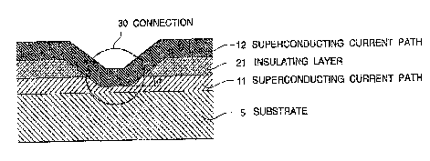
Referring to Figure 2 an embodiment of the superconducting
multilayer interconnection will-
- 14 -
' .~3
5 ~
be described. Figure 2 shows a diagrammatic sectional view of a
characteristic part of an embodiment of the superconducting multilayer
interconnection .
The superconducting multilayer interconnection includes a first
5 superconducting current path 11 formed of a c-axis orientated
YlBa2Cu307 ~ oxide superconductor ~in film on a principal surface of an
MgO substrate 5, an ins~ tin~ layer 21 formed of MgO or silicon nitride
on the superconducting current path 11 and a second superconducting
current path 12 formed of a c-axis orientated YlBa2Cu3O7 ~ oxide
10 superconductor thin film on the insulating layer 21. The substrate S may
includes a ground plane. The superconducting current path 12 has a
portion which constitutes an interconnect current path penetrating the
insul~ting layer 21 and contacting to the superconducting current path 11
at a connection 30.
The interconnect current path portion of the superconducting
current path 12 descends at an angle oc, penetrates the insulating layer 21,
smoothly contacts to the superconducting current path 11 and ascends at
an angle a. The angle oc should be less than 40~, otherwise the crystal
structure of the c-axis orientated YlBa2Cu307 ~ oxide superconductor thin
20 film which constitutes the superconducting current path 12 becomes
disordered at the interconnect current path portion.
Embodiment 3
Figure 3 shows another preferred embodiment of a
25 superconducting multilayer interconnection, which includes four layers of
superconducting current paths and two interconnect current path portions.
2~345~1
The superconducting multilayer interconnection includes an MgO
substrate 5, insulating layers 21 to 24 and superconducting current paths
11 to 14 which are stacked alternately on the s~bstrate 5. The insulating
layers 21 to 24 are formed of MgO or silicon nitride and the
S superconducting c~lrrent paths 11 to 14 are formed of c-axis orientated
YlBa2Cu307.~0xide superconductor thin films. The substrate 5 may
include a ground plane. The superconducting current path 13 has a
portion which constitutes an interconnect current path penetrating the
insulating layer 23 ~nd smoothly contacting to the supercondllcting
10 current path 12 at a connection 31 and the superconducting current path
14 has a portion which constitutes an interconnect current path
penetrating the insulating layer 24 and smoothly contacting to the
superconducting current path 13 at a connection 32. The tilt angles oc of
~e interconnect current path portions of the superconducting multilayer
15 interconnection are less then 40~ as is dle same as Embodiment 2. The
relation between distance Is between the connections 31 and 32 and the
widths lc is as follows:
ls ~ 2.5 x lc to 3.0 x lc
In the above superconducting multilayer interconnection, each of
Z 0 the interconnect current paths connects the two neighboring
superconducting current paths and does not connects three or more
superconducting current paths. Since an interconnect current path which
connects three or more superconducting current paths should require a
large horizonta] cross-sectional area because of current capability
2 5 requirement, the dens~ty of ~he wiring is decreased. In addition, a large
depression is ~ormed at an interconnect current path portion which
connects three or more superconducting current paths so that it becomes
- 16 -
2~8~
different to stack another superconducting currellt path on it. Therefore,
the ~nterconnect current path preferably connects only the two
neighboring superconducting current paths.
In the above superconducting multilayer interconnection, a
superconducting current path can be formed on a connection. Even a
superconducting current path which cross a interconnection current path
above it can be formed. Therefore, the superconducting multilayer
interconnection in accordance with the present invention has a high degree
of freedom of wiring superconducting current paths with interconnect
cu~rent paths so that a complicated wiring and a high density wiring can
be easily composed. Even if a complicated wiring is composed of the
superconducting multilayer interconnection, the current capability does
not decrease.
1 5 Embodiment 4
Referrillg to Figure 4 an embodiment of the Josephson iunction
device in accordance with the present invention will be desc~ibed.
Figure 4 shows a diagrammalic sectional view of an embodiment of the
Josephson junction device in accordallce with the present invention.
2 0 The Josephson junction device includes an MgO substra~e S having a
projecting insulating region 50 of which the cross section is a shape of a
trapezoid and superconducting electlodes 101 and 102 coupled to each
other by a weak link l0 of a Joseph~on junction on the insulating region
50. Each of the surfaces 51 of the insu~ating region 50 is inclined at angle
ocof35~.
The superconducting electrodes 101 and 102 and the weak link 10
are formed of a c-axis orientated YlBa2Cu307 ~ oxide superconductor thin
2~8~551
film, namely sufficiently thick portions of the c-axis orientated
YlBa2Cu~O7 ~ oxide superconductor thin film constitute the
superconducting electrodes 101 and 102 and a thin portion of the c-axis
orientated YlB~2Cu307 ~ oxide superconductor thin film between the two
thick portions constitutes the weak link 10. The c-axis orientated
YlBa2Cu307 ~ oxide superconductor thin film is constituted of uniform
crystalline YIBa2Cu307 ~oxide supercond~lctor even near the inclined
surfaces 51 of the insulating region 50. The uniformity of the c-axis
orient~ted YlBa2Cu3O7 ~ oxide superconductor thin film is achieved by the
inclined angles o~ of 35~ of the sur~aces 51 of the insu}ating region 50.
Since the Josephsoll junction device is forrned of an uniform c-axis
orientated YlBa2Cu3O7~0xide superconductor thin film and the the
superconducting electrodes 101 and 102 are smoothly connected to the
weak link portion 10, current flowing through the superconducting
electrodes 101 and 102 efficiently flows into or from the weak link
portion 10. Therefore, the ~osephson 3unction device has a high
performance.
The Josephson junction device was manuf~ctured by the following
process.
At first, an insulating region 50 having a height of 0.3 llm was
formed by an ion-milling using Ar gas on a principal surface of an
MgO (100) substrate 5 having a size of 15 mm x 8mm and a thickness of
0.5 mm. In order to incline the sur~aces 51 at angles a of 35~, the Ar
ions were ~rradiated diagonally. The inclined surfaces 51 can also be
2 5 formed by a side-etching using a seeking effect of-e~chunt.
Then, the substrate S was heated to a temperature of 350 to 400 ~C
under a pressure lower than l x l0-'~ Torr in order to clean the etched
- 18 -
surfaces. Thereafter, a c-axis orientated YIBa2Cu3O7 ~ oxide
superconductor thin film was formed on the principal surface of the
substrate S by a sputtering. The condition of forming the c-axis
oricnt~te~ YlBa2Cu307 ~ oxide superconductor thin ~llm by a sputtering is
S as follows:
Temperature of the substrate 700~C
Sputtering Gas Ar: 90%
~2: 10%
Total pressure 5 x 10⁻² Torr
Thickness of the thin film 3~0 nanometers
Finally, the c-axis orientated Y~Ba2C~3O7 ~ oxide superconductor
thin film was etched back so th~t a planar surface was fo~ned. Then, the
Josephson junction device in accordance with the present invention was
completed.
Embodiment 5
Referring to F~gure 5 an embodiment of the super-FET in
accordance with the present invention will be described. Figure 5 shows
a diagr~mm~tic sectional view of an embodiment of the super-FET in
2 0 accordance with the present invention.
The super-Fl~T includes an MgO subs~rate S having a projecting
insulating region 50 of which the cross section is a shape of a trapezoid
and a superconducting source region 2 and a superconducting drain
region 3 electrically connected by a superconducting channe~ 1 on the
25 insulating region 50. ~ach of the surfaces 51 of the insulating region 50
is inclined at angle a o~ 35~.
- 19 -
2~551
The superconducting source region 2 ~nd the superconducting drain
region 3 and the superconducting channel 1 are formed of a c-axis
orientated YlBa2Cu3O7 ~oxide superconductor thin film, namely
sufficiently thick portions of the c-axis orientated YIBa2Cu307 ~oxide
- 5 superconductor thin film constitute the superconducting source region 2
and the superconducting drain region 3 and a thin portion of the c-axis
orient~te~ YlBa2Cu307.~ oxide superconductor thin film between the thick
portions constitutes the superconducting channel 1. The superconducting
source region 2 and the superconductin~ drain region 3 have a thickness
of on the order of 200 nanometers and the superconducting channel has a
thickness of on the order of S nanometels. The gate insulating layer 7 is
forrned of silicon nitride or MgO having a thickness of on the order of 15
nanometers. The gate electrode 4 is formed of Au.
The c-axis orientated YIBa2Cu307 ~ oxide superconductor thin film
1 5 is constituted of unif~rm crystalline ~IBa2Cu3O7 ~ oxide supe~conductor
even near the inclined surfaces 51 of the insulating region 50. The
uniformity of the c-axis orientated YlBa2Cu3O7.~oxide superconductor
thin fi~m is achieved by the inclined angles oc of 35~ of the surfaces 51 of
the insulating region 50.
2 0 Since the superconducting portion of the super-FET is formed of an
uniforrn c-axis orientated YIBa2Cu3O7.~0xide superconductor thin film
and the superconducting channel ~ is smoothly connected to the
superconducting source region 2 and the superconducting drain region 3,
~ere is no undesired jUI7CtiOIl nor resistallce ~t this portion and current
2 5 flowing through the superconducting source region 2 and the
superconducting drain region 3 efficiently flows into or from the
- 20 -
2 Q~
superconducting channel 1. Therefore, the super-FET has a high
performance.
The super-FET was manufactured by the following process.
At first, an insulating region 50 having a trapezoid shape cross
section was fo~ned by a reactive ion etching or an ion-milling using Ar
gas on a principal surface of an MgO (100) substrate S. In order to
incline the surfaces 51 at angles a of 35~, ions were irradiated diagonally.
Then, the substrate 5 was heated to a temperature of 350 to 400 ~C
under a pressure lower than 1 x 10⁻⁹ Torr in order to clean the etched
surfaces. Thereafter, a c-axis orientated ~lBa2Cu3O7.~ oxide
superconductor thin ~ilm was formed on the principal surface of the
substrate 5 by a sputtering. The condition of forming the c-axis
orientated YlBa2Cu3O7 ~ oxide superconductor thin film by a sputtering is
as follows:
1 5 Temperature of the substra~e 700~C
Sputtering Gas Ar: 90%
~2 10%
Total pressure 5 x 10⁻² Torr
Thickness of the thin film 200 nanometers
2 0 Then, the c-axis orientated YlBa2Cu3O7.~ oxide superconductor thin
film was etched back so that a planar surface was formed. Thick portions
of the c-a~is orientated YIBa2Cu307 ~ oxide superconductor thin film at
the both sides of the insulating region 50 would be a superconducting
source region 2 and a superconducting drain region 3. A thin portion of
2 5 the c-axis orientated YIBa2Cu307 ~ oxide superconductor thin film on the
insulating region 50 would be a superconducting channel 1. A gate
ins~ ting layer 7 was formed of MgO or silicon nitride on a poltion of
- 2l -
2~8~
the c-axis orientated YlBa2Cu307 ~ oxide superconductor thin film above
the insul~ing region 50 and a gate electrode 4 was formed of Au on the
gate insulating layer 7. Metal electrodes might be formed on the
superconducting source region 2 and superconducting drain region 3, if
S necessary. Then, the super-FET in accordance with the present invention
was completed.
In the above mentioned embodiments, the oxide superconductor thin
fi~m can be formed of not only the Y-Ba-Cu-O compound oxlde
superconductor material, but also a high-Tc (high critical temperature)
10 oxide superconductor material, particularly a high Tc copper-oxide type
compound oxide superconductor material, for example a Bi-Sr-Ca-Cu-O
compound oxide superconductor material.
The invention has thus been shown and described with reference to
the spec;fic embodiments. However, it should be noted that the present
15 invention is in no way limited to the details of the illustrated structures
but converts and modifications may be made within the scope of the
appended claims.